

Advanced Reticle Inspection for Nanometer-Level Defect Detection
MAY 20, 20269 MIN READ
Generate Your Research Report Instantly with AI Agent
Patsnap Eureka helps you evaluate technical feasibility & market potential.
Reticle Inspection Technology Background and Nanometer Detection Goals
Reticle inspection technology emerged in the 1980s as semiconductor manufacturing began transitioning toward smaller feature sizes. Initially, optical inspection systems dominated the field, utilizing visible light microscopy to detect defects on photomasks used in lithography processes. These early systems could identify defects in the micrometer range, which was sufficient for the relatively large feature sizes of that era. As the semiconductor industry progressed through the 1990s, the demand for higher resolution inspection capabilities grew exponentially.
The evolution toward nanometer-level detection began with the introduction of deep ultraviolet (DUV) inspection systems in the late 1990s. These systems employed shorter wavelengths, typically 193nm and 248nm, enabling detection of defects smaller than 100 nanometers. The transition coincided with the industry's adoption of 0.25μm and 0.18μm process nodes, where traditional inspection methods proved inadequate for ensuring mask quality standards.
Advanced reticle inspection technology has undergone significant transformation with the integration of electron beam inspection systems. These systems, introduced in the early 2000s, provided unprecedented resolution capabilities, enabling detection of defects as small as 10-20 nanometers. The technology leveraged high-energy electron beams to scan mask surfaces with atomic-level precision, representing a paradigm shift from purely optical methods.
Current nanometer detection goals focus on achieving sub-10nm defect detection capabilities to support advanced process nodes including 7nm, 5nm, and emerging 3nm technologies. The primary objective involves developing inspection systems capable of identifying critical defects that could impact device yield, including line edge roughness variations, phase defects in extreme ultraviolet (EUV) masks, and contamination particles at the molecular level.
The technological roadmap emphasizes multi-modal inspection approaches combining optical, electron beam, and atomic force microscopy techniques. These hybrid systems aim to achieve comprehensive defect characterization while maintaining throughput requirements for high-volume manufacturing. Additionally, artificial intelligence integration has become crucial for distinguishing between actual defects and false positives, particularly as detection sensitivity increases to unprecedented levels.
Future detection goals include real-time inspection capabilities during mask fabrication processes, enabling immediate correction of manufacturing deviations. The industry targets achieving defect detection sensitivities below 5 nanometers while reducing inspection cycle times to support the economic viability of advanced node production.
The evolution toward nanometer-level detection began with the introduction of deep ultraviolet (DUV) inspection systems in the late 1990s. These systems employed shorter wavelengths, typically 193nm and 248nm, enabling detection of defects smaller than 100 nanometers. The transition coincided with the industry's adoption of 0.25μm and 0.18μm process nodes, where traditional inspection methods proved inadequate for ensuring mask quality standards.
Advanced reticle inspection technology has undergone significant transformation with the integration of electron beam inspection systems. These systems, introduced in the early 2000s, provided unprecedented resolution capabilities, enabling detection of defects as small as 10-20 nanometers. The technology leveraged high-energy electron beams to scan mask surfaces with atomic-level precision, representing a paradigm shift from purely optical methods.
Current nanometer detection goals focus on achieving sub-10nm defect detection capabilities to support advanced process nodes including 7nm, 5nm, and emerging 3nm technologies. The primary objective involves developing inspection systems capable of identifying critical defects that could impact device yield, including line edge roughness variations, phase defects in extreme ultraviolet (EUV) masks, and contamination particles at the molecular level.
The technological roadmap emphasizes multi-modal inspection approaches combining optical, electron beam, and atomic force microscopy techniques. These hybrid systems aim to achieve comprehensive defect characterization while maintaining throughput requirements for high-volume manufacturing. Additionally, artificial intelligence integration has become crucial for distinguishing between actual defects and false positives, particularly as detection sensitivity increases to unprecedented levels.
Future detection goals include real-time inspection capabilities during mask fabrication processes, enabling immediate correction of manufacturing deviations. The industry targets achieving defect detection sensitivities below 5 nanometers while reducing inspection cycle times to support the economic viability of advanced node production.
Market Demand for Advanced Semiconductor Reticle Inspection Systems
The semiconductor industry's relentless pursuit of smaller node technologies has created unprecedented demand for advanced reticle inspection systems capable of detecting nanometer-level defects. As chip manufacturers transition to sub-3nm process nodes, traditional inspection methodologies prove insufficient for identifying critical defects that could compromise yield and device performance. This technological gap has intensified market demand for next-generation inspection solutions that can reliably detect defects smaller than 10 nanometers on photomasks and reticles.
Market drivers stem primarily from the economic imperative of maintaining high manufacturing yields in advanced semiconductor fabrication. A single undetected defect on a reticle can propagate across thousands of wafers, resulting in substantial financial losses for foundries and integrated device manufacturers. The cost of advanced photomasks has escalated dramatically, with some EUV masks exceeding several hundred thousand dollars, making defect-free reticles essential for economic viability.
The proliferation of artificial intelligence, 5G communications, and high-performance computing applications has amplified demand for cutting-edge semiconductors, subsequently driving requirements for more sophisticated inspection capabilities. Leading foundries and memory manufacturers are actively seeking inspection systems that can detect pattern defects, contamination particles, and phase variations at unprecedented resolution levels while maintaining acceptable throughput rates.
Emerging applications in quantum computing, neuromorphic processors, and advanced packaging technologies are creating additional market segments requiring specialized inspection capabilities. These applications often involve novel materials and unconventional device structures that challenge existing inspection paradigms, necessitating adaptive inspection algorithms and enhanced optical systems.
The market landscape is further influenced by regulatory requirements and quality standards that mandate comprehensive defect detection protocols. As semiconductor devices become increasingly critical in automotive, aerospace, and medical applications, stringent quality assurance measures drive demand for inspection systems with enhanced sensitivity and reliability. The convergence of these factors has established a robust and expanding market for advanced reticle inspection technologies capable of nanometer-level defect detection.
Market drivers stem primarily from the economic imperative of maintaining high manufacturing yields in advanced semiconductor fabrication. A single undetected defect on a reticle can propagate across thousands of wafers, resulting in substantial financial losses for foundries and integrated device manufacturers. The cost of advanced photomasks has escalated dramatically, with some EUV masks exceeding several hundred thousand dollars, making defect-free reticles essential for economic viability.
The proliferation of artificial intelligence, 5G communications, and high-performance computing applications has amplified demand for cutting-edge semiconductors, subsequently driving requirements for more sophisticated inspection capabilities. Leading foundries and memory manufacturers are actively seeking inspection systems that can detect pattern defects, contamination particles, and phase variations at unprecedented resolution levels while maintaining acceptable throughput rates.
Emerging applications in quantum computing, neuromorphic processors, and advanced packaging technologies are creating additional market segments requiring specialized inspection capabilities. These applications often involve novel materials and unconventional device structures that challenge existing inspection paradigms, necessitating adaptive inspection algorithms and enhanced optical systems.
The market landscape is further influenced by regulatory requirements and quality standards that mandate comprehensive defect detection protocols. As semiconductor devices become increasingly critical in automotive, aerospace, and medical applications, stringent quality assurance measures drive demand for inspection systems with enhanced sensitivity and reliability. The convergence of these factors has established a robust and expanding market for advanced reticle inspection technologies capable of nanometer-level defect detection.
Current State and Challenges in Nanometer-Level Defect Detection
The semiconductor industry has reached a critical juncture where traditional defect detection methodologies are being pushed to their absolute limits. Current reticle inspection systems primarily rely on optical and electron beam technologies, each presenting distinct advantages and limitations in nanometer-scale defect identification. Optical inspection systems, while offering high throughput capabilities, face fundamental physical constraints imposed by diffraction limits, making sub-10nm defect detection increasingly challenging.
Electron beam inspection represents the current state-of-the-art for high-resolution defect detection, capable of achieving sub-nanometer resolution through advanced scanning electron microscopy techniques. However, these systems suffer from significantly reduced throughput, with inspection times often exceeding several hours for comprehensive reticle coverage. The trade-off between resolution and speed remains a persistent challenge that limits practical implementation in high-volume manufacturing environments.
Pattern complexity in advanced semiconductor nodes has exponentially increased, introducing new categories of defects that were previously negligible. Multi-patterning techniques, required for sub-7nm technology nodes, create intricate overlay relationships where minute dimensional variations can propagate into critical defects. Current inspection algorithms struggle to differentiate between acceptable process variations and genuine defects, leading to increased false positive rates and reduced inspection efficiency.
The emergence of extreme ultraviolet lithography has introduced additional complexity layers to reticle inspection requirements. EUV masks incorporate multilayer reflective coatings and absorber materials that exhibit unique defect characteristics not adequately addressed by conventional inspection methodologies. Phase defects, buried defects within multilayer structures, and absorber edge roughness represent new defect categories requiring specialized detection approaches.
Machine learning integration has shown promising results in improving defect classification accuracy, yet implementation faces significant challenges related to training data quality and algorithm generalization across different mask types. Current AI-based inspection systems require extensive calibration periods and struggle with novel defect patterns not present in training datasets.
Throughput limitations continue to constrain practical deployment of high-resolution inspection systems in production environments. The semiconductor industry's demand for rapid mask qualification conflicts with the time-intensive nature of comprehensive nanometer-level inspection, creating bottlenecks in manufacturing workflows that impact overall production efficiency and time-to-market objectives.
Electron beam inspection represents the current state-of-the-art for high-resolution defect detection, capable of achieving sub-nanometer resolution through advanced scanning electron microscopy techniques. However, these systems suffer from significantly reduced throughput, with inspection times often exceeding several hours for comprehensive reticle coverage. The trade-off between resolution and speed remains a persistent challenge that limits practical implementation in high-volume manufacturing environments.
Pattern complexity in advanced semiconductor nodes has exponentially increased, introducing new categories of defects that were previously negligible. Multi-patterning techniques, required for sub-7nm technology nodes, create intricate overlay relationships where minute dimensional variations can propagate into critical defects. Current inspection algorithms struggle to differentiate between acceptable process variations and genuine defects, leading to increased false positive rates and reduced inspection efficiency.
The emergence of extreme ultraviolet lithography has introduced additional complexity layers to reticle inspection requirements. EUV masks incorporate multilayer reflective coatings and absorber materials that exhibit unique defect characteristics not adequately addressed by conventional inspection methodologies. Phase defects, buried defects within multilayer structures, and absorber edge roughness represent new defect categories requiring specialized detection approaches.
Machine learning integration has shown promising results in improving defect classification accuracy, yet implementation faces significant challenges related to training data quality and algorithm generalization across different mask types. Current AI-based inspection systems require extensive calibration periods and struggle with novel defect patterns not present in training datasets.
Throughput limitations continue to constrain practical deployment of high-resolution inspection systems in production environments. The semiconductor industry's demand for rapid mask qualification conflicts with the time-intensive nature of comprehensive nanometer-level inspection, creating bottlenecks in manufacturing workflows that impact overall production efficiency and time-to-market objectives.
Current Solutions for Nanometer-Level Reticle Defect Detection
01 Optical inspection systems and methods for reticle defect detection
Advanced optical inspection systems utilize sophisticated imaging techniques and light sources to detect defects on reticles. These systems employ high-resolution optics, specialized illumination methods, and precise scanning mechanisms to identify various types of defects including particles, pattern errors, and surface irregularities. The optical systems are designed to provide enhanced sensitivity and accuracy in defect detection across different reticle types and manufacturing processes.- Optical inspection systems and methods for reticle defect detection: Advanced optical inspection systems utilize sophisticated imaging techniques and light sources to detect defects on photomasks and reticles. These systems employ high-resolution optics, specialized illumination patterns, and precise scanning mechanisms to identify various types of defects including particles, pattern deviations, and surface irregularities. The optical methods can detect sub-wavelength defects and provide detailed characterization of defect properties for semiconductor manufacturing quality control.
- Image processing and pattern recognition algorithms for defect classification: Sophisticated image processing algorithms and pattern recognition techniques are employed to automatically identify, classify, and characterize defects detected during reticle inspection. These methods include machine learning approaches, statistical analysis, and advanced filtering techniques that can distinguish between actual defects and false positives. The algorithms process high-resolution inspection images to provide accurate defect maps and detailed analysis reports for manufacturing process optimization.
- Multi-mode and comparative inspection techniques: Advanced inspection systems utilize multiple inspection modes and comparative analysis methods to enhance defect detection accuracy and sensitivity. These techniques include die-to-die comparison, die-to-database comparison, and multi-wavelength inspection approaches. The comparative methods help identify systematic defects, random particles, and pattern variations by analyzing differences between reference patterns and actual reticle features across different inspection conditions.
- High-speed scanning and automation systems for reticle inspection: Automated high-speed scanning systems are designed to efficiently inspect large reticle areas while maintaining high detection sensitivity and throughput requirements. These systems incorporate precision stage control, fast data acquisition, and real-time processing capabilities to enable rapid inspection of critical photomasks. The automation features include automatic focus control, stage positioning, and defect review capabilities that minimize manual intervention and improve inspection consistency.
- Defect review and analysis systems for critical dimension measurement: Specialized defect review and analysis systems provide detailed characterization of detected defects including critical dimension measurements, defect size analysis, and impact assessment on device functionality. These systems combine high-resolution imaging with precise measurement capabilities to evaluate defect severity and determine repair requirements. The analysis includes three-dimensional defect profiling and statistical process control data for manufacturing yield optimization.
02 Image processing and pattern recognition algorithms for defect identification
Sophisticated image processing algorithms and pattern recognition techniques are employed to analyze captured reticle images and automatically identify defects. These methods include digital image enhancement, noise reduction, feature extraction, and machine learning approaches that can distinguish between actual defects and false positives. The algorithms are optimized to handle various defect types and sizes while maintaining high throughput inspection speeds.Expand Specific Solutions03 Multi-mode and comparative inspection techniques
Advanced reticle inspection systems utilize multiple inspection modes and comparative analysis methods to enhance defect detection capabilities. These techniques include die-to-die comparison, die-to-database comparison, and multi-wavelength inspection approaches. The systems can switch between different inspection modes based on the specific requirements and can perform simultaneous comparisons to identify defects that might be missed by single-mode inspection methods.Expand Specific Solutions04 Automated defect classification and analysis systems
Automated systems for classifying and analyzing detected defects provide detailed characterization of defect types, sizes, and locations on reticles. These systems use advanced algorithms to categorize defects based on their characteristics and potential impact on device performance. The classification systems help prioritize defects for review and enable statistical analysis of defect trends and patterns across manufacturing processes.Expand Specific Solutions05 High-speed scanning and real-time processing capabilities
Modern reticle inspection systems incorporate high-speed scanning mechanisms and real-time processing capabilities to achieve rapid defect detection without compromising accuracy. These systems utilize advanced stage control, parallel processing architectures, and optimized data handling methods to minimize inspection time while maintaining thorough coverage of the reticle surface. The high-speed capabilities enable integration into high-volume manufacturing environments.Expand Specific Solutions
Key Players in Reticle Inspection Equipment and Technology Industry
The advanced reticle inspection market for nanometer-level defect detection represents a mature yet rapidly evolving sector within the semiconductor manufacturing ecosystem. The industry has reached a critical growth phase driven by increasing demand for smaller process nodes and higher chip complexity. Market leaders like KLA Corp., ASML Holding NV, and Applied Materials dominate with established inspection technologies, while companies such as Hitachi High-Tech America and Nikon Corp. provide complementary solutions. Technology maturity varies significantly across players - established firms like KLA Corp. and ASML demonstrate advanced capabilities in EUV and deep UV inspection systems, whereas emerging players including Dongfang Jingyuan Electron and Chinese research institutes are developing competitive alternatives. The competitive landscape shows consolidation among tier-one suppliers serving major foundries like TSMC and Samsung, while specialized companies focus on niche applications and regional markets.
KLA Corp.
Technical Solution: KLA Corporation develops advanced reticle inspection systems utilizing high-resolution optical and e-beam technologies for nanometer-level defect detection. Their inspection platforms employ multi-mode detection algorithms combining brightfield, darkfield, and phase contrast imaging to identify critical defects as small as 10nm on photomasks. The company's reticle inspection solutions integrate machine learning algorithms for automated defect classification and utilize advanced optics with numerical apertures exceeding 0.9 to achieve sub-wavelength resolution. Their systems feature high-speed scanning capabilities processing entire reticles within 30 minutes while maintaining detection sensitivity for killer defects that could impact semiconductor yield.
Strengths: Industry-leading detection sensitivity and speed, comprehensive defect classification capabilities. Weaknesses: High equipment cost and complex maintenance requirements for advanced optical systems.
ASML Holding NV
Technical Solution: ASML develops integrated reticle inspection solutions as part of their lithography ecosystem, focusing on in-situ and standalone inspection systems for EUV and DUV photomasks. Their technology employs actinic inspection using EUV wavelengths (13.5nm) to detect defects under actual exposure conditions, providing superior correlation with printing behavior. The company's reticle inspection platforms utilize advanced computational imaging and AI-driven defect detection algorithms capable of identifying defects smaller than 15nm on EUV masks. Their systems integrate seamlessly with lithography scanners, enabling real-time mask qualification and defect monitoring throughout the production process, significantly reducing time-to-market for advanced semiconductor nodes.
Strengths: Unique EUV actinic inspection capability and seamless integration with lithography systems. Weaknesses: Limited to specific wavelength applications and high dependency on EUV infrastructure.
Core Innovations in Advanced Reticle Inspection Technologies
Reticle inspection systems and method
PatentInactiveUS8189203B2
Innovation
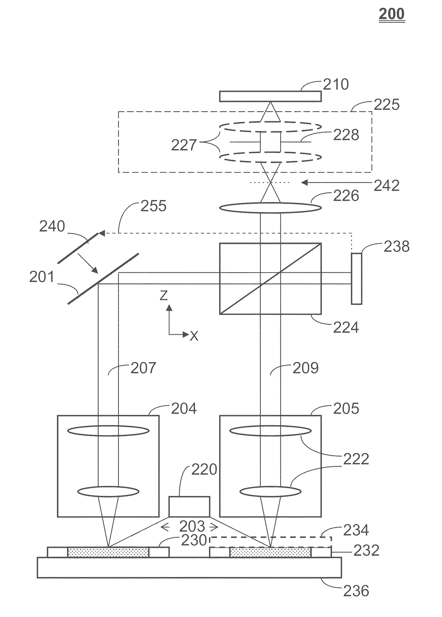
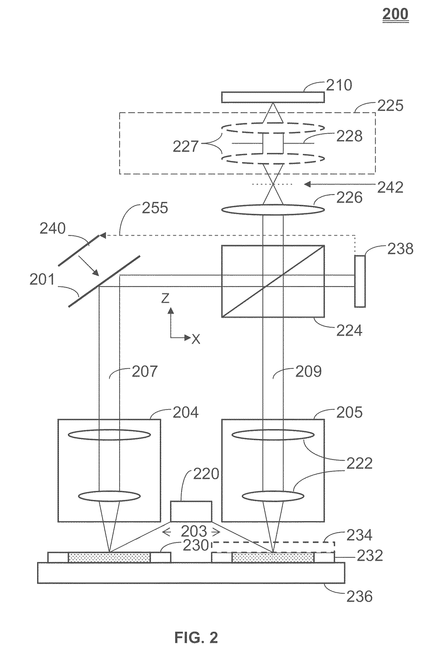
- A reticle inspection system utilizing a coherent illumination source that illuminates both the inspection reticle and a reference reticle, applies Fourier transforms, shifts the phase of the transformed light by 180 degrees, and combines the light to detect differences in amplitude and phase distributions, allowing for the detection of foreign particles and defects using a detector with limited dynamic range.

Reticle inspection with near-field recovery
PatentActiveJP2017523444A
Innovation
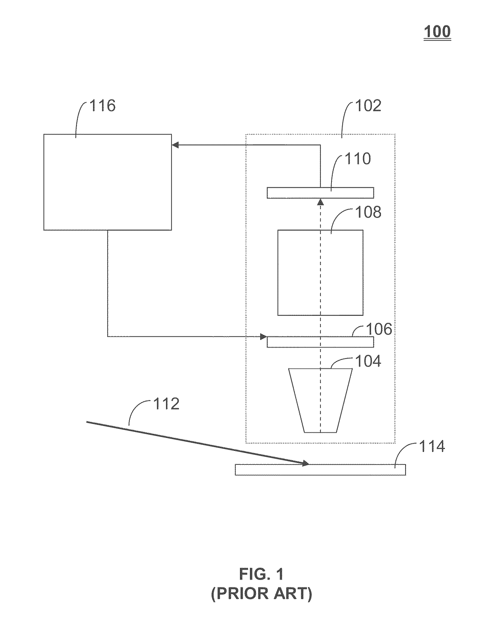
- A computer-implemented method that divides reticle patterns into segments, compares them to a database of predetermined segments using near-field data, and simulates images to detect defects, utilizing near-field recovery techniques to enhance accuracy and efficiency.


Semiconductor Manufacturing Standards and Compliance Requirements
The semiconductor manufacturing industry operates under stringent regulatory frameworks that directly impact advanced reticle inspection technologies for nanometer-level defect detection. International standards organizations, including SEMI, ISO, and IEC, establish comprehensive guidelines governing inspection equipment performance, measurement accuracy, and operational protocols. These standards ensure consistent quality metrics across global manufacturing facilities while maintaining compatibility between different inspection systems and manufacturing processes.
SEMI standards play a pivotal role in defining equipment specifications for reticle inspection systems. SEMI P37 establishes guidelines for reticle defect classification and measurement methodologies, while SEMI P39 specifies requirements for automated defect review systems. These standards mandate specific detection sensitivity thresholds, typically requiring systems to identify defects smaller than 20 nanometers with high confidence levels. Additionally, SEMI E10 defines standard communication protocols between inspection equipment and manufacturing execution systems, ensuring seamless data integration and traceability.
Quality management systems compliance represents another critical aspect of regulatory adherence. ISO 9001 certification requirements extend to reticle inspection processes, demanding documented procedures for calibration, maintenance, and performance verification. Manufacturing facilities must maintain detailed records of inspection results, equipment performance metrics, and corrective actions taken when defects exceed acceptable thresholds. These documentation requirements support continuous improvement initiatives and enable root cause analysis for yield optimization.
Environmental and safety regulations significantly influence inspection system design and operation. Cleanroom standards, particularly ISO 14644, dictate particle contamination limits and airflow requirements that directly affect inspection accuracy. Advanced reticle inspection systems must operate within Class 1 cleanroom environments while minimizing particle generation and electromagnetic interference. Additionally, laser safety regulations govern the use of high-power illumination sources commonly employed in optical inspection systems.
Export control regulations, including the Wassenaar Arrangement and various national security frameworks, impose restrictions on advanced inspection technologies. These regulations classify certain inspection capabilities as dual-use technologies, requiring special licensing for international transfers. Manufacturers must navigate complex compliance requirements when developing systems capable of detecting sub-10 nanometer defects, as such capabilities may fall under strategic technology controls.
Emerging regulatory trends focus on cybersecurity requirements and data protection standards. As inspection systems become increasingly connected and data-driven, compliance with industrial cybersecurity frameworks becomes mandatory. These requirements encompass secure data transmission, access control mechanisms, and protection against cyber threats that could compromise manufacturing operations or intellectual property.
SEMI standards play a pivotal role in defining equipment specifications for reticle inspection systems. SEMI P37 establishes guidelines for reticle defect classification and measurement methodologies, while SEMI P39 specifies requirements for automated defect review systems. These standards mandate specific detection sensitivity thresholds, typically requiring systems to identify defects smaller than 20 nanometers with high confidence levels. Additionally, SEMI E10 defines standard communication protocols between inspection equipment and manufacturing execution systems, ensuring seamless data integration and traceability.
Quality management systems compliance represents another critical aspect of regulatory adherence. ISO 9001 certification requirements extend to reticle inspection processes, demanding documented procedures for calibration, maintenance, and performance verification. Manufacturing facilities must maintain detailed records of inspection results, equipment performance metrics, and corrective actions taken when defects exceed acceptable thresholds. These documentation requirements support continuous improvement initiatives and enable root cause analysis for yield optimization.
Environmental and safety regulations significantly influence inspection system design and operation. Cleanroom standards, particularly ISO 14644, dictate particle contamination limits and airflow requirements that directly affect inspection accuracy. Advanced reticle inspection systems must operate within Class 1 cleanroom environments while minimizing particle generation and electromagnetic interference. Additionally, laser safety regulations govern the use of high-power illumination sources commonly employed in optical inspection systems.
Export control regulations, including the Wassenaar Arrangement and various national security frameworks, impose restrictions on advanced inspection technologies. These regulations classify certain inspection capabilities as dual-use technologies, requiring special licensing for international transfers. Manufacturers must navigate complex compliance requirements when developing systems capable of detecting sub-10 nanometer defects, as such capabilities may fall under strategic technology controls.
Emerging regulatory trends focus on cybersecurity requirements and data protection standards. As inspection systems become increasingly connected and data-driven, compliance with industrial cybersecurity frameworks becomes mandatory. These requirements encompass secure data transmission, access control mechanisms, and protection against cyber threats that could compromise manufacturing operations or intellectual property.
Cost-Benefit Analysis of Advanced Reticle Inspection Implementation
The implementation of advanced reticle inspection systems for nanometer-level defect detection requires substantial capital investment, with high-end EUV reticle inspection tools costing between $15-25 million per unit. However, the economic justification becomes compelling when considering the downstream impact of undetected defects. A single critical defect escaping to wafer production can result in yield losses exceeding $500,000 per lot for advanced semiconductor nodes, making the inspection investment economically viable within months of deployment.
Operational cost analysis reveals that advanced inspection systems consume significant resources through maintenance contracts, typically 10-15% of initial equipment cost annually, specialized consumables, and highly trained operator requirements. Energy consumption for these systems ranges from 50-80 kW during operation, contributing to facility overhead costs. Additionally, the inspection throughput directly impacts fab productivity, with typical inspection times of 2-4 hours per reticle potentially creating bottlenecks in high-volume manufacturing environments.
The quantifiable benefits extend beyond defect detection to include reduced wafer scrapping, improved yield predictability, and enhanced process control capabilities. Statistical analysis indicates that implementing comprehensive reticle inspection can improve overall fab yield by 2-5% for advanced nodes, translating to revenue increases of $10-50 million annually for high-volume facilities. The inspection data also enables predictive maintenance strategies for reticle handling systems and lithography tools, reducing unplanned downtime costs.
Return on investment calculations demonstrate positive outcomes within 12-18 months for most semiconductor manufacturing facilities processing advanced nodes. The break-even point accelerates significantly when factoring in the prevention of catastrophic yield events and the associated customer relationship preservation. Risk mitigation benefits, while harder to quantify, include reduced liability exposure and enhanced reputation protection in the competitive semiconductor market, making advanced reticle inspection a strategically sound investment despite the substantial upfront costs.
Operational cost analysis reveals that advanced inspection systems consume significant resources through maintenance contracts, typically 10-15% of initial equipment cost annually, specialized consumables, and highly trained operator requirements. Energy consumption for these systems ranges from 50-80 kW during operation, contributing to facility overhead costs. Additionally, the inspection throughput directly impacts fab productivity, with typical inspection times of 2-4 hours per reticle potentially creating bottlenecks in high-volume manufacturing environments.
The quantifiable benefits extend beyond defect detection to include reduced wafer scrapping, improved yield predictability, and enhanced process control capabilities. Statistical analysis indicates that implementing comprehensive reticle inspection can improve overall fab yield by 2-5% for advanced nodes, translating to revenue increases of $10-50 million annually for high-volume facilities. The inspection data also enables predictive maintenance strategies for reticle handling systems and lithography tools, reducing unplanned downtime costs.
Return on investment calculations demonstrate positive outcomes within 12-18 months for most semiconductor manufacturing facilities processing advanced nodes. The break-even point accelerates significantly when factoring in the prevention of catastrophic yield events and the associated customer relationship preservation. Risk mitigation benefits, while harder to quantify, include reduced liability exposure and enhanced reputation protection in the competitive semiconductor market, making advanced reticle inspection a strategically sound investment despite the substantial upfront costs.
Unlock deeper insights with Patsnap Eureka Quick Research — get a full tech report to explore trends and direct your research. Try now!
Generate Your Research Report Instantly with AI Agent
Supercharge your innovation with Patsnap Eureka AI Agent Platform!