

Advanced Reticle Inspection vs Wafer-Level Methods for Defect Localization
MAY 20, 20268 MIN READ
Generate Your Research Report Instantly with AI Agent
Patsnap Eureka helps you evaluate technical feasibility & market potential.
Reticle Inspection Technology Background and Objectives
Reticle inspection technology emerged as a critical component of semiconductor manufacturing in the 1980s when photolithography became the dominant patterning method for integrated circuits. As semiconductor devices evolved toward smaller feature sizes and higher integration densities, the quality control of photomasks became paramount to ensuring defect-free wafer production. Early reticle inspection systems relied on optical microscopy and manual examination, which proved inadequate for detecting nanometer-scale defects that could propagate to multiple wafers during the lithography process.
The fundamental principle of reticle inspection involves detecting pattern defects, contamination particles, and dimensional variations on photomasks before they are used in wafer fabrication. Unlike wafer-level inspection that occurs after pattern transfer, reticle inspection serves as a preventive quality control measure, potentially saving thousands of wafers from defective patterning. This upstream approach became increasingly valuable as wafer costs escalated and manufacturing volumes expanded.
Modern reticle inspection technology has evolved to incorporate advanced optical systems, electron beam inspection, and sophisticated image processing algorithms. High-resolution optical inspection systems utilize deep ultraviolet wavelengths and advanced illumination techniques to achieve sub-100nm defect detection capabilities. Electron beam inspection provides even higher resolution but at reduced throughput, making it suitable for critical mask layers and advanced technology nodes.
The primary objective of contemporary reticle inspection technology is to achieve comprehensive defect detection with minimal false positives while maintaining acceptable throughput for high-volume manufacturing. This includes detecting various defect types such as pattern breaks, bridges, dimensional variations, and particle contamination. Advanced systems must also provide accurate defect classification and precise coordinate mapping to enable effective mask repair processes.
As semiconductor technology progresses toward extreme ultraviolet lithography and sub-3nm technology nodes, reticle inspection faces new challenges including actinic inspection requirements, pellicle-related complications, and the need for even higher sensitivity detection. The technology must evolve to support next-generation photomask architectures while maintaining cost-effectiveness and manufacturing efficiency.
The fundamental principle of reticle inspection involves detecting pattern defects, contamination particles, and dimensional variations on photomasks before they are used in wafer fabrication. Unlike wafer-level inspection that occurs after pattern transfer, reticle inspection serves as a preventive quality control measure, potentially saving thousands of wafers from defective patterning. This upstream approach became increasingly valuable as wafer costs escalated and manufacturing volumes expanded.
Modern reticle inspection technology has evolved to incorporate advanced optical systems, electron beam inspection, and sophisticated image processing algorithms. High-resolution optical inspection systems utilize deep ultraviolet wavelengths and advanced illumination techniques to achieve sub-100nm defect detection capabilities. Electron beam inspection provides even higher resolution but at reduced throughput, making it suitable for critical mask layers and advanced technology nodes.
The primary objective of contemporary reticle inspection technology is to achieve comprehensive defect detection with minimal false positives while maintaining acceptable throughput for high-volume manufacturing. This includes detecting various defect types such as pattern breaks, bridges, dimensional variations, and particle contamination. Advanced systems must also provide accurate defect classification and precise coordinate mapping to enable effective mask repair processes.
As semiconductor technology progresses toward extreme ultraviolet lithography and sub-3nm technology nodes, reticle inspection faces new challenges including actinic inspection requirements, pellicle-related complications, and the need for even higher sensitivity detection. The technology must evolve to support next-generation photomask architectures while maintaining cost-effectiveness and manufacturing efficiency.
Market Demand for Advanced Semiconductor Defect Detection
The semiconductor industry faces unprecedented pressure to deliver higher performance chips with smaller feature sizes, driving substantial market demand for advanced defect detection technologies. As manufacturing processes approach atomic-scale precision, traditional inspection methods struggle to identify critical defects that can compromise device functionality and yield rates. This technological gap has created a rapidly expanding market for sophisticated defect detection solutions capable of addressing both reticle-level and wafer-level inspection challenges.
Market growth is primarily fueled by the transition to extreme ultraviolet lithography and advanced node manufacturing below 7nm. These cutting-edge processes require defect detection capabilities that can identify particles, pattern defects, and contamination at unprecedented resolution levels. The increasing complexity of multi-patterning techniques and three-dimensional device architectures further amplifies the need for comprehensive inspection solutions that can operate effectively across different manufacturing stages.
The automotive and consumer electronics sectors represent significant demand drivers, particularly with the proliferation of advanced driver assistance systems, artificial intelligence processors, and high-performance computing applications. These applications demand near-zero defect tolerance, pushing semiconductor manufacturers to invest heavily in both reticle inspection systems and wafer-level detection technologies. The growing emphasis on quality assurance and yield optimization has transformed defect detection from a cost center into a strategic competitive advantage.
Foundry operations worldwide are experiencing intense pressure to maintain high yield rates while reducing manufacturing costs. This economic reality has created strong market pull for inspection technologies that can provide early defect detection, enabling rapid process corrections and minimizing expensive rework. The ability to correlate defects between reticle and wafer levels has become particularly valuable, as it enables root cause analysis and preventive quality management.
Emerging applications in quantum computing, photonics, and advanced packaging technologies are creating new market segments with specialized defect detection requirements. These applications often involve novel materials and unconventional device structures that challenge existing inspection methodologies, driving demand for adaptive and flexible detection platforms capable of handling diverse technological requirements across multiple manufacturing environments.
Market growth is primarily fueled by the transition to extreme ultraviolet lithography and advanced node manufacturing below 7nm. These cutting-edge processes require defect detection capabilities that can identify particles, pattern defects, and contamination at unprecedented resolution levels. The increasing complexity of multi-patterning techniques and three-dimensional device architectures further amplifies the need for comprehensive inspection solutions that can operate effectively across different manufacturing stages.
The automotive and consumer electronics sectors represent significant demand drivers, particularly with the proliferation of advanced driver assistance systems, artificial intelligence processors, and high-performance computing applications. These applications demand near-zero defect tolerance, pushing semiconductor manufacturers to invest heavily in both reticle inspection systems and wafer-level detection technologies. The growing emphasis on quality assurance and yield optimization has transformed defect detection from a cost center into a strategic competitive advantage.
Foundry operations worldwide are experiencing intense pressure to maintain high yield rates while reducing manufacturing costs. This economic reality has created strong market pull for inspection technologies that can provide early defect detection, enabling rapid process corrections and minimizing expensive rework. The ability to correlate defects between reticle and wafer levels has become particularly valuable, as it enables root cause analysis and preventive quality management.
Emerging applications in quantum computing, photonics, and advanced packaging technologies are creating new market segments with specialized defect detection requirements. These applications often involve novel materials and unconventional device structures that challenge existing inspection methodologies, driving demand for adaptive and flexible detection platforms capable of handling diverse technological requirements across multiple manufacturing environments.
Current State of Reticle vs Wafer Inspection Methods
Reticle inspection and wafer-level inspection represent two complementary yet distinct approaches in semiconductor defect detection, each operating at different stages of the manufacturing process with unique technological capabilities and limitations. Reticle inspection focuses on detecting defects on photomasks before they are used in lithography, while wafer-level inspection identifies defects after pattern transfer onto silicon substrates.
Current reticle inspection systems primarily utilize high-resolution optical microscopy and electron beam technologies. Advanced optical systems employ deep ultraviolet wavelengths with numerical apertures exceeding 0.9, enabling detection of defects as small as 20-30 nanometers on advanced photomasks. Electron beam inspection systems offer superior resolution capabilities, reaching sub-10 nanometer sensitivity, but operate at significantly slower throughput rates. Leading platforms integrate multiple detection modes including transmitted light, reflected light, and phase contrast imaging to capture various defect types.
Wafer-level inspection technologies have evolved to address the challenges of detecting defects on patterned wafers with complex three-dimensional structures. Optical wafer inspection systems utilize broadband illumination, laser-based scanning, and advanced image processing algorithms to identify particles, scratches, and pattern defects. These systems typically achieve defect sensitivity in the 15-25 nanometer range for unpatterned wafers and 30-50 nanometers for patterned surfaces, depending on the inspection recipe and pattern density.
The fundamental technological difference lies in inspection environment and target characteristics. Reticle inspection operates on relatively clean, flat chrome-on-glass substrates with well-defined geometric patterns, enabling higher resolution detection algorithms. Wafer inspection must contend with varying topography, multiple material layers, and process-induced variations that create significant noise challenges for defect detection algorithms.
Modern inspection systems increasingly incorporate artificial intelligence and machine learning capabilities to improve defect classification accuracy and reduce false positive rates. Deep learning algorithms trained on extensive defect libraries enable automated distinction between critical defects requiring immediate attention and nuisance defects that may not impact device functionality. This technological advancement has become essential as pattern complexity increases and defect detection sensitivity requirements tighten.
Integration capabilities represent another critical technological aspect, with both reticle and wafer inspection systems requiring seamless connectivity to manufacturing execution systems and yield management platforms. Real-time data analysis and automated defect disposition capabilities have become standard features, enabling rapid feedback loops for process optimization and contamination source identification.
Current reticle inspection systems primarily utilize high-resolution optical microscopy and electron beam technologies. Advanced optical systems employ deep ultraviolet wavelengths with numerical apertures exceeding 0.9, enabling detection of defects as small as 20-30 nanometers on advanced photomasks. Electron beam inspection systems offer superior resolution capabilities, reaching sub-10 nanometer sensitivity, but operate at significantly slower throughput rates. Leading platforms integrate multiple detection modes including transmitted light, reflected light, and phase contrast imaging to capture various defect types.
Wafer-level inspection technologies have evolved to address the challenges of detecting defects on patterned wafers with complex three-dimensional structures. Optical wafer inspection systems utilize broadband illumination, laser-based scanning, and advanced image processing algorithms to identify particles, scratches, and pattern defects. These systems typically achieve defect sensitivity in the 15-25 nanometer range for unpatterned wafers and 30-50 nanometers for patterned surfaces, depending on the inspection recipe and pattern density.
The fundamental technological difference lies in inspection environment and target characteristics. Reticle inspection operates on relatively clean, flat chrome-on-glass substrates with well-defined geometric patterns, enabling higher resolution detection algorithms. Wafer inspection must contend with varying topography, multiple material layers, and process-induced variations that create significant noise challenges for defect detection algorithms.
Modern inspection systems increasingly incorporate artificial intelligence and machine learning capabilities to improve defect classification accuracy and reduce false positive rates. Deep learning algorithms trained on extensive defect libraries enable automated distinction between critical defects requiring immediate attention and nuisance defects that may not impact device functionality. This technological advancement has become essential as pattern complexity increases and defect detection sensitivity requirements tighten.
Integration capabilities represent another critical technological aspect, with both reticle and wafer inspection systems requiring seamless connectivity to manufacturing execution systems and yield management platforms. Real-time data analysis and automated defect disposition capabilities have become standard features, enabling rapid feedback loops for process optimization and contamination source identification.
Existing Reticle and Wafer-Level Inspection Solutions
01 Machine learning and AI-based defect detection methods
Advanced machine learning algorithms and artificial intelligence techniques are employed to automatically identify and classify defects in various materials and products. These methods utilize neural networks, deep learning models, and pattern recognition algorithms to analyze images or sensor data and detect anomalies with high accuracy. The systems can be trained on large datasets to improve detection performance and reduce false positives.- Machine learning and AI-based defect detection methods: Advanced machine learning algorithms and artificial intelligence techniques are employed to automatically identify and localize defects in various systems. These methods utilize neural networks, deep learning models, and pattern recognition algorithms to analyze data and detect anomalies with high accuracy. The AI-based approaches can learn from training datasets to improve detection performance and reduce false positives in defect identification processes.
- Image processing and computer vision techniques for defect localization: Computer vision and image processing methodologies are utilized to analyze visual data for defect detection and precise localization. These techniques involve image enhancement, feature extraction, edge detection, and morphological operations to identify defective areas. Advanced imaging algorithms process captured images to highlight defects and provide accurate spatial coordinates of detected anomalies.
- Statistical analysis and signal processing methods: Statistical approaches and signal processing techniques are applied to analyze measurement data and identify deviations from normal patterns. These methods involve statistical modeling, threshold-based detection, frequency domain analysis, and time-series analysis to detect defects. The statistical frameworks help in establishing baseline parameters and detecting anomalies that exceed predefined tolerance limits.
- Multi-sensor fusion and hybrid detection systems: Integration of multiple sensing technologies and detection methods to enhance defect localization accuracy through data fusion. These systems combine information from various sensors such as optical, thermal, ultrasonic, and electromagnetic sensors to provide comprehensive defect analysis. The hybrid approach leverages the strengths of different detection modalities to achieve superior accuracy and reliability in defect identification.
- Real-time monitoring and automated inspection systems: Continuous monitoring systems that provide real-time defect detection and localization capabilities for industrial applications. These automated inspection systems incorporate high-speed processing algorithms and real-time data analysis to detect defects during manufacturing or operational processes. The systems enable immediate feedback and corrective actions to maintain quality standards and prevent defective products from progressing through production lines.
02 Image processing and computer vision techniques
Computer vision algorithms and image processing methods are used to analyze visual data for defect identification. These techniques include edge detection, feature extraction, morphological operations, and statistical analysis of image characteristics. The methods can process high-resolution images in real-time to identify surface defects, dimensional variations, and other visual anomalies with enhanced precision.Expand Specific Solutions03 Multi-sensor fusion and data integration approaches
Integration of multiple sensing technologies and data sources to improve defect detection accuracy and reliability. These approaches combine information from various sensors such as optical, thermal, ultrasonic, and electromagnetic devices to provide comprehensive defect analysis. The fusion of different data types enables better characterization of defects and reduces detection uncertainties.Expand Specific Solutions04 Statistical analysis and signal processing methods
Mathematical and statistical techniques for analyzing measurement data and signals to identify defect patterns and anomalies. These methods include time-frequency analysis, correlation analysis, hypothesis testing, and statistical process control. The approaches help in distinguishing between normal variations and actual defects by establishing statistical thresholds and confidence intervals.Expand Specific Solutions05 Automated inspection systems and real-time monitoring
Comprehensive automated inspection platforms that provide continuous monitoring and real-time defect detection capabilities. These systems integrate hardware components, software algorithms, and user interfaces to enable efficient quality control processes. The platforms can be customized for specific applications and provide detailed reporting and analysis of detected defects.Expand Specific Solutions
Key Players in Semiconductor Inspection Equipment
The advanced reticle inspection versus wafer-level defect localization market represents a mature yet rapidly evolving segment within semiconductor manufacturing, driven by increasing demand for sub-nanometer precision in advanced node production. The industry is experiencing significant growth with market valuations exceeding several billion dollars annually, fueled by AI, 5G, and automotive semiconductor requirements. Technology maturity varies significantly across players, with established leaders like KLA Corp., Applied Materials, and Tokyo Electron demonstrating advanced capabilities in both reticle and wafer-level inspection systems. Emerging competitors including Skyverse Technology, Wuxi Zhuohai Technology, and Dongfang Jingyuan Electron are developing specialized solutions, while foundry giants Samsung Electronics, GLOBALFOUNDRIES, and United Microelectronics drive demand through advanced manufacturing requirements. The competitive landscape shows consolidation around comprehensive inspection platforms integrating AI-driven defect classification and real-time process control capabilities.
KLA Corp.
Technical Solution: KLA Corporation leads in advanced reticle inspection with their 5XX series reticle inspection systems, featuring high-resolution optical and e-beam inspection capabilities. Their technology combines brightfield, darkfield, and transmitted light inspection modes with advanced defect classification algorithms. For wafer-level defect localization, KLA offers integrated solutions that correlate reticle defects with wafer printing results through their advanced pattern recognition and machine learning algorithms. The company's inspection systems can detect defects as small as 20nm on reticles and provide precise coordinate mapping to wafer locations. Their technology stack includes advanced optics, high-speed scanning mechanisms, and sophisticated image processing software that enables real-time defect detection and classification during semiconductor manufacturing processes.
Strengths: Industry-leading detection sensitivity and accuracy, comprehensive defect classification capabilities, strong integration with fab workflows. Weaknesses: High equipment cost and complexity, requires specialized operator training and maintenance expertise.
Applied Materials, Inc.
Technical Solution: Applied Materials provides comprehensive defect inspection solutions through their PROVision platform, which integrates both reticle and wafer-level inspection capabilities. Their advanced reticle inspection systems utilize multi-beam e-beam technology and high-resolution optical inspection to detect critical defects on photomasks. The company's wafer-level defect localization approach combines their SEMVision G7 review SEM with advanced pattern recognition algorithms to precisely locate and classify defects transferred from reticles to wafers. Their integrated workflow enables automatic defect coordinate transformation between reticle and wafer coordinate systems, facilitating rapid root cause analysis. The platform incorporates machine learning algorithms for improved defect classification accuracy and reduced false positive rates, while providing comprehensive defect trending and yield impact analysis capabilities for semiconductor manufacturers.
Strengths: Comprehensive integrated platform covering entire inspection workflow, strong machine learning capabilities for defect classification, excellent fab integration. Weaknesses: Complex system integration requirements, significant capital investment needed for full platform deployment.
Core Innovations in Advanced Defect Localization
Method and system for controlling the quality of a reticle
PatentWO2005073806A1
Innovation
- A method and system that directly assess the printing defects of a reticle by comparing reference and test data sets obtained from patterns produced using the reticle at different times, focusing on radiation responses to incident radiation, and using this analysis to generate output data indicative of the reticle's current condition, allowing for the detection of defects that would otherwise be missed.


Methods and systems for classifying defects detected on a reticle
PatentActiveUS8204297B1
Innovation
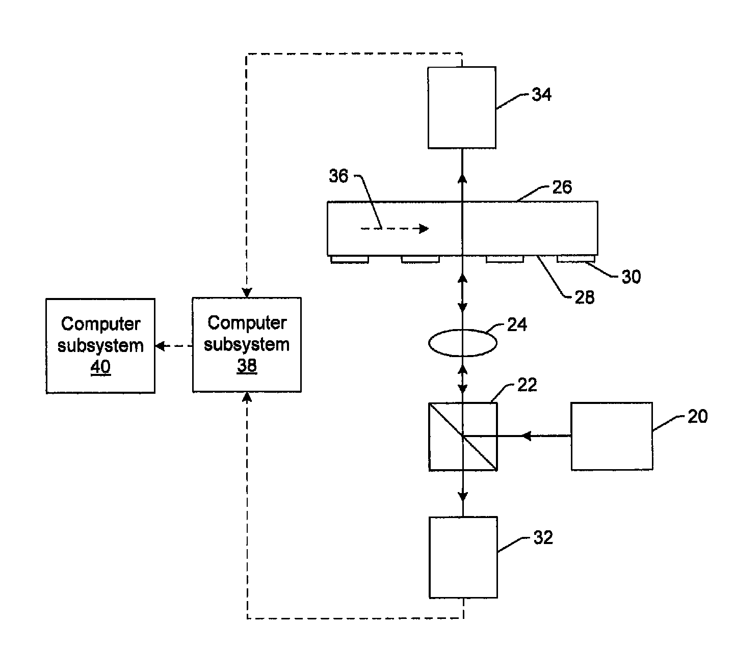
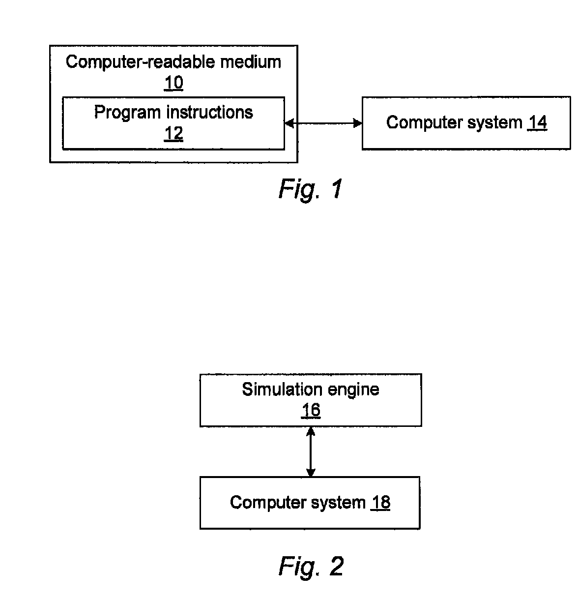
- A method and system that classify defects on a reticle by determining their impact on the performance of a device being fabricated on a wafer, using simulated or aerial images to assess how the defect will print, and assigning a classification to guide review and repair decisions.


Semiconductor Manufacturing Quality Standards
Semiconductor manufacturing quality standards represent a comprehensive framework of specifications, protocols, and metrics that govern the production of integrated circuits and related components. These standards encompass multiple dimensions of quality control, including defect density thresholds, yield requirements, reliability specifications, and process capability indices that collectively ensure the delivery of high-performance semiconductor products to market.
The International Technology Roadmap for Semiconductors (ITRS) and its successor, the International Roadmap for Devices and Systems (IRDS), establish fundamental quality benchmarks that drive industry-wide adoption of advanced inspection methodologies. Current standards mandate defect densities below 0.1 defects per square centimeter for critical layers in advanced nodes, with zero tolerance for killer defects that could compromise device functionality or reliability.
Quality standards specifically addressing defect localization emphasize the criticality of detection accuracy, false positive rates, and throughput requirements. Advanced reticle inspection systems must demonstrate detection capabilities for defects as small as 20-30 nanometers, while maintaining false alarm rates below 10 parts per million to ensure manufacturing efficiency. These specifications directly influence the comparative evaluation of reticle-level versus wafer-level inspection approaches.
Wafer-level quality standards focus on in-line monitoring capabilities, requiring real-time defect classification and disposition decisions within manufacturing cycle time constraints. Standards mandate 100% wafer inspection coverage for critical process steps, with defect localization accuracy within 50 nanometers for advanced technology nodes. This precision requirement drives the development of hybrid inspection strategies that leverage both reticle and wafer-level methodologies.
Emerging quality standards incorporate machine learning-based defect classification requirements, mandating minimum confidence levels of 95% for automated defect dispositioning. These evolving standards recognize the increasing complexity of defect signatures in advanced semiconductor manufacturing processes and the need for intelligent inspection systems that can adapt to new defect types and process variations while maintaining stringent quality control objectives.
The International Technology Roadmap for Semiconductors (ITRS) and its successor, the International Roadmap for Devices and Systems (IRDS), establish fundamental quality benchmarks that drive industry-wide adoption of advanced inspection methodologies. Current standards mandate defect densities below 0.1 defects per square centimeter for critical layers in advanced nodes, with zero tolerance for killer defects that could compromise device functionality or reliability.
Quality standards specifically addressing defect localization emphasize the criticality of detection accuracy, false positive rates, and throughput requirements. Advanced reticle inspection systems must demonstrate detection capabilities for defects as small as 20-30 nanometers, while maintaining false alarm rates below 10 parts per million to ensure manufacturing efficiency. These specifications directly influence the comparative evaluation of reticle-level versus wafer-level inspection approaches.
Wafer-level quality standards focus on in-line monitoring capabilities, requiring real-time defect classification and disposition decisions within manufacturing cycle time constraints. Standards mandate 100% wafer inspection coverage for critical process steps, with defect localization accuracy within 50 nanometers for advanced technology nodes. This precision requirement drives the development of hybrid inspection strategies that leverage both reticle and wafer-level methodologies.
Emerging quality standards incorporate machine learning-based defect classification requirements, mandating minimum confidence levels of 95% for automated defect dispositioning. These evolving standards recognize the increasing complexity of defect signatures in advanced semiconductor manufacturing processes and the need for intelligent inspection systems that can adapt to new defect types and process variations while maintaining stringent quality control objectives.
Cost-Benefit Analysis of Inspection Method Selection
The selection between advanced reticle inspection and wafer-level methods for defect localization requires comprehensive cost-benefit evaluation across multiple dimensions. Initial capital expenditure represents a significant differentiator, with advanced reticle inspection systems typically requiring investments ranging from $15-30 million per tool, while wafer-level inspection equipment generally costs $8-20 million depending on resolution requirements and throughput specifications.
Operational cost structures reveal distinct patterns between methodologies. Reticle inspection demonstrates superior cost efficiency in high-volume manufacturing scenarios, where single reticle defects can impact thousands of wafers. The cost per defect detection at reticle level averages $0.50-2.00, compared to $5.00-15.00 per defect at wafer level when accounting for processing costs and yield loss propagation.
Throughput considerations significantly influence total cost of ownership calculations. Advanced reticle inspection systems achieve inspection rates of 200-500 reticles per day with sub-20nm defect sensitivity, while wafer-level methods process 50-150 wafers daily at comparable resolution. However, the multiplicative effect of reticle defects necessitates different weighting factors in throughput analysis.
Yield impact assessment reveals critical economic implications. Reticle-level defect detection prevents systematic yield loss across entire production lots, potentially saving $500,000-2,000,000 per critical defect caught early. Conversely, wafer-level detection enables identification of process-induced defects and random failures that reticle inspection cannot capture, providing complementary value in yield optimization strategies.
Return on investment calculations demonstrate technology-dependent optimization points. For advanced node production below 7nm, reticle inspection typically achieves ROI within 18-24 months due to high wafer values and defect sensitivity requirements. Mature node manufacturing often favors wafer-level approaches, achieving ROI in 12-18 months through higher throughput and lower complexity requirements.
Risk mitigation costs must factor into selection criteria, including false positive rates, detection capability gaps, and integration complexity with existing manufacturing execution systems.
Operational cost structures reveal distinct patterns between methodologies. Reticle inspection demonstrates superior cost efficiency in high-volume manufacturing scenarios, where single reticle defects can impact thousands of wafers. The cost per defect detection at reticle level averages $0.50-2.00, compared to $5.00-15.00 per defect at wafer level when accounting for processing costs and yield loss propagation.
Throughput considerations significantly influence total cost of ownership calculations. Advanced reticle inspection systems achieve inspection rates of 200-500 reticles per day with sub-20nm defect sensitivity, while wafer-level methods process 50-150 wafers daily at comparable resolution. However, the multiplicative effect of reticle defects necessitates different weighting factors in throughput analysis.
Yield impact assessment reveals critical economic implications. Reticle-level defect detection prevents systematic yield loss across entire production lots, potentially saving $500,000-2,000,000 per critical defect caught early. Conversely, wafer-level detection enables identification of process-induced defects and random failures that reticle inspection cannot capture, providing complementary value in yield optimization strategies.
Return on investment calculations demonstrate technology-dependent optimization points. For advanced node production below 7nm, reticle inspection typically achieves ROI within 18-24 months due to high wafer values and defect sensitivity requirements. Mature node manufacturing often favors wafer-level approaches, achieving ROI in 12-18 months through higher throughput and lower complexity requirements.
Risk mitigation costs must factor into selection criteria, including false positive rates, detection capability gaps, and integration complexity with existing manufacturing execution systems.
Unlock deeper insights with Patsnap Eureka Quick Research — get a full tech report to explore trends and direct your research. Try now!
Generate Your Research Report Instantly with AI Agent
Supercharge your innovation with Patsnap Eureka AI Agent Platform!