

Quantify Reflective Index Variations Using Advanced Reticle Inspection Tools
MAY 20, 20269 MIN READ
Generate Your Research Report Instantly with AI Agent
Patsnap Eureka helps you evaluate technical feasibility & market potential.
Reticle Inspection Technology Background and Objectives
Reticle inspection technology has emerged as a critical component in semiconductor manufacturing, driven by the relentless pursuit of smaller feature sizes and higher device densities. As integrated circuits continue to shrink according to Moore's Law, the precision requirements for photolithography masks have reached unprecedented levels. Traditional inspection methods, while effective for larger geometries, face significant limitations when detecting nanometer-scale defects that can critically impact device performance and yield.
The evolution of reticle inspection systems has been closely tied to advances in optical imaging, computational algorithms, and sensor technologies. Early inspection tools relied primarily on brightfield and darkfield optical microscopy, which provided adequate resolution for feature sizes above 100 nanometers. However, as critical dimensions approached the wavelength of visible light, these conventional approaches became insufficient for detecting subtle variations in refractive index that could indicate material inconsistencies or structural defects.
Advanced reticle inspection tools now incorporate sophisticated optical configurations, including high-numerical-aperture objectives, coherent illumination systems, and multi-wavelength analysis capabilities. These systems enable the quantification of minute variations in optical properties that were previously undetectable. The integration of machine learning algorithms and artificial intelligence has further enhanced the sensitivity and accuracy of defect detection, allowing for real-time analysis of complex optical signatures.
The primary objective of quantifying reflective index variations using advanced inspection tools is to establish a comprehensive understanding of mask quality that extends beyond simple geometric measurements. This approach enables manufacturers to identify potential failure modes before they impact production yields, thereby reducing costly rework and improving overall manufacturing efficiency.
Current technological goals focus on achieving sub-nanometer sensitivity in refractive index measurements while maintaining high throughput rates compatible with production environments. The development of next-generation inspection systems aims to provide three-dimensional characterization of mask structures, enabling detection of buried defects and material inhomogeneities that could affect optical performance during lithography processes.
Furthermore, the integration of predictive analytics capabilities represents a significant advancement in reticle inspection technology. By correlating measured refractive index variations with downstream lithographic performance, these systems can provide early warning indicators of potential yield issues, enabling proactive quality management strategies that minimize production disruptions and optimize manufacturing outcomes.
The evolution of reticle inspection systems has been closely tied to advances in optical imaging, computational algorithms, and sensor technologies. Early inspection tools relied primarily on brightfield and darkfield optical microscopy, which provided adequate resolution for feature sizes above 100 nanometers. However, as critical dimensions approached the wavelength of visible light, these conventional approaches became insufficient for detecting subtle variations in refractive index that could indicate material inconsistencies or structural defects.
Advanced reticle inspection tools now incorporate sophisticated optical configurations, including high-numerical-aperture objectives, coherent illumination systems, and multi-wavelength analysis capabilities. These systems enable the quantification of minute variations in optical properties that were previously undetectable. The integration of machine learning algorithms and artificial intelligence has further enhanced the sensitivity and accuracy of defect detection, allowing for real-time analysis of complex optical signatures.
The primary objective of quantifying reflective index variations using advanced inspection tools is to establish a comprehensive understanding of mask quality that extends beyond simple geometric measurements. This approach enables manufacturers to identify potential failure modes before they impact production yields, thereby reducing costly rework and improving overall manufacturing efficiency.
Current technological goals focus on achieving sub-nanometer sensitivity in refractive index measurements while maintaining high throughput rates compatible with production environments. The development of next-generation inspection systems aims to provide three-dimensional characterization of mask structures, enabling detection of buried defects and material inhomogeneities that could affect optical performance during lithography processes.
Furthermore, the integration of predictive analytics capabilities represents a significant advancement in reticle inspection technology. By correlating measured refractive index variations with downstream lithographic performance, these systems can provide early warning indicators of potential yield issues, enabling proactive quality management strategies that minimize production disruptions and optimize manufacturing outcomes.
Market Demand for Advanced Reticle Inspection Solutions
The semiconductor industry's relentless pursuit of smaller node technologies has created an unprecedented demand for advanced reticle inspection solutions capable of quantifying reflective index variations. As chip manufacturers transition to extreme ultraviolet lithography and sub-3nm processes, the tolerance for reticle defects has decreased exponentially, driving the need for more sophisticated inspection capabilities that can detect and measure minute variations in optical properties.
Traditional reticle inspection methods are increasingly inadequate for next-generation semiconductor manufacturing requirements. The industry faces mounting pressure to identify defects at the nanometer scale while maintaining high throughput production schedules. This challenge has intensified the market demand for inspection tools that can precisely quantify reflective index variations, as these measurements directly correlate with lithographic performance and yield optimization.
Leading semiconductor foundries and integrated device manufacturers are actively seeking inspection solutions that combine high-resolution imaging with advanced optical analysis capabilities. The market demand is particularly strong for tools that can provide real-time feedback on reticle quality, enabling immediate corrective actions during the manufacturing process. This requirement has shifted the focus from simple defect detection to comprehensive optical characterization.
The emergence of artificial intelligence and machine learning technologies has further amplified market expectations for advanced reticle inspection systems. Customers increasingly demand solutions that can not only quantify reflective index variations but also predict their impact on final device performance. This predictive capability represents a significant value proposition for manufacturers seeking to optimize their production processes and reduce costly rework cycles.
Market demand is also driven by the expanding application scope beyond traditional logic and memory devices. The growing importance of specialized semiconductors for automotive, aerospace, and quantum computing applications has created new requirements for reticle inspection precision. These emerging markets often require custom specifications and enhanced measurement capabilities, further expanding the addressable market for advanced inspection solutions.
The competitive landscape has intensified as equipment suppliers race to meet these evolving market demands. Companies are investing heavily in research and development to deliver inspection tools that can quantify reflective index variations with unprecedented accuracy and speed. This investment cycle reflects the substantial market opportunity and the critical importance of reticle quality in modern semiconductor manufacturing.
Traditional reticle inspection methods are increasingly inadequate for next-generation semiconductor manufacturing requirements. The industry faces mounting pressure to identify defects at the nanometer scale while maintaining high throughput production schedules. This challenge has intensified the market demand for inspection tools that can precisely quantify reflective index variations, as these measurements directly correlate with lithographic performance and yield optimization.
Leading semiconductor foundries and integrated device manufacturers are actively seeking inspection solutions that combine high-resolution imaging with advanced optical analysis capabilities. The market demand is particularly strong for tools that can provide real-time feedback on reticle quality, enabling immediate corrective actions during the manufacturing process. This requirement has shifted the focus from simple defect detection to comprehensive optical characterization.
The emergence of artificial intelligence and machine learning technologies has further amplified market expectations for advanced reticle inspection systems. Customers increasingly demand solutions that can not only quantify reflective index variations but also predict their impact on final device performance. This predictive capability represents a significant value proposition for manufacturers seeking to optimize their production processes and reduce costly rework cycles.
Market demand is also driven by the expanding application scope beyond traditional logic and memory devices. The growing importance of specialized semiconductors for automotive, aerospace, and quantum computing applications has created new requirements for reticle inspection precision. These emerging markets often require custom specifications and enhanced measurement capabilities, further expanding the addressable market for advanced inspection solutions.
The competitive landscape has intensified as equipment suppliers race to meet these evolving market demands. Companies are investing heavily in research and development to deliver inspection tools that can quantify reflective index variations with unprecedented accuracy and speed. This investment cycle reflects the substantial market opportunity and the critical importance of reticle quality in modern semiconductor manufacturing.
Current State of Reflective Index Quantification Methods
Reflective index quantification in semiconductor manufacturing has evolved significantly over the past decade, driven by the increasing complexity of advanced lithography processes. Current methodologies primarily rely on optical measurement techniques integrated within reticle inspection systems, utilizing spectroscopic ellipsometry and interferometry principles to detect minute variations in material properties across photomask surfaces.
The predominant approach involves multi-wavelength optical systems that capture reflectance data across ultraviolet to near-infrared spectrums. These systems employ sophisticated algorithms to correlate measured optical signatures with underlying material characteristics, enabling detection of reflective index variations as small as 0.001 units. Advanced signal processing techniques, including machine learning algorithms, have been integrated to enhance measurement accuracy and reduce noise interference.
Scatterometry-based methods represent another significant advancement in current quantification approaches. These techniques analyze diffracted light patterns from periodic structures on reticles, providing detailed information about material composition and thickness variations that directly influence reflective properties. The integration of polarized light sources and advanced detector arrays has substantially improved measurement sensitivity and spatial resolution.
Phase-shifting interferometry has emerged as a critical technique for high-precision reflective index mapping. This method leverages controlled phase variations in incident light to generate detailed topographical and optical property maps across reticle surfaces. Modern implementations utilize adaptive optics and real-time calibration systems to compensate for environmental fluctuations and systematic measurement errors.
Contemporary inspection tools incorporate hybrid measurement approaches, combining multiple optical techniques within single platforms. These integrated systems enable cross-validation of measurements and provide comprehensive characterization of reflective properties across different spatial scales. Advanced data fusion algorithms process information from multiple measurement channels to generate robust quantification results.
Current limitations include measurement speed constraints for high-resolution mapping applications and challenges in quantifying reflective properties of novel materials used in next-generation photomasks. Additionally, the complexity of modern multilayer reticle structures presents ongoing challenges for accurate depth-resolved reflective index characterization, particularly in extreme ultraviolet lithography applications where material properties exhibit strong wavelength dependencies.
The predominant approach involves multi-wavelength optical systems that capture reflectance data across ultraviolet to near-infrared spectrums. These systems employ sophisticated algorithms to correlate measured optical signatures with underlying material characteristics, enabling detection of reflective index variations as small as 0.001 units. Advanced signal processing techniques, including machine learning algorithms, have been integrated to enhance measurement accuracy and reduce noise interference.
Scatterometry-based methods represent another significant advancement in current quantification approaches. These techniques analyze diffracted light patterns from periodic structures on reticles, providing detailed information about material composition and thickness variations that directly influence reflective properties. The integration of polarized light sources and advanced detector arrays has substantially improved measurement sensitivity and spatial resolution.
Phase-shifting interferometry has emerged as a critical technique for high-precision reflective index mapping. This method leverages controlled phase variations in incident light to generate detailed topographical and optical property maps across reticle surfaces. Modern implementations utilize adaptive optics and real-time calibration systems to compensate for environmental fluctuations and systematic measurement errors.
Contemporary inspection tools incorporate hybrid measurement approaches, combining multiple optical techniques within single platforms. These integrated systems enable cross-validation of measurements and provide comprehensive characterization of reflective properties across different spatial scales. Advanced data fusion algorithms process information from multiple measurement channels to generate robust quantification results.
Current limitations include measurement speed constraints for high-resolution mapping applications and challenges in quantifying reflective properties of novel materials used in next-generation photomasks. Additionally, the complexity of modern multilayer reticle structures presents ongoing challenges for accurate depth-resolved reflective index characterization, particularly in extreme ultraviolet lithography applications where material properties exhibit strong wavelength dependencies.
Existing Advanced Reticle Inspection Solutions
01 Optical measurement systems for reticle inspection
Advanced optical measurement systems are employed to detect and analyze reflective index variations in reticles. These systems utilize sophisticated light sources and detection mechanisms to identify defects, contamination, and structural irregularities that affect the refractive properties of photomasks. The measurement techniques enable precise characterization of optical properties across different regions of the reticle surface.- Optical measurement systems for reticle inspection: Advanced optical measurement systems are employed to detect and analyze reflective index variations in reticles. These systems utilize sophisticated light sources and detection mechanisms to identify defects, contamination, and structural irregularities that affect the refractive properties of reticle materials. The measurement systems can operate across multiple wavelengths and provide high-resolution analysis of optical characteristics.
- Image processing algorithms for defect detection: Specialized image processing and pattern recognition algorithms are developed to automatically identify and classify reflective index variations in reticle inspection data. These algorithms can distinguish between acceptable variations and critical defects by analyzing optical signatures, intensity patterns, and spatial distributions of reflective properties across the reticle surface.
- Multi-wavelength inspection techniques: Multi-wavelength inspection methods are utilized to comprehensively analyze reflective index variations by examining reticles under different illumination conditions. These techniques enable the detection of wavelength-dependent optical properties and provide enhanced sensitivity to various types of defects that may not be visible under single-wavelength inspection.
- Calibration and reference standards for accurate measurement: Precise calibration methods and reference standards are essential for maintaining measurement accuracy in reticle inspection systems. These approaches involve the use of certified reference materials, standardized measurement protocols, and compensation techniques to account for systematic variations in reflective index measurements and ensure consistent results across different inspection tools.
- Real-time monitoring and feedback control systems: Real-time monitoring systems are implemented to continuously track reflective index variations during reticle inspection processes. These systems provide immediate feedback and can trigger corrective actions when variations exceed predetermined thresholds, ensuring consistent quality control and enabling rapid response to process deviations.
02 Image processing algorithms for defect detection
Specialized image processing and analysis algorithms are developed to identify reflective index variations through pattern recognition and comparative analysis. These computational methods process captured optical data to distinguish between normal reticle features and anomalies that indicate refractive index deviations. The algorithms enhance detection sensitivity and reduce false positive rates in inspection processes.Expand Specific Solutions03 Multi-wavelength inspection techniques
Multi-wavelength optical inspection methods are utilized to comprehensively analyze reflective index variations across different spectral ranges. These techniques employ various light wavelengths to reveal refractive index changes that may not be visible under single-wavelength illumination. The approach provides enhanced detection capabilities for subtle variations in optical properties of reticle materials.Expand Specific Solutions04 Calibration and reference standards for accurate measurement
Precise calibration methodologies and reference standards are established to ensure accurate measurement of reflective index variations. These systems incorporate known optical standards and calibration procedures to maintain measurement accuracy and repeatability across different inspection tools. The calibration processes account for environmental factors and instrument drift that could affect measurement precision.Expand Specific Solutions05 Real-time monitoring and feedback systems
Real-time monitoring systems are implemented to continuously track reflective index variations during reticle inspection processes. These systems provide immediate feedback on optical property changes and enable dynamic adjustment of inspection parameters. The monitoring capabilities facilitate rapid detection of process deviations and support quality control in semiconductor manufacturing environments.Expand Specific Solutions
Key Players in Reticle Inspection Equipment Industry
The quantification of reflective index variations using advanced reticle inspection tools represents a mature technology segment within the semiconductor lithography ecosystem, currently experiencing steady growth driven by increasing demand for precision in advanced node manufacturing. The market demonstrates significant scale, with established players like ASML Netherlands BV, Canon Inc., and Nikon Corp. dominating lithography equipment, while companies such as Carl Zeiss SMT GmbH provide critical optical components. Technology maturity varies across the competitive landscape, with ASML leading in EUV lithography capabilities, Taiwan Semiconductor Manufacturing Co. driving foundry-level implementation requirements, and emerging players like Shanghai Microelectronics Equipment Group developing competitive solutions. Research institutions including Technical University of Denmark and Fraunhofer-Gesellschaft contribute fundamental research, while materials suppliers like DuPont de Nemours and AGC Inc. support the ecosystem with specialized substrates and optical materials essential for precise reticle inspection applications.
Canon, Inc.
Technical Solution: Canon implements advanced optical inspection technologies in their reticle inspection systems, utilizing proprietary imaging sensors and computational optics to detect and quantify reflective index variations across photomask surfaces. Their approach combines high-resolution optical microscopy with spectroscopic analysis techniques to measure material properties and surface characteristics that affect reflective behavior. Canon's inspection methodology includes automated pattern matching algorithms, statistical analysis tools, and defect classification systems that enable precise quantification of optical property variations, supporting quality control processes in semiconductor photomask manufacturing and ensuring optimal lithographic performance in production environments.
Strengths: Advanced imaging technology, cost-effective solutions, reliable optical systems. Weaknesses: Limited market share in high-end inspection, less comprehensive software ecosystem, slower adoption of cutting-edge technologies.
Applied Materials Israel Ltd.
Technical Solution: Applied Materials develops comprehensive reticle inspection platforms that integrate multiple detection technologies including brightfield and darkfield optical inspection, electron beam inspection, and advanced image analysis algorithms to quantify reflective index variations. Their systems employ proprietary defect detection algorithms and statistical process control methods to monitor and measure variations in reticle optical properties throughout the manufacturing process. The company's inspection solutions feature automated defect classification, trend analysis capabilities, and integration with fab-wide process control systems, enabling real-time monitoring and correction of reflective index deviations that could impact lithographic performance and yield.
Strengths: Comprehensive inspection capabilities, strong process integration, extensive industry experience. Weaknesses: Complex system integration requirements, high maintenance costs, steep learning curve for operators.
Core Innovations in Reflective Index Measurement
Apparatus and methods for inspecting reticles
PatentActiveUS20180082415A1
Innovation
- A method and system for qualifying photolithographic reticles by acquiring images at different illumination and imaging configurations to recover the reticle near field, which is then analyzed to determine potential wafer pattern defects and stability, using a lithography model to simulate wafer images and compare them under various process conditions.


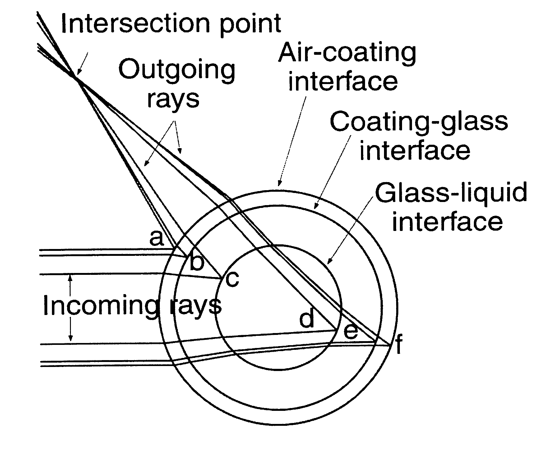
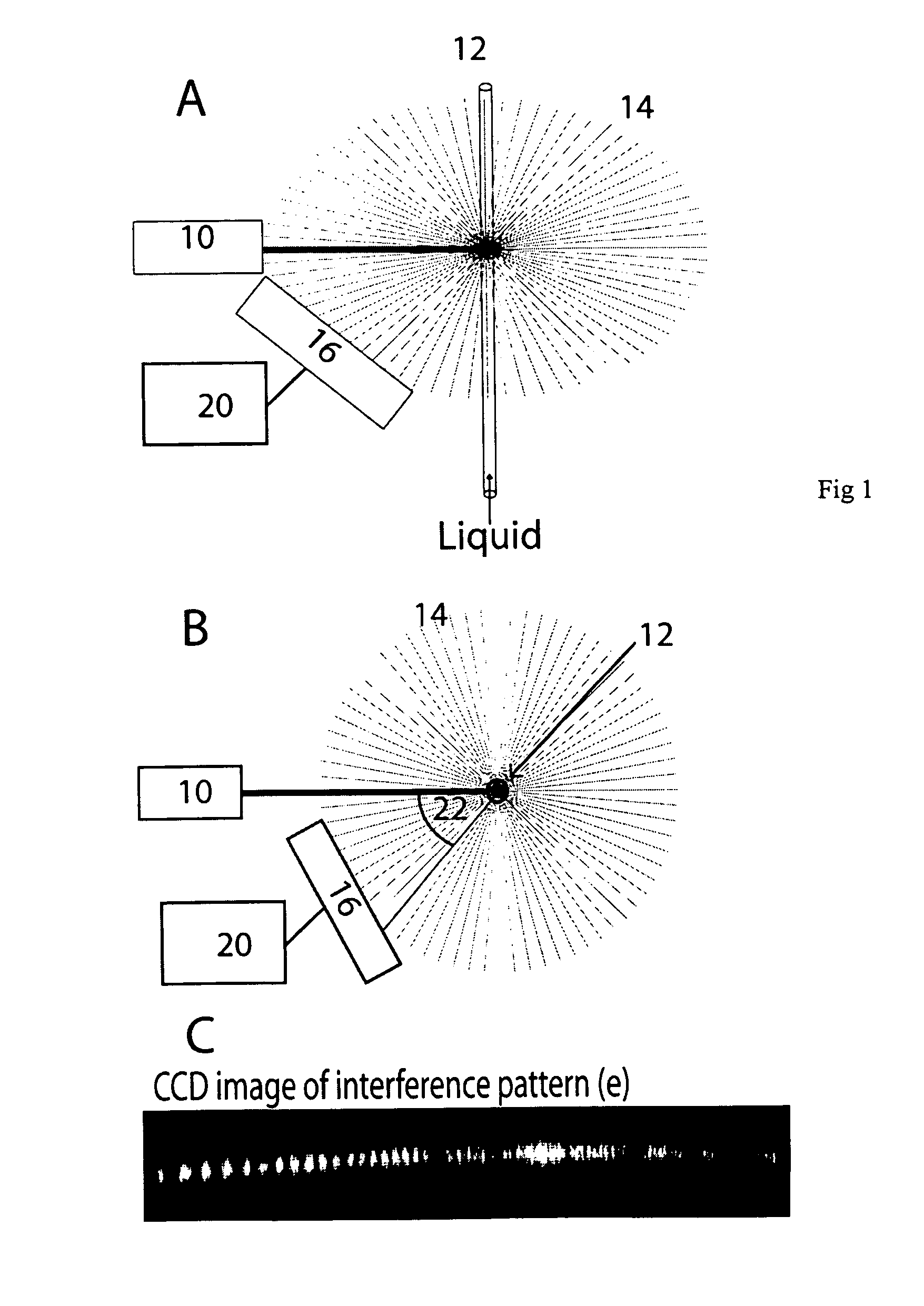
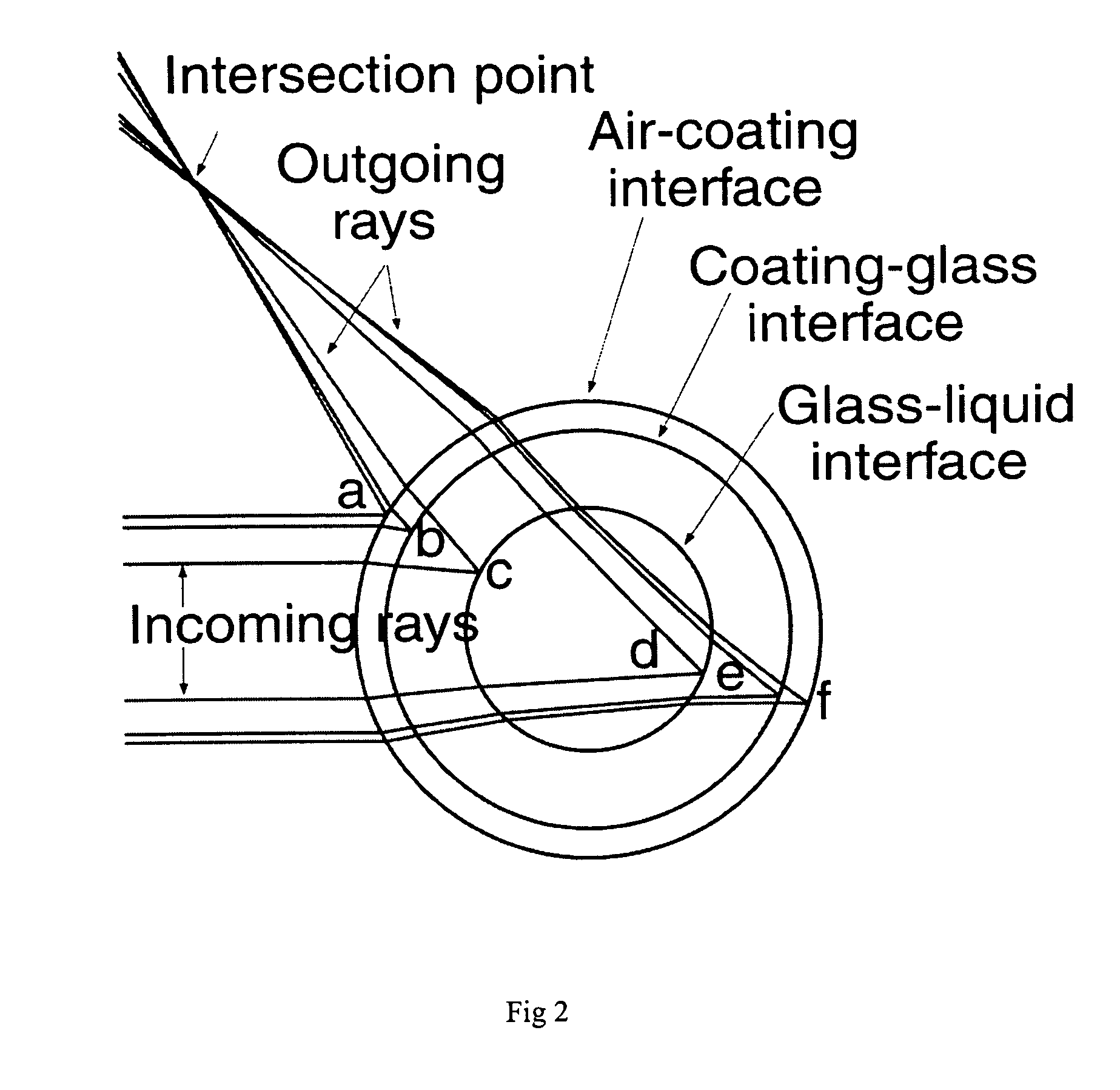
Refractive index determination by micro interferometric reflection detection
PatentInactiveUS7130060B2
Innovation
- The method involves analyzing variations in the interference pattern at larger reflection angles, specifically observing the angle of total internal reflection and intensity changes related to Fresnel coefficients, to extend the dynamic measurement range and achieve precise absolute refractive index measurements.

Semiconductor Manufacturing Quality Standards
Semiconductor manufacturing quality standards for reticle inspection have evolved significantly to address the critical need for quantifying reflective index variations with unprecedented precision. The industry has established comprehensive frameworks that define acceptable tolerances for optical properties, surface uniformity, and defect detection thresholds. These standards encompass both international guidelines such as SEMI standards and proprietary specifications developed by leading semiconductor manufacturers to ensure consistent quality across global production facilities.
Current quality benchmarks mandate that reflective index measurements achieve accuracy levels within ±0.001 refractive index units across the entire reticle surface. Advanced inspection protocols require comprehensive mapping of optical properties at sub-micron resolution, with statistical process control methods ensuring that variations remain within specified control limits. The standards also define minimum detection sensitivity requirements for phase defects, amplitude variations, and surface roughness parameters that could impact lithographic performance.
Metrology standards have been refined to accommodate next-generation lithography requirements, particularly for extreme ultraviolet (EUV) applications where reflective index uniformity becomes even more critical. Quality frameworks now incorporate real-time monitoring capabilities, requiring inspection systems to provide continuous feedback on optical property variations throughout the manufacturing process. These standards establish clear protocols for calibration procedures, measurement repeatability, and inter-tool matching to ensure consistent results across different inspection platforms.
The implementation of these quality standards has driven the development of more sophisticated inspection methodologies, including multi-wavelength analysis and advanced signal processing algorithms. Compliance requirements now extend beyond simple pass/fail criteria to include comprehensive statistical analysis of reflective index distributions, trend monitoring, and predictive quality metrics. These enhanced standards enable manufacturers to maintain the stringent quality levels necessary for advanced semiconductor device production while optimizing yield and reducing manufacturing costs through improved process control and defect prevention strategies.
Current quality benchmarks mandate that reflective index measurements achieve accuracy levels within ±0.001 refractive index units across the entire reticle surface. Advanced inspection protocols require comprehensive mapping of optical properties at sub-micron resolution, with statistical process control methods ensuring that variations remain within specified control limits. The standards also define minimum detection sensitivity requirements for phase defects, amplitude variations, and surface roughness parameters that could impact lithographic performance.
Metrology standards have been refined to accommodate next-generation lithography requirements, particularly for extreme ultraviolet (EUV) applications where reflective index uniformity becomes even more critical. Quality frameworks now incorporate real-time monitoring capabilities, requiring inspection systems to provide continuous feedback on optical property variations throughout the manufacturing process. These standards establish clear protocols for calibration procedures, measurement repeatability, and inter-tool matching to ensure consistent results across different inspection platforms.
The implementation of these quality standards has driven the development of more sophisticated inspection methodologies, including multi-wavelength analysis and advanced signal processing algorithms. Compliance requirements now extend beyond simple pass/fail criteria to include comprehensive statistical analysis of reflective index distributions, trend monitoring, and predictive quality metrics. These enhanced standards enable manufacturers to maintain the stringent quality levels necessary for advanced semiconductor device production while optimizing yield and reducing manufacturing costs through improved process control and defect prevention strategies.
Cost-Benefit Analysis of Advanced Inspection Tools
The implementation of advanced reticle inspection tools for quantifying reflective index variations requires substantial capital investment, yet delivers significant long-term value through enhanced manufacturing precision and yield optimization. Initial procurement costs for state-of-the-art inspection systems typically range from $2-5 million per unit, depending on resolution capabilities and throughput specifications. Additional expenses include facility modifications, cleanroom upgrades, and specialized environmental controls necessary for optimal tool performance.
Operational expenditures encompass maintenance contracts, consumables, and skilled technician training programs. Annual maintenance costs generally represent 10-15% of initial capital investment, while specialized training for operators and engineers adds approximately $50,000-100,000 per facility. Energy consumption and cleanroom operational costs contribute an additional $200,000-300,000 annually for continuous operation.
The primary financial benefits emerge through defect reduction and yield improvement. Advanced inspection capabilities enable detection of reflective index variations as small as 0.001, preventing downstream manufacturing failures that could cost $500,000-2 million per affected wafer lot. Statistical analysis indicates that comprehensive reticle inspection programs typically achieve 15-25% reduction in field failures and 8-12% improvement in overall manufacturing yield.
Time-to-market advantages provide additional value through accelerated product development cycles. Early detection of reticle-related issues reduces debugging time by 30-40%, translating to 2-3 month acceleration in product launch schedules. For semiconductor products with market windows measured in months, this acceleration can generate $10-50 million in additional revenue depending on market segment and competitive positioning.
Return on investment calculations demonstrate payback periods of 18-24 months for high-volume manufacturing environments. The combination of yield improvement, defect prevention, and accelerated development cycles creates compelling economic justification for advanced inspection tool deployment, particularly in leading-edge semiconductor manufacturing where precision requirements continue to tighten with each technology node advancement.
Operational expenditures encompass maintenance contracts, consumables, and skilled technician training programs. Annual maintenance costs generally represent 10-15% of initial capital investment, while specialized training for operators and engineers adds approximately $50,000-100,000 per facility. Energy consumption and cleanroom operational costs contribute an additional $200,000-300,000 annually for continuous operation.
The primary financial benefits emerge through defect reduction and yield improvement. Advanced inspection capabilities enable detection of reflective index variations as small as 0.001, preventing downstream manufacturing failures that could cost $500,000-2 million per affected wafer lot. Statistical analysis indicates that comprehensive reticle inspection programs typically achieve 15-25% reduction in field failures and 8-12% improvement in overall manufacturing yield.
Time-to-market advantages provide additional value through accelerated product development cycles. Early detection of reticle-related issues reduces debugging time by 30-40%, translating to 2-3 month acceleration in product launch schedules. For semiconductor products with market windows measured in months, this acceleration can generate $10-50 million in additional revenue depending on market segment and competitive positioning.
Return on investment calculations demonstrate payback periods of 18-24 months for high-volume manufacturing environments. The combination of yield improvement, defect prevention, and accelerated development cycles creates compelling economic justification for advanced inspection tool deployment, particularly in leading-edge semiconductor manufacturing where precision requirements continue to tighten with each technology node advancement.
Unlock deeper insights with Patsnap Eureka Quick Research — get a full tech report to explore trends and direct your research. Try now!
Generate Your Research Report Instantly with AI Agent
Supercharge your innovation with Patsnap Eureka AI Agent Platform!