

Atomic Layer Deposition Vs PECVD: Temperature Sensitivity And Outcomes
MAY 13, 20269 MIN READ
Generate Your Research Report Instantly with AI Agent
PatSnap Eureka helps you evaluate technical feasibility & market potential.
ALD vs PECVD Technology Background and Deposition Goals
Atomic Layer Deposition (ALD) and Plasma Enhanced Chemical Vapor Deposition (PECVD) represent two fundamental thin film deposition technologies that have evolved to address distinct manufacturing requirements in semiconductor and advanced materials industries. Both technologies emerged from the need to create precise, uniform thin films with controlled properties, yet they have developed along different technological pathways to serve complementary roles in modern fabrication processes.
ALD technology originated in the 1970s through the pioneering work of Tuomo Suntola, initially termed Atomic Layer Epitaxy (ALE). The technology was developed to achieve unprecedented control over film thickness and composition at the atomic level. ALD operates through sequential, self-limiting surface reactions that enable conformal coating of complex three-dimensional structures with angstrom-level precision. This sequential approach fundamentally differentiates ALD from other deposition methods by ensuring each atomic layer is completed before the next begins.
PECVD technology developed as an enhancement to traditional Chemical Vapor Deposition (CVD) processes, incorporating plasma energy to enable lower temperature deposition while maintaining high-quality film properties. The plasma activation allows for the dissociation of precursor molecules at reduced thermal budgets, making it suitable for temperature-sensitive substrates and applications requiring rapid throughput. PECVD has become essential for depositing dielectric films, passivation layers, and barrier coatings in semiconductor manufacturing.
The primary deposition goal of ALD centers on achieving atomic-scale precision and exceptional conformality, particularly for high aspect ratio structures and three-dimensional geometries. ALD targets applications requiring ultra-thin films with precise thickness control, superior step coverage, and excellent uniformity across large substrates. The technology aims to enable advanced device architectures such as FinFETs, through-silicon vias, and complex MEMS structures where traditional deposition methods fail to provide adequate coverage.
PECVD deposition goals focus on achieving high-quality films at relatively low processing temperatures while maintaining reasonable throughput rates. The technology targets applications requiring good film properties with moderate conformality, emphasizing productivity and cost-effectiveness. PECVD aims to balance film quality with processing efficiency, making it suitable for bulk dielectric deposition, passivation layers, and protective coatings where extreme conformality is not critical but good material properties and processing speed are essential.
Market Demand for Temperature-Sensitive Thin Film Applications
The semiconductor industry represents the largest market segment for temperature-sensitive thin film applications, where both ALD and PECVD technologies compete intensively. Advanced logic devices operating at sub-7nm nodes require ultra-thin gate dielectrics and barrier layers with precise thickness control at the atomic level. These applications demand processing temperatures below 400°C to prevent dopant diffusion and maintain junction integrity. The market has witnessed substantial growth driven by the proliferation of mobile processors, artificial intelligence chips, and high-performance computing applications requiring sophisticated thermal management.
Memory device manufacturing constitutes another critical market segment where temperature sensitivity directly impacts product yield and performance. Three-dimensional NAND flash memory structures require conformal deposition of tunnel oxides and blocking layers within high-aspect-ratio trenches. The thermal budget constraints become increasingly stringent as memory manufacturers stack more layers to achieve higher storage densities. DRAM capacitor dielectric films similarly require low-temperature processing to preserve the underlying silicon structures and maintain electrical characteristics.
The flexible electronics market has emerged as a rapidly expanding application area for temperature-sensitive thin film deposition. Organic light-emitting diode displays, flexible solar cells, and wearable electronic devices utilize plastic substrates that cannot withstand temperatures exceeding 150°C. This constraint has created substantial demand for low-temperature deposition techniques capable of producing high-quality barrier films, transparent conductive oxides, and encapsulation layers. The market growth is fueled by consumer demand for foldable smartphones, curved displays, and lightweight photovoltaic modules.
Biomedical device applications represent a specialized but growing market segment requiring biocompatible thin films deposited at extremely low temperatures. Medical implants, biosensors, and drug delivery systems utilize temperature-sensitive polymeric substrates or biological materials that necessitate processing temperatures below 100°C. The regulatory requirements for biocompatibility and long-term stability drive demand for precise control over film composition and interface properties.
The automotive electronics sector increasingly demands temperature-resistant thin films for power electronics and sensor applications. Wide-bandgap semiconductor devices operating in harsh automotive environments require robust passivation layers and gate dielectrics that maintain performance across extreme temperature ranges. The transition toward electric vehicles and autonomous driving systems has intensified requirements for reliable thin film solutions in power management and sensor integration applications.
Emerging applications in quantum computing and neuromorphic devices are creating new market opportunities for ultra-precise thin film deposition. These technologies require exotic material combinations and interfaces with atomic-level control, often necessitating processing temperatures that preserve quantum coherence properties or maintain the integrity of novel electronic phases.
Current State of ALD and PECVD Temperature Limitations
Atomic Layer Deposition currently operates within a temperature range of 150-400°C for most commercial applications, with this range representing a compromise between achieving adequate precursor reactivity and maintaining film quality. The lower temperature boundary is primarily constrained by insufficient thermal energy for complete precursor decomposition and surface reactions, while the upper limit is dictated by precursor thermal stability and substrate compatibility requirements. Advanced ALD processes have demonstrated capability at temperatures as low as 80°C through plasma enhancement, though this introduces additional complexity and potential uniformity challenges.
PECVD systems traditionally operate at significantly higher temperatures, typically ranging from 200-600°C, with some specialized applications extending to 800°C. The temperature requirements stem from the need to activate chemical vapor deposition reactions while maintaining plasma stability. Lower temperature PECVD processes, operating around 150-250°C, have been developed for temperature-sensitive substrates but often result in compromised film density and increased hydrogen incorporation, particularly in silicon-based films.
The fundamental temperature limitations in ALD arise from the sequential, self-limiting nature of the process, which requires sufficient thermal activation for complete monolayer formation while preventing precursor decomposition. Current research indicates that reducing ALD temperatures below 100°C consistently leads to incomplete surface reactions, resulting in reduced growth rates and non-uniform film thickness. Temperature uniformity across large substrates remains a critical challenge, with variations exceeding ±5°C significantly impacting film properties.
PECVD temperature constraints are primarily governed by plasma chemistry and substrate thermal budget limitations. The plasma environment enables lower temperature processing compared to thermal CVD, yet maintaining stable plasma conditions while achieving desired film properties requires careful temperature optimization. Current industrial PECVD systems struggle with temperature uniformity across 300mm wafers, particularly at lower processing temperatures where plasma stability becomes increasingly sensitive to thermal variations.
Recent technological developments have focused on expanding the operational temperature windows for both processes. Plasma-enhanced ALD has successfully reduced processing temperatures to below 100°C for select materials, while maintaining film quality through optimized plasma parameters. Similarly, advanced PECVD systems incorporating improved heating technologies and plasma confinement have achieved more uniform temperature distribution, enabling consistent processing at reduced thermal budgets.
The integration of in-situ temperature monitoring and real-time process control has emerged as a critical advancement for both technologies. These systems enable dynamic temperature adjustment during processing, compensating for substrate thermal variations and improving overall process stability within the constrained temperature operating windows.
Existing Temperature Control Solutions in Deposition
01 Low temperature atomic layer deposition processes
Atomic layer deposition processes can be optimized for low temperature operation to minimize thermal stress and enable deposition on temperature-sensitive substrates. These processes utilize specific precursor chemistries and reaction conditions that allow for conformal film growth at reduced temperatures while maintaining film quality and uniformity.- Low temperature atomic layer deposition processes: Atomic layer deposition processes can be optimized for low temperature operation to minimize thermal stress and enable deposition on temperature-sensitive substrates. These processes utilize specific precursor chemistries and reaction conditions that allow for conformal film growth at reduced temperatures while maintaining film quality and uniformity.
- Temperature control in PECVD systems: Plasma enhanced chemical vapor deposition systems require precise temperature control to achieve optimal film properties and process stability. Temperature variations can significantly affect plasma characteristics, precursor decomposition rates, and film stress, making temperature monitoring and control critical for reproducible results.
- Substrate heating and cooling mechanisms: Advanced substrate heating and cooling systems are essential for managing temperature sensitivity in deposition processes. These mechanisms include resistive heating, lamp heating, and active cooling systems that provide rapid temperature ramping and precise temperature uniformity across large substrate areas.
- Temperature-dependent film properties and stress management: Film properties such as stress, adhesion, and crystallinity are highly dependent on deposition temperature in both atomic layer deposition and plasma enhanced chemical vapor deposition. Understanding and controlling these temperature effects is crucial for optimizing film performance and preventing substrate damage or film delamination.
- Multi-step temperature profiles and thermal cycling: Complex deposition processes often require multi-step temperature profiles or thermal cycling to achieve desired film characteristics. These approaches can include temperature ramping during deposition, post-deposition annealing, or alternating temperature cycles to control film microstructure and reduce defects.
02 Temperature control in PECVD systems
Plasma enhanced chemical vapor deposition systems require precise temperature control to achieve optimal film properties and process stability. Temperature variations can significantly affect plasma characteristics, deposition rates, and film uniformity, necessitating advanced thermal management and monitoring systems.Expand Specific Solutions03 Substrate heating and cooling mechanisms
Effective substrate temperature management involves sophisticated heating and cooling systems that can rapidly adjust temperatures during deposition processes. These mechanisms are critical for maintaining process repeatability and preventing thermal damage to sensitive device structures during both atomic layer deposition and plasma enhanced chemical vapor deposition.Expand Specific Solutions04 Temperature-dependent film properties and growth kinetics
The relationship between deposition temperature and resulting film characteristics is fundamental to both atomic layer deposition and plasma enhanced chemical vapor deposition processes. Temperature sensitivity affects nucleation, growth rates, crystallinity, stress, and electrical properties of deposited films, requiring careful optimization for specific applications.Expand Specific Solutions05 Multi-temperature processing and thermal cycling
Advanced deposition strategies employ multiple temperature stages or thermal cycling to achieve enhanced film properties and process control. These approaches can improve film adhesion, reduce defects, and enable complex multilayer structures while managing the thermal budget constraints of temperature-sensitive substrates and devices.Expand Specific Solutions
Key Players in ALD and PECVD Equipment Industry
The atomic layer deposition (ALD) versus PECVD technology landscape represents a mature semiconductor manufacturing sector experiencing steady growth driven by advanced node requirements and emerging applications. The global market, valued at several billion dollars, is dominated by established equipment manufacturers including Applied Materials, Tokyo Electron, and Novellus Systems, alongside foundry leaders like TSMC and Samsung Electronics. Technology maturity varies significantly, with companies like Beijing NAURA, SMIC, and Infineon Technologies advancing process capabilities for sub-10nm nodes. Chinese players including Zhejiang Jingsheng and Wuxi Songyu are rapidly developing competitive solutions, while research institutions like IMEC and CNRS drive innovation in temperature-sensitive applications, creating an increasingly competitive environment with both established and emerging players.
Applied Materials, Inc.
Technical Solution: Applied Materials offers comprehensive ALD and PECVD solutions with advanced temperature control capabilities. Their ALD systems operate at temperatures ranging from 150-400°C, providing precise atomic-level deposition with excellent conformality and uniformity across complex 3D structures. The company's PECVD systems feature plasma-enhanced processes that enable lower temperature deposition (200-350°C) compared to thermal CVD, while maintaining high deposition rates. Their temperature management systems include advanced heating and cooling technologies that ensure process stability and repeatability. The integration of real-time temperature monitoring and control algorithms allows for optimal process conditions, reducing thermal budget constraints in advanced semiconductor manufacturing.
Strengths: Industry-leading equipment reliability, comprehensive process control, extensive R&D capabilities. Weaknesses: High equipment costs, complex system integration requirements.
Tokyo Electron Ltd.
Technical Solution: Tokyo Electron provides advanced ALD and PECVD systems with sophisticated temperature management solutions. Their ALD technology focuses on low-temperature processes (below 300°C) for temperature-sensitive substrates, utilizing thermal and plasma-enhanced ALD variants. The company's PECVD systems incorporate innovative plasma generation technologies that enable uniform deposition at reduced temperatures while maintaining film quality. Their temperature control systems feature multi-zone heating with precise thermal uniformity across large substrates. The integration of advanced process monitoring and feedback control ensures consistent film properties and thickness uniformity. Tokyo Electron's solutions are particularly optimized for advanced logic and memory device manufacturing where thermal budget management is critical.
Strengths: Strong presence in Asian markets, innovative plasma technologies, excellent customer support. Weaknesses: Limited global market share compared to competitors, higher dependency on semiconductor cycles.
Core Innovations in Temperature-Sensitive Deposition
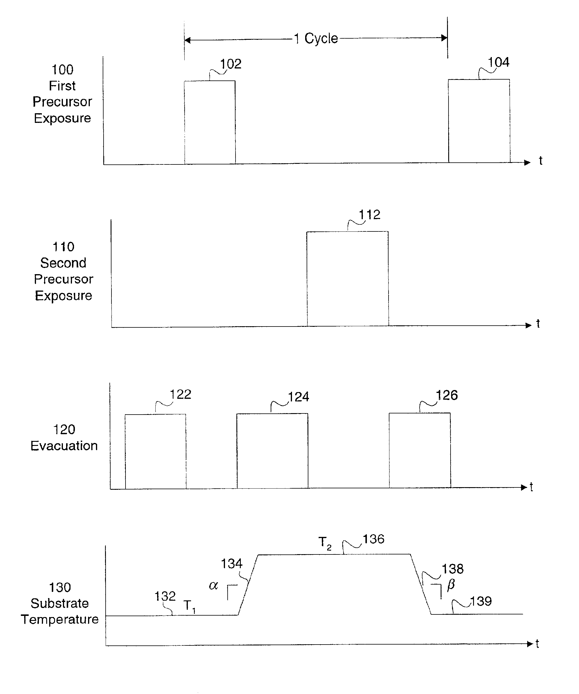
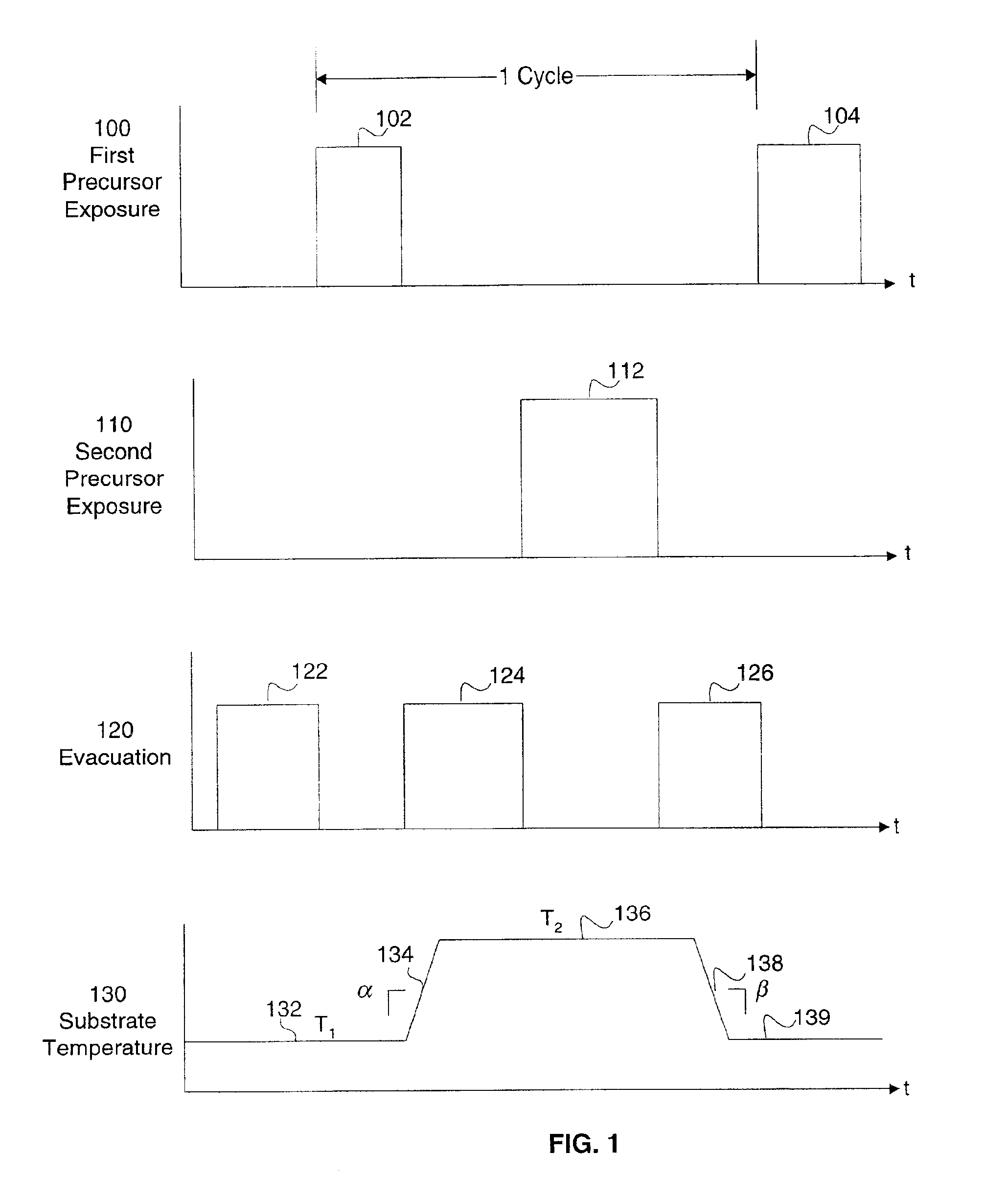
Method and apparatus for improved temperature control in atomic layer deposition
PatentInactiveUS6878402B2
Innovation
- The method involves decoupling the adsorption and reaction temperatures in ALD by adjusting the substrate temperature to different states, allowing the first reactant to adsorb at a lower temperature and react with the second reactant at a higher temperature, with rapid switching between these states using advanced heating and cooling techniques such as rapid thermal processing and laser irradiation, to enhance film purity and deposition rate.
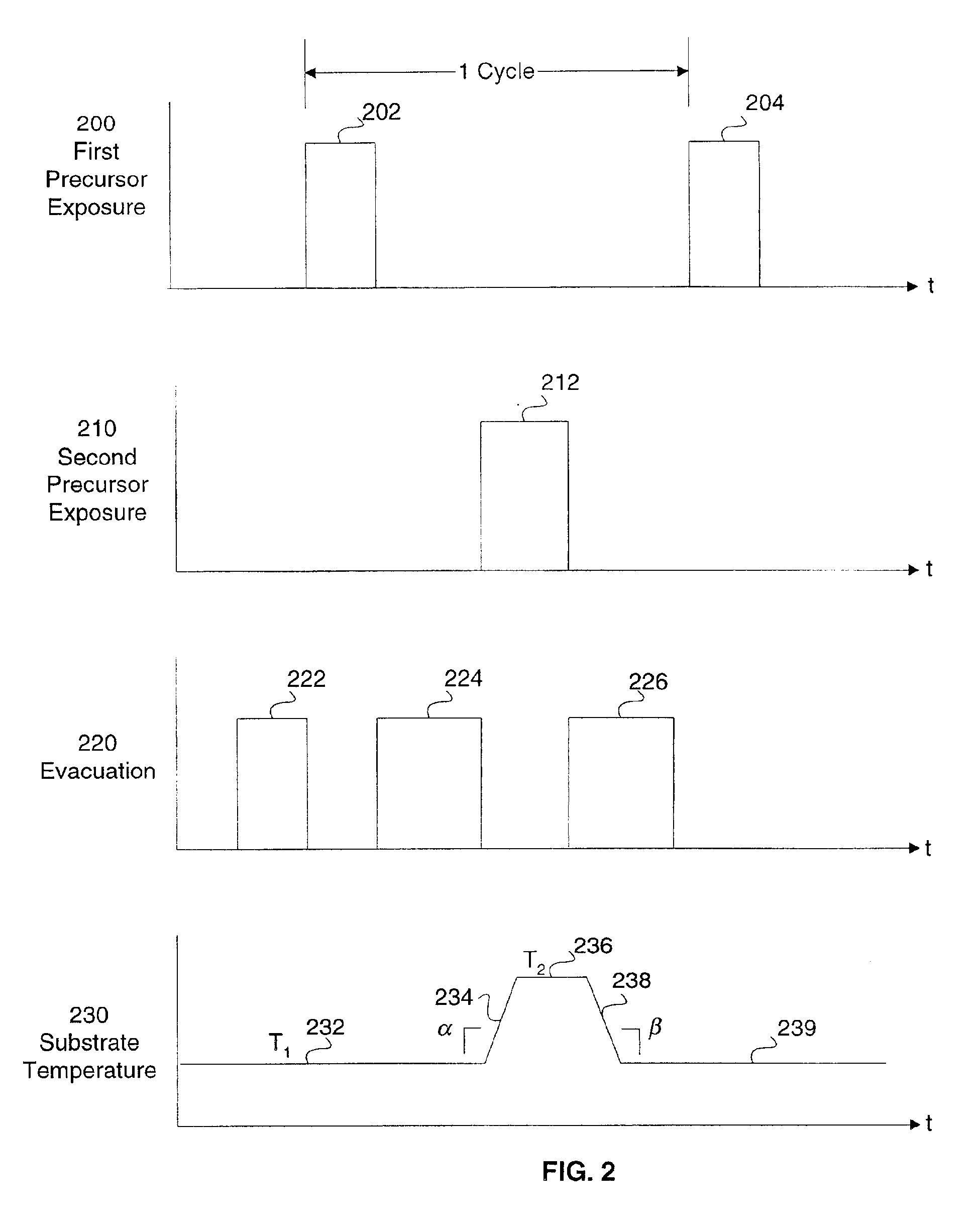

Controlling the Temperature of a Substrate in a Film Deposition Apparatus
PatentInactiveUS20070184189A1
Innovation
- The method involves decoupling the adsorption and reaction temperatures in ALD by adjusting the substrate temperature to two distinct states, allowing the first reactant to adsorb at a lower temperature and react with the second reactant at a higher temperature, with rapid switching between these states to enhance film purity and deposition rate, using techniques such as rapid thermal processing and laser irradiation for energy delivery.


Process Integration Challenges in Semiconductor Manufacturing
The integration of Atomic Layer Deposition (ALD) and Plasma Enhanced Chemical Vapor Deposition (PECVD) processes into semiconductor manufacturing workflows presents multifaceted challenges that significantly impact production efficiency and yield optimization. These challenges stem from the fundamental differences in process requirements, thermal budgets, and material compatibility between the two deposition techniques.
Thermal budget management represents one of the most critical integration challenges. ALD processes typically operate at lower temperatures ranging from 150°C to 400°C, while PECVD can function across a broader temperature spectrum from room temperature to 600°C. This temperature differential creates complex thermal cycling requirements that can induce mechanical stress in multilayer structures and affect the integrity of previously deposited films.
Sequential process compatibility poses another significant hurdle. The transition between ALD and PECVD steps requires careful consideration of chamber conditioning, residual gas management, and surface preparation protocols. Cross-contamination between processes can occur through precursor residues, plasma-induced surface modifications, or inadequate purging sequences, leading to interface defects and compromised film properties.
Equipment utilization and throughput optimization present ongoing challenges in high-volume manufacturing environments. ALD's inherently slower deposition rates compared to PECVD create bottlenecks in production lines designed for rapid processing. The integration requires sophisticated scheduling algorithms and potentially dedicated tool sets to maintain overall manufacturing efficiency while preserving process quality.
Interface engineering between ALD and PECVD layers demands precise control over surface chemistry and nucleation behavior. The atomic-scale precision of ALD can be compromised by plasma-induced damage from subsequent PECVD steps, while PECVD surfaces may not provide optimal nucleation sites for ALD processes. These interface challenges directly impact device performance parameters such as leakage current, breakdown voltage, and reliability metrics.
Process monitoring and metrology integration across both techniques requires advanced characterization capabilities. Real-time monitoring systems must accommodate the different process signatures and time scales of ALD and PECVD, necessitating sophisticated sensor integration and data correlation algorithms to ensure consistent process control and early defect detection throughout the integrated manufacturing sequence.
Quality Control Standards for Temperature-Dependent Films
Quality control standards for temperature-dependent films deposited via Atomic Layer Deposition (ALD) and Plasma Enhanced Chemical Vapor Deposition (PECVD) require comprehensive frameworks that address the unique thermal sensitivities inherent to each process. These standards must encompass measurement protocols, acceptance criteria, and validation procedures specifically tailored to temperature-sensitive film properties.
Film thickness uniformity represents a critical quality parameter, with ALD typically achieving superior conformality due to its self-limiting surface reactions. Standard measurement protocols employ spectroscopic ellipsometry and X-ray reflectometry with temperature-controlled sample stages to ensure consistent measurement conditions. Acceptance criteria typically specify thickness variations below 2% for ALD films and 5% for PECVD films across substrate surfaces.
Compositional analysis standards mandate energy-dispersive X-ray spectroscopy and X-ray photoelectron spectroscopy measurements at standardized temperatures to account for thermal drift effects. Temperature-dependent stoichiometry variations require documentation across the operational temperature range, with particular attention to hydrogen content in PECVD films and impurity incorporation in low-temperature ALD processes.
Mechanical property evaluation protocols address temperature-induced stress variations through wafer curvature measurements and nanoindentation testing. Standards specify stress measurement temperatures that correlate with intended application environments, recognizing that PECVD films often exhibit higher intrinsic stress due to ion bombardment effects compared to gentler ALD processes.
Electrical characterization standards encompass temperature-dependent resistivity, dielectric constant, and breakdown voltage measurements. These protocols account for the different defect densities and interface qualities achieved by each deposition method, with ALD generally producing superior electrical properties due to atomic-scale control.
Thermal stability assessment requires accelerated aging tests at elevated temperatures to evaluate film degradation mechanisms. Standards define exposure conditions, measurement intervals, and failure criteria specific to each deposition technique, acknowledging that PECVD films may exhibit different thermal evolution pathways compared to ALD films due to their distinct microstructures and bonding configurations.
Unlock deeper insights with PatSnap Eureka Quick Research — get a full tech report to explore trends and direct your research. Try now!
Generate Your Research Report Instantly with AI Agent
Supercharge your innovation with PatSnap Eureka AI Agent Platform!