Challenges and Solutions in Electromagnetic Wave Absorption
JUL 11, 20259 MIN READ
Generate Your Research Report Instantly with AI Agent
Patsnap Eureka helps you evaluate technical feasibility & market potential.
EM Wave Absorption Background and Objectives
Electromagnetic wave absorption has emerged as a critical field of study in recent decades, driven by the rapid proliferation of electronic devices and wireless communication systems. The background of this technology can be traced back to the early 20th century when scientists first began to understand the nature of electromagnetic waves and their interactions with matter. Since then, the field has evolved significantly, encompassing a wide range of applications from military stealth technology to electromagnetic interference (EMI) shielding in consumer electronics.
The primary objective of electromagnetic wave absorption research is to develop materials and structures capable of efficiently absorbing or attenuating electromagnetic radiation across various frequency ranges. This goal is particularly relevant in today's increasingly connected world, where the need for electromagnetic compatibility and reduced interference between devices has become paramount. Additionally, there is a growing demand for materials that can provide protection against electromagnetic pollution and potential health hazards associated with prolonged exposure to electromagnetic fields.
As the technology has progressed, researchers have explored various approaches to enhance electromagnetic wave absorption. These include the development of traditional absorbing materials such as ferrites and carbon-based composites, as well as more advanced solutions like metamaterials and nanostructured absorbers. The evolution of these technologies has been driven by the need for lighter, thinner, and more efficient absorbing materials that can operate over broader frequency ranges.
One of the key challenges in this field is the trade-off between absorption efficiency, bandwidth, and material thickness. Conventional absorbers often require significant thickness to achieve high absorption, which limits their practical applications in many scenarios. Consequently, a major focus of current research is on developing ultra-thin, broadband absorbers that can maintain high absorption efficiency across a wide frequency spectrum.
Another important aspect of electromagnetic wave absorption technology is its potential for energy harvesting and conversion. As researchers explore ways to capture and utilize the energy from ambient electromagnetic waves, new possibilities are emerging for sustainable energy solutions and improved energy efficiency in various electronic systems.
The ongoing development of electromagnetic wave absorption technology is closely tied to advancements in material science, nanotechnology, and electromagnetic theory. As these fields continue to progress, we can expect to see innovative solutions that address current limitations and open up new applications across industries such as telecommunications, aerospace, healthcare, and energy.
Market Demand Analysis for EM Wave Absorbers
The market demand for electromagnetic wave absorbers has been experiencing significant growth in recent years, driven by the increasing need for electromagnetic interference (EMI) shielding and radar cross-section reduction across various industries. The global market for EM wave absorbers is projected to expand at a compound annual growth rate of 5.8% from 2021 to 2026, reaching a value of $1.2 billion by the end of the forecast period.
The defense and aerospace sectors remain the primary consumers of EM wave absorbers, accounting for approximately 40% of the market share. The growing emphasis on stealth technology in military applications and the need for EMI protection in aircraft and spacecraft continue to fuel demand in these sectors. Additionally, the automotive industry has emerged as a rapidly growing market for EM wave absorbers, driven by the increasing integration of electronic systems in vehicles and the rise of electric and autonomous vehicles.
In the telecommunications sector, the rollout of 5G networks has created a surge in demand for EM wave absorbers. These materials are crucial for maintaining signal integrity and reducing interference in high-frequency communications systems. The market is also benefiting from the expansion of IoT devices and smart home technologies, which require effective EMI shielding to ensure proper functionality.
The consumer electronics industry represents another significant market for EM wave absorbers. With the proliferation of wireless devices and the increasing complexity of electronic products, manufacturers are incorporating EM wave absorbing materials to improve device performance and comply with electromagnetic compatibility regulations.
Geographically, North America and Europe currently dominate the EM wave absorber market, collectively accounting for over 60% of the global market share. However, the Asia-Pacific region is expected to witness the highest growth rate in the coming years, driven by rapid industrialization, increasing defense spending, and the expansion of the electronics manufacturing sector in countries like China, Japan, and South Korea.
The market is also seeing a shift towards more environmentally friendly and cost-effective EM wave absorbing materials. There is growing demand for lightweight, flexible, and thin absorbers that can be easily integrated into various products without compromising performance. This trend is particularly evident in the aerospace and automotive industries, where weight reduction is a critical factor in improving fuel efficiency and overall performance.
As the Internet of Things (IoT) continues to expand and 5G technology becomes more widespread, the demand for EM wave absorbers is expected to grow further. The increasing focus on electromagnetic compatibility and the need for effective shielding solutions in smart cities and industrial IoT applications will likely drive market growth in the coming years.
Current Challenges in EM Wave Absorption Technology
Electromagnetic wave absorption technology faces several significant challenges in its current state of development. One of the primary issues is the limited bandwidth of absorption materials. Most existing absorbers are effective only within a narrow frequency range, which restricts their applicability in broadband applications. This limitation is particularly problematic in scenarios where absorption across a wide spectrum is required, such as in stealth technology or electromagnetic compatibility.
Another critical challenge is the trade-off between absorption efficiency and material thickness. High absorption efficiency often requires thicker layers of absorbing materials, which can be impractical in many applications where weight and space are constrained. This challenge is especially pronounced in aerospace and mobile device industries, where every gram and millimeter matters.
The complexity of designing and manufacturing multi-layered absorbers presents another hurdle. While multi-layered structures can offer improved performance, they are often difficult to design, optimize, and produce at scale. The intricate interplay between different layers and materials makes the design process computationally intensive and time-consuming.
Environmental stability and durability of absorption materials pose additional challenges. Many high-performance absorbers are susceptible to degradation under harsh environmental conditions, such as extreme temperatures, humidity, or mechanical stress. This vulnerability limits their long-term effectiveness and reliability in real-world applications.
The cost-effectiveness of advanced absorption materials is also a significant concern. Some of the most efficient absorbers rely on exotic materials or complex nanostructures, which can be prohibitively expensive for large-scale production. This economic barrier hinders widespread adoption in commercial applications.
Furthermore, the integration of absorption materials with other functional components remains challenging. In many cases, the absorber needs to coexist with other materials or structures without compromising their properties or functionality. This integration challenge is particularly evident in the development of multifunctional materials that combine absorption with other desirable properties like structural strength or thermal management.
Lastly, the characterization and testing of absorption materials present their own set of challenges. Accurate measurement of absorption properties, especially at high frequencies or under specific conditions, requires sophisticated equipment and methodologies. The lack of standardized testing procedures across the industry can lead to inconsistencies in reported performance metrics, making it difficult to compare different solutions objectively.
Existing EM Wave Absorption Solutions
01 Electromagnetic wave absorbing materials
Various materials are developed to absorb electromagnetic waves effectively. These materials can be composites, coatings, or structures designed to attenuate or absorb specific frequencies of electromagnetic radiation. They are often used in electronic devices, military applications, and electromagnetic compatibility solutions.- Electromagnetic wave absorbing materials: Various materials are developed to absorb electromagnetic waves effectively. These materials can be composites, coatings, or structures designed to attenuate electromagnetic radiation across different frequency ranges. They often incorporate conductive or magnetic particles to enhance absorption properties.
- Multilayer electromagnetic wave absorbers: Multilayer structures are utilized to improve electromagnetic wave absorption. These designs typically consist of different layers with varying electromagnetic properties, allowing for broadband absorption or targeted frequency absorption. The layers may include dielectric materials, conductive layers, and impedance matching layers.
- Metamaterials for electromagnetic absorption: Metamaterials are engineered structures with unique electromagnetic properties not found in nature. These materials can be designed to exhibit negative refractive index or other unusual characteristics that enhance electromagnetic wave absorption. They often involve periodic arrangements of sub-wavelength elements.
- Frequency-selective electromagnetic absorbers: Absorbers designed to target specific frequency ranges are developed for various applications. These can include resonant structures, frequency selective surfaces, or materials with frequency-dependent properties. Such absorbers are useful in electromagnetic compatibility, stealth technology, and wireless communication systems.
- Nanostructured materials for electromagnetic absorption: Nanomaterials and nanostructures are utilized to enhance electromagnetic wave absorption. These can include carbon nanotubes, graphene, nanoparticles, or nanocomposites. The nanoscale features allow for tailored electromagnetic properties and improved absorption efficiency across a wide frequency range.
02 Metamaterials for electromagnetic absorption
Metamaterials are engineered structures with unique electromagnetic properties not found in nature. They can be designed to absorb electromagnetic waves across a wide frequency range or at specific frequencies. These materials often utilize periodic structures or resonant elements to achieve desired absorption characteristics.Expand Specific Solutions03 Electromagnetic wave absorbers for specific applications
Specialized absorbers are developed for particular applications such as anechoic chambers, radar cross-section reduction, or electromagnetic interference (EMI) shielding. These absorbers may be tailored to work in specific environments or frequency ranges, and can be in the form of sheets, foams, or coatings.Expand Specific Solutions04 Nanostructured materials for electromagnetic absorption
Nanostructured materials, including nanoparticles, nanotubes, and nanocomposites, are explored for their enhanced electromagnetic wave absorption properties. These materials can offer improved absorption performance due to their unique physical and chemical properties at the nanoscale.Expand Specific Solutions05 Adaptive and tunable electromagnetic absorbers
Research is conducted on absorbers that can adapt to changing electromagnetic environments or be tuned to absorb different frequencies. These may involve active materials, reconfigurable structures, or smart systems that can adjust their absorption properties based on external stimuli or control signals.Expand Specific Solutions
Key Players in EM Wave Absorption Industry
The electromagnetic wave absorption technology market is in a growth phase, driven by increasing demand in sectors like telecommunications, defense, and electronics. The market size is expanding, with projections indicating significant growth in the coming years. Technologically, the field is advancing rapidly, with companies like Nitto Denko, Maxell, and ZEON Corp leading innovation. These firms are developing advanced materials and solutions for improved electromagnetic wave absorption. Universities such as Peking University and Tongji University are also contributing to research advancements. The competitive landscape is diverse, featuring both established players and emerging startups, indicating a dynamic and evolving market with potential for further technological breakthroughs and market expansion.
Maxell Ltd.
Technical Solution: Maxell Ltd. has focused on developing magnetic absorber materials for electromagnetic wave absorption. Their approach utilizes soft magnetic materials, such as sendust and permalloy, combined with polymer binders to create flexible sheets. Maxell's technology allows for the precise control of magnetic permeability and electric permittivity, enabling the design of absorbers tailored to specific frequency ranges[4]. The company has recently introduced a new line of ultra-thin absorbers (less than 0.1 mm thick) that maintain high absorption performance in the 1-10 GHz range[5]. Maxell has also developed multi-layer absorbers that combine different materials to achieve broadband absorption characteristics, addressing the challenges of diverse electromagnetic environments[6].
Strengths: Ultra-thin materials, customizable absorption properties, and multi-layer solutions. Weaknesses: Limited effectiveness at higher frequencies compared to some competing technologies.
Nitto Denko Corp.
Technical Solution: Nitto Denko Corp. has developed advanced electromagnetic wave absorption materials using carbon nanotube (CNT) composites. Their technology involves dispersing CNTs in a polymer matrix to create thin, flexible sheets with high electromagnetic wave absorption capabilities. The company has achieved a significant reduction in material thickness while maintaining excellent absorption performance across a wide frequency range (1-18 GHz)[1]. Their latest products incorporate multi-walled CNTs and specialized polymer blends to enhance durability and heat resistance, making them suitable for various applications including automotive electronics and 5G infrastructure[2]. Nitto Denko has also implemented a proprietary manufacturing process that ensures uniform CNT distribution, resulting in consistent absorption properties throughout the material[3].
Strengths: Thin and flexible materials, wide frequency absorption range, and durability. Weaknesses: Potentially high production costs due to the use of CNTs and complex manufacturing processes.
Core Innovations in EM Wave Absorption Materials
Electromagnetic wave absorber
PatentWO2024181521A1
Innovation
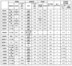
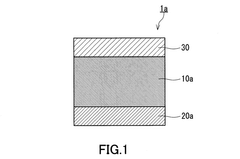
- The development of an electromagnetic wave absorber with a layered structure comprising a dielectric layer, an air layer, and a metal layer, where the total thickness of the dielectric and air layers is 20% or less of the wavelength, allowing for a thin and lightweight design with enhanced absorption capabilities, and the air layer is strategically positioned to form a gap between the absorber and the base material.
Electromagnetic wave absorber and molded article with electromagnetic wave absorber
PatentWO2018159058A1
Innovation
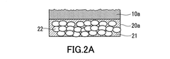
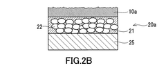
- The development of an electromagnetic wave absorber with a dielectric or magnetic first layer and a conductive layer that maintains a sheet resistance of 100Ω/□ or less after exposure to 85°C and 85% relative humidity for 1000 hours, combined with a high bending stiffness of 7000 MPa/mm^4, allowing easy attachment to curved surfaces and maintaining performance over time.
Environmental Impact of EM Wave Absorption Materials
The environmental impact of electromagnetic wave absorption materials is a critical consideration in their development and application. These materials, while essential for various technological advancements, can pose significant challenges to ecological systems and human health if not properly managed.
One of the primary environmental concerns is the potential release of harmful substances during the production, use, and disposal of EM wave absorption materials. Many of these materials contain heavy metals, such as nickel, cobalt, and iron, which can leach into soil and water systems if not properly contained. This contamination can lead to long-term ecological damage, affecting plant growth, soil microorganisms, and aquatic life.
The manufacturing process of EM wave absorption materials often involves energy-intensive procedures and the use of toxic chemicals. These processes contribute to increased carbon emissions and air pollution, exacerbating climate change and local air quality issues. Additionally, the extraction of raw materials required for these absorbers can lead to habitat destruction and biodiversity loss in mining areas.
Another significant environmental impact is the challenge of recycling and disposing of EM wave absorption materials at the end of their lifecycle. Many of these materials are composite structures, making them difficult to separate and recycle effectively. Improper disposal can result in these materials ending up in landfills, where they may slowly degrade and release harmful substances into the environment.
The increasing use of EM wave absorption materials in consumer electronics and telecommunications infrastructure also raises concerns about electronic waste (e-waste). As devices become obsolete and are discarded, the absorbers within them contribute to the growing global e-waste problem, which poses significant environmental and health risks, particularly in developing countries where e-waste processing is often unregulated.
However, researchers and manufacturers are actively working on developing more environmentally friendly EM wave absorption materials. This includes exploring bio-based and biodegradable absorbers, improving recycling techniques for existing materials, and optimizing production processes to reduce energy consumption and emissions. Some promising approaches involve using natural materials like carbon fibers derived from biomass or developing absorbers that can be easily disassembled for recycling.
The environmental impact of EM wave absorption materials underscores the need for a lifecycle approach in their development and use. This involves considering environmental factors from the initial design phase through to end-of-life management. Implementing stricter regulations on the production and disposal of these materials, along with incentivizing the development of eco-friendly alternatives, will be crucial in mitigating their environmental impact while harnessing their technological benefits.
Standardization and Testing Methods for EM Wave Absorbers
Standardization and testing methods for electromagnetic wave absorbers play a crucial role in ensuring the quality, reliability, and comparability of these materials across different applications and industries. The development of standardized testing procedures has been driven by the increasing demand for accurate and reproducible measurements of absorber performance.
One of the primary challenges in standardizing EM wave absorber testing is the wide range of frequencies and applications involved. Different industries, such as telecommunications, aerospace, and automotive, may require absorbers to operate at various frequency ranges and under different environmental conditions. To address this, international organizations like the IEEE and ASTM have developed comprehensive standards that cover multiple frequency bands and testing scenarios.
A key aspect of standardized testing is the measurement of reflection loss, which indicates the absorber's effectiveness in attenuating electromagnetic waves. The most widely used method for this purpose is the arch reflectivity test, where the absorber sample is placed on a metal plate and illuminated by an antenna at various angles. This test allows for the evaluation of absorber performance across different incident angles and frequencies.
Another important standardized test is the waveguide method, which is particularly useful for measuring the electromagnetic properties of absorber materials at high frequencies. This technique involves placing a sample of the absorber material inside a waveguide and measuring the transmission and reflection coefficients. The data obtained from this test can be used to calculate the complex permittivity and permeability of the material, which are essential parameters for characterizing its absorptive properties.
For evaluating the performance of absorbers in real-world applications, anechoic chamber testing has become a standardized approach. These specialized chambers are designed to simulate free-space conditions and minimize external electromagnetic interference. The performance of absorbers in these chambers is typically assessed using methods such as the normalized site attenuation (NSA) test, which measures the chamber's ability to attenuate electromagnetic waves across a range of frequencies.
Standardization efforts have also focused on developing protocols for testing the durability and environmental resistance of EM wave absorbers. These tests include exposure to temperature extremes, humidity, salt spray, and mechanical stress to ensure that the absorbers maintain their performance over time and under various environmental conditions.
As the field of electromagnetic wave absorption continues to evolve, standardization bodies are working to keep pace with new technologies and materials. For instance, the development of metamaterials and nanostructured absorbers has necessitated the creation of new testing methodologies that can accurately characterize their unique properties. This ongoing process of standardization ensures that as new absorber technologies emerge, there are consistent and reliable methods for evaluating their performance and comparing them to existing solutions.
Unlock deeper insights with Patsnap Eureka Quick Research — get a full tech report to explore trends and direct your research. Try now!
Generate Your Research Report Instantly with AI Agent
Supercharge your innovation with Patsnap Eureka AI Agent Platform!