
Compare HBM Memory Clock Speeds for Peak Performance Metrics
MAY 18, 20268 MIN READ
Generate Your Research Report Instantly with AI Agent
Patsnap Eureka helps you evaluate technical feasibility & market potential.
HBM Memory Evolution and Performance Goals
High Bandwidth Memory (HBM) technology emerged from the critical need to address the growing memory bandwidth bottleneck in high-performance computing applications. The evolution began in the early 2010s when traditional DDR memory architectures could no longer satisfy the exponential data throughput demands of graphics processing units, artificial intelligence accelerators, and high-performance computing systems.
The foundational development of HBM represented a paradigm shift from conventional memory design philosophies. Unlike traditional memory modules that relied on increasing clock frequencies to achieve higher bandwidth, HBM introduced a revolutionary approach utilizing through-silicon via (TSV) technology and 3D stacking architectures. This innovation enabled significantly wider memory interfaces while maintaining relatively conservative clock speeds, fundamentally changing the performance optimization equation.
The primary technical objective driving HBM development centers on achieving maximum memory bandwidth density while minimizing power consumption and physical footprint. Early HBM generations targeted bandwidth capabilities exceeding 128 GB/s per stack, representing a substantial improvement over conventional GDDR5 memory systems. The architecture's inherent design allows for multiple memory dies to be vertically integrated, creating a compact yet highly efficient memory subsystem.
Performance goals have continuously evolved across HBM generations, with each iteration pushing the boundaries of achievable bandwidth and capacity. HBM2 established targets of 256 GB/s per stack, while HBM2E extended these objectives to 460 GB/s. The latest HBM3 specifications aim for bandwidth exceeding 665 GB/s per stack, demonstrating the technology's aggressive performance trajectory.
The strategic importance of optimizing HBM clock speeds lies in balancing multiple competing factors including signal integrity, power efficiency, and thermal management. Unlike conventional memory where higher clock frequencies directly correlate with improved performance, HBM's wide interface architecture enables peak performance through optimized clock speed selection rather than maximum frequency operation.
Contemporary performance objectives emphasize not only raw bandwidth achievements but also latency optimization and energy efficiency metrics. The technology roadmap indicates continued focus on achieving higher effective bandwidth through improved clock speed management, advanced error correction capabilities, and enhanced signal processing techniques that collectively contribute to superior system-level performance characteristics.
The foundational development of HBM represented a paradigm shift from conventional memory design philosophies. Unlike traditional memory modules that relied on increasing clock frequencies to achieve higher bandwidth, HBM introduced a revolutionary approach utilizing through-silicon via (TSV) technology and 3D stacking architectures. This innovation enabled significantly wider memory interfaces while maintaining relatively conservative clock speeds, fundamentally changing the performance optimization equation.
The primary technical objective driving HBM development centers on achieving maximum memory bandwidth density while minimizing power consumption and physical footprint. Early HBM generations targeted bandwidth capabilities exceeding 128 GB/s per stack, representing a substantial improvement over conventional GDDR5 memory systems. The architecture's inherent design allows for multiple memory dies to be vertically integrated, creating a compact yet highly efficient memory subsystem.
Performance goals have continuously evolved across HBM generations, with each iteration pushing the boundaries of achievable bandwidth and capacity. HBM2 established targets of 256 GB/s per stack, while HBM2E extended these objectives to 460 GB/s. The latest HBM3 specifications aim for bandwidth exceeding 665 GB/s per stack, demonstrating the technology's aggressive performance trajectory.
The strategic importance of optimizing HBM clock speeds lies in balancing multiple competing factors including signal integrity, power efficiency, and thermal management. Unlike conventional memory where higher clock frequencies directly correlate with improved performance, HBM's wide interface architecture enables peak performance through optimized clock speed selection rather than maximum frequency operation.
Contemporary performance objectives emphasize not only raw bandwidth achievements but also latency optimization and energy efficiency metrics. The technology roadmap indicates continued focus on achieving higher effective bandwidth through improved clock speed management, advanced error correction capabilities, and enhanced signal processing techniques that collectively contribute to superior system-level performance characteristics.
Market Demand for High-Bandwidth Memory Solutions
The global high-bandwidth memory market is experiencing unprecedented growth driven by the exponential increase in data-intensive applications across multiple sectors. Artificial intelligence and machine learning workloads have emerged as primary catalysts, demanding memory solutions that can deliver sustained high throughput with minimal latency. Graphics processing units, particularly those designed for AI training and inference, require memory subsystems capable of feeding massive parallel processing arrays with continuous data streams.
Data center infrastructure modernization represents another significant demand driver, as cloud service providers seek to optimize performance per watt metrics while handling increasingly complex computational workloads. The proliferation of high-performance computing applications in scientific research, financial modeling, and simulation environments has created sustained demand for memory technologies that can eliminate bottlenecks in data-intensive operations.
Gaming and professional graphics markets continue to push bandwidth requirements higher, with next-generation gaming engines and real-time ray tracing applications demanding unprecedented memory performance. The emergence of virtual and augmented reality platforms has further intensified these requirements, as immersive experiences require seamless data delivery to maintain user engagement and prevent motion sickness.
Automotive sector transformation toward autonomous driving systems has opened new market segments for high-bandwidth memory solutions. Advanced driver assistance systems and autonomous vehicle platforms require real-time processing of sensor data from multiple sources, creating demand for memory architectures that can support parallel data streams with deterministic latency characteristics.
Edge computing deployment across telecommunications infrastructure, particularly with 5G network rollouts, has generated additional market opportunities. Network function virtualization and software-defined networking implementations require memory solutions that can handle packet processing at line rates while maintaining low power consumption profiles suitable for distributed deployment scenarios.
The convergence of these market forces has created a robust ecosystem where memory clock speed optimization directly translates to competitive advantages across multiple application domains, establishing high-bandwidth memory as a critical enabling technology for next-generation computing platforms.
Data center infrastructure modernization represents another significant demand driver, as cloud service providers seek to optimize performance per watt metrics while handling increasingly complex computational workloads. The proliferation of high-performance computing applications in scientific research, financial modeling, and simulation environments has created sustained demand for memory technologies that can eliminate bottlenecks in data-intensive operations.
Gaming and professional graphics markets continue to push bandwidth requirements higher, with next-generation gaming engines and real-time ray tracing applications demanding unprecedented memory performance. The emergence of virtual and augmented reality platforms has further intensified these requirements, as immersive experiences require seamless data delivery to maintain user engagement and prevent motion sickness.
Automotive sector transformation toward autonomous driving systems has opened new market segments for high-bandwidth memory solutions. Advanced driver assistance systems and autonomous vehicle platforms require real-time processing of sensor data from multiple sources, creating demand for memory architectures that can support parallel data streams with deterministic latency characteristics.
Edge computing deployment across telecommunications infrastructure, particularly with 5G network rollouts, has generated additional market opportunities. Network function virtualization and software-defined networking implementations require memory solutions that can handle packet processing at line rates while maintaining low power consumption profiles suitable for distributed deployment scenarios.
The convergence of these market forces has created a robust ecosystem where memory clock speed optimization directly translates to competitive advantages across multiple application domains, establishing high-bandwidth memory as a critical enabling technology for next-generation computing platforms.
Current HBM Clock Speed Limitations and Challenges
HBM technology faces several fundamental limitations that constrain clock speed optimization and peak performance achievement. The primary bottleneck stems from thermal management challenges, as higher clock frequencies generate exponential heat increases within the vertically stacked memory dies. Current HBM implementations typically operate between 1.6-3.2 GHz, with thermal dissipation becoming critically problematic beyond these thresholds.
Power consumption represents another significant constraint affecting clock speed scalability. Each increment in memory clock frequency demands substantially higher power delivery, creating a cascading effect on system-level power budgets. Modern HBM modules already consume 15-25 watts under standard operating conditions, and aggressive clock speed increases can push consumption beyond acceptable limits for mobile and data center applications.
Signal integrity degradation emerges as clock speeds approach physical limitations of the Through-Silicon-Via (TSV) interconnect technology. High-frequency signals experience increased crosstalk, electromagnetic interference, and timing skew across the vertical memory stack. These phenomena directly impact data reliability and force manufacturers to implement conservative timing margins that ultimately limit achievable performance gains.
Manufacturing process variations create additional challenges for consistent high-speed operation across production volumes. Die-to-die variations in electrical characteristics become more pronounced at elevated frequencies, resulting in yield reduction and increased production costs. Current fabrication technologies struggle to maintain uniform performance characteristics across all memory dies within a single HBM stack when operating at maximum clock speeds.
Voltage scaling limitations further constrain clock speed optimization efforts. While traditional memory technologies benefit from voltage increases to support higher frequencies, HBM's dense vertical architecture amplifies voltage-related reliability concerns. Electromigration effects and long-term reliability degradation become accelerated factors that manufacturers must carefully balance against performance requirements.
System-level integration challenges compound these technical limitations. Host processors and memory controllers must synchronize with HBM timing requirements, creating interdependencies that limit overall system optimization flexibility. Current controller architectures often cannot fully exploit theoretical HBM bandwidth capabilities due to protocol overhead and latency considerations that become more severe at higher clock frequencies.
Power consumption represents another significant constraint affecting clock speed scalability. Each increment in memory clock frequency demands substantially higher power delivery, creating a cascading effect on system-level power budgets. Modern HBM modules already consume 15-25 watts under standard operating conditions, and aggressive clock speed increases can push consumption beyond acceptable limits for mobile and data center applications.
Signal integrity degradation emerges as clock speeds approach physical limitations of the Through-Silicon-Via (TSV) interconnect technology. High-frequency signals experience increased crosstalk, electromagnetic interference, and timing skew across the vertical memory stack. These phenomena directly impact data reliability and force manufacturers to implement conservative timing margins that ultimately limit achievable performance gains.
Manufacturing process variations create additional challenges for consistent high-speed operation across production volumes. Die-to-die variations in electrical characteristics become more pronounced at elevated frequencies, resulting in yield reduction and increased production costs. Current fabrication technologies struggle to maintain uniform performance characteristics across all memory dies within a single HBM stack when operating at maximum clock speeds.
Voltage scaling limitations further constrain clock speed optimization efforts. While traditional memory technologies benefit from voltage increases to support higher frequencies, HBM's dense vertical architecture amplifies voltage-related reliability concerns. Electromigration effects and long-term reliability degradation become accelerated factors that manufacturers must carefully balance against performance requirements.
System-level integration challenges compound these technical limitations. Host processors and memory controllers must synchronize with HBM timing requirements, creating interdependencies that limit overall system optimization flexibility. Current controller architectures often cannot fully exploit theoretical HBM bandwidth capabilities due to protocol overhead and latency considerations that become more severe at higher clock frequencies.
Existing HBM Clock Speed Optimization Methods
01 Dynamic clock frequency adjustment for HBM memory
Methods and systems for dynamically adjusting the clock frequency of high bandwidth memory based on workload requirements, thermal conditions, and power constraints. These techniques allow for optimal performance scaling by increasing clock speeds during high-demand operations and reducing them during idle or low-activity periods to improve power efficiency.- Dynamic clock frequency adjustment for HBM memory: Methods and systems for dynamically adjusting the clock frequency of high bandwidth memory based on workload requirements, thermal conditions, and power constraints. These techniques enable optimal performance by scaling memory clock speeds in real-time according to system demands and operating conditions.
- Clock synchronization and timing control in HBM systems: Techniques for maintaining precise clock synchronization between memory controllers and high bandwidth memory modules. These methods ensure proper timing relationships and minimize clock skew to maintain data integrity and maximize memory performance across multiple memory stacks.
- Power management and clock gating for HBM memory: Power optimization strategies that involve selective clock gating and frequency scaling to reduce power consumption in high bandwidth memory systems. These approaches balance performance requirements with energy efficiency by controlling clock distribution and enabling low-power modes during idle periods.
- Clock generation and phase-locked loop circuits for HBM: Circuit designs and methodologies for generating stable, high-frequency clocks required for high bandwidth memory operation. These solutions include phase-locked loop implementations, clock multiplication techniques, and jitter reduction methods to ensure reliable memory timing at high speeds.
- Memory interface timing and clock domain crossing: Solutions for managing clock domain transitions and interface timing in high bandwidth memory systems. These techniques address challenges related to crossing between different clock domains, maintaining signal integrity, and ensuring proper setup and hold times for reliable data transfer.
02 Clock synchronization and timing control mechanisms
Techniques for maintaining precise clock synchronization between memory controllers and high bandwidth memory devices. These methods ensure proper timing relationships, reduce clock skew, and maintain signal integrity across multiple memory channels operating at high frequencies.Expand Specific Solutions03 Power management and thermal optimization for high-speed memory clocking
Systems and methods for managing power consumption and thermal characteristics when operating memory at elevated clock frequencies. These approaches include adaptive voltage scaling, thermal throttling mechanisms, and intelligent power gating to maintain system stability while maximizing performance.Expand Specific Solutions04 Memory interface and controller optimization for enhanced clock performance
Advanced memory controller architectures and interface designs that support higher clock speeds and improved data throughput. These solutions focus on optimizing the physical layer, reducing latency, and enhancing the overall memory subsystem performance through improved clocking schemes.Expand Specific Solutions05 Clock generation and distribution circuits for high bandwidth memory
Specialized clock generation and distribution circuits designed to provide stable, low-jitter clock signals to high bandwidth memory systems. These circuits incorporate phase-locked loops, delay-locked loops, and other timing circuits to ensure reliable operation at high frequencies while minimizing power consumption and electromagnetic interference.Expand Specific Solutions
Leading HBM Manufacturers and Industry Players
The HBM memory market is experiencing rapid growth driven by AI and high-performance computing demands, with the industry transitioning from early adoption to mainstream deployment across data centers and edge computing applications. Market size has expanded significantly as memory bandwidth requirements intensify, particularly for GPU-accelerated workloads and machine learning applications. Technology maturity varies considerably among key players, with Samsung Electronics and Micron Technology leading in manufacturing capabilities and production volumes, while Intel and NVIDIA drive integration and optimization efforts. Advanced Micro Devices and Google represent major consumers pushing performance boundaries, whereas emerging players like ChangXin Memory Technologies and AvicenaTech are developing next-generation interconnect solutions. The competitive landscape shows established memory manufacturers dominating current HBM3 implementations, while semiconductor giants and cloud providers are investing heavily in future HBM4 and beyond technologies to achieve peak performance metrics.
Samsung Electronics Co., Ltd.
Technical Solution: Samsung has developed HBM3E memory technology with clock speeds reaching up to 9.6 Gbps per pin, delivering peak bandwidth of 1.2 TB/s for high-performance computing applications. Their advanced manufacturing process utilizes through-silicon via (TSV) technology and optimized thermal management to maintain stable performance at these elevated clock frequencies. The company's HBM solutions feature enhanced error correction capabilities and power efficiency improvements, making them suitable for AI accelerators, graphics processors, and data center applications where memory bandwidth is critical for overall system performance.
Strengths: Leading manufacturing capabilities and proven track record in memory technology. Weaknesses: Higher cost compared to traditional memory solutions and complex integration requirements.
Micron Technology, Inc.
Technical Solution: Micron's HBM3 Gen2 memory achieves clock speeds of up to 8.4 Gbps with peak bandwidth exceeding 1.1 TB/s per stack. Their technology focuses on optimizing signal integrity through advanced packaging techniques and implementing adaptive voltage scaling to maintain performance across different operating conditions. Micron's HBM solutions incorporate proprietary thermal interface materials and innovative die stacking methodologies to ensure reliable operation at high frequencies while minimizing power consumption and heat generation in demanding computational workloads.
Strengths: Strong focus on power efficiency and thermal management solutions. Weaknesses: Slightly lower peak performance compared to some competitors and limited production capacity.
Core Patents in HBM Performance Enhancement
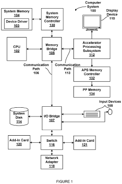
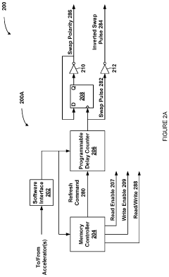
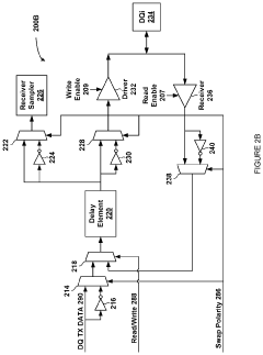
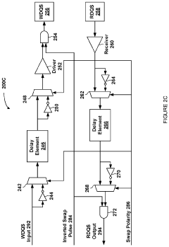
Mitigating duty cycle distortion degradation due to device aging on high-bandwidth memory interface
PatentActiveUS20230162780A1
Innovation
- A dynamic multiplexing circuit that switches between inverted and non-inverted data paths within the memory device's delay lines, using swap pulses with controllable delay and pulse width to mitigate asymmetric aging by changing polarity during refresh commands, thereby preventing prolonged exposure to sequences of zero or one values.
High speed memory interface
PatentActiveUS20190179791A1
Innovation
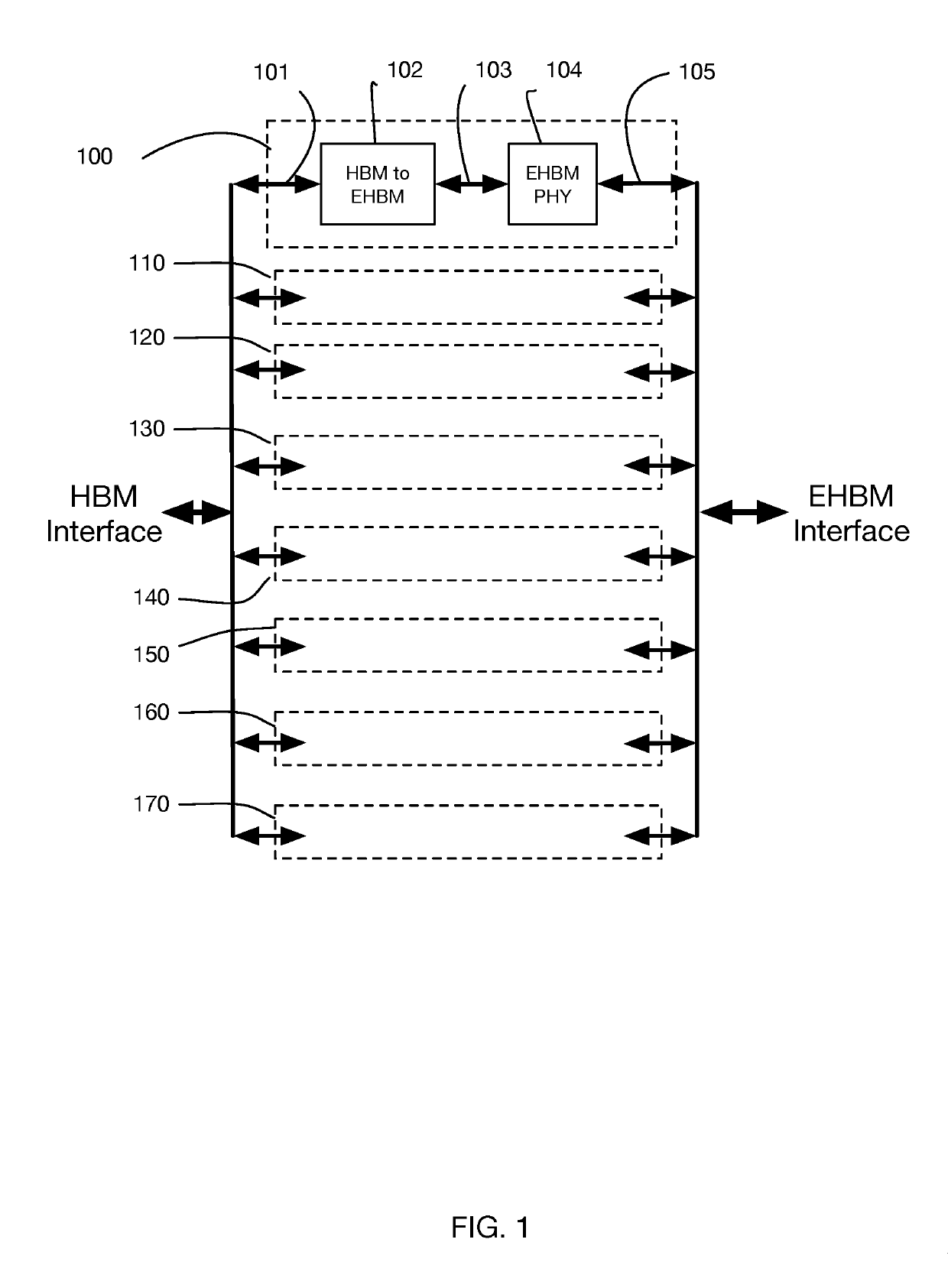
- The Enhanced HBM (EHBM) interface reduces the number of physical wires while operating at higher signaling rates, using a lower-cost organic interposer and fewer wires to maintain bandwidth, with each wire operating at a much higher signaling rate, and employs CNRZ-5 channels for efficient data transmission over six physical interconnection wires, along with clock signals, to achieve this.


HBM Performance Benchmarking Standards
The establishment of standardized HBM performance benchmarking protocols has become increasingly critical as memory subsystems evolve to support diverse computational workloads. Current benchmarking standards primarily focus on synthetic workloads that measure theoretical peak bandwidth and latency characteristics, yet these metrics often fail to capture real-world performance variations across different application domains.
Industry-standard benchmarking suites such as STREAM, SPEC CPU, and custom GPU compute benchmarks provide foundational metrics for HBM evaluation. However, these tools exhibit significant limitations when assessing clock speed impacts on actual system performance. The lack of standardized methodologies for correlating memory clock frequencies with application-specific performance outcomes creates substantial challenges for system architects and performance engineers.
Emerging benchmarking frameworks are incorporating more sophisticated workload characterization techniques that account for memory access patterns, data locality, and concurrent processing demands. These advanced methodologies enable more accurate assessment of how HBM clock speed variations translate into measurable performance improvements across different computational scenarios.
The development of cross-platform benchmarking standards remains fragmented, with different vendors implementing proprietary evaluation metrics that complicate direct performance comparisons. This fragmentation particularly affects enterprise procurement decisions where standardized performance baselines are essential for technology evaluation and selection processes.
Recent initiatives by industry consortiums aim to establish unified benchmarking protocols that incorporate both synthetic and real-world workload scenarios. These standards emphasize reproducible testing conditions, standardized reporting formats, and comprehensive coverage of memory subsystem characteristics including bandwidth utilization efficiency, power consumption metrics, and thermal performance under sustained workloads.
The integration of machine learning workloads into standard benchmarking suites represents a significant evolution in HBM performance evaluation methodologies. These workloads demonstrate distinct memory access patterns that reveal performance characteristics not captured by traditional computational benchmarks, providing more comprehensive insights into HBM clock speed optimization strategies for contemporary applications.
Industry-standard benchmarking suites such as STREAM, SPEC CPU, and custom GPU compute benchmarks provide foundational metrics for HBM evaluation. However, these tools exhibit significant limitations when assessing clock speed impacts on actual system performance. The lack of standardized methodologies for correlating memory clock frequencies with application-specific performance outcomes creates substantial challenges for system architects and performance engineers.
Emerging benchmarking frameworks are incorporating more sophisticated workload characterization techniques that account for memory access patterns, data locality, and concurrent processing demands. These advanced methodologies enable more accurate assessment of how HBM clock speed variations translate into measurable performance improvements across different computational scenarios.
The development of cross-platform benchmarking standards remains fragmented, with different vendors implementing proprietary evaluation metrics that complicate direct performance comparisons. This fragmentation particularly affects enterprise procurement decisions where standardized performance baselines are essential for technology evaluation and selection processes.
Recent initiatives by industry consortiums aim to establish unified benchmarking protocols that incorporate both synthetic and real-world workload scenarios. These standards emphasize reproducible testing conditions, standardized reporting formats, and comprehensive coverage of memory subsystem characteristics including bandwidth utilization efficiency, power consumption metrics, and thermal performance under sustained workloads.
The integration of machine learning workloads into standard benchmarking suites represents a significant evolution in HBM performance evaluation methodologies. These workloads demonstrate distinct memory access patterns that reveal performance characteristics not captured by traditional computational benchmarks, providing more comprehensive insights into HBM clock speed optimization strategies for contemporary applications.
Thermal Management in High-Speed HBM Systems
Thermal management represents one of the most critical engineering challenges in high-speed HBM systems, directly impacting the achievable memory clock speeds and overall performance metrics. As HBM memory operates at increasingly higher frequencies to meet performance demands, the power density within the memory stack escalates exponentially, creating substantial heat generation that must be effectively dissipated to maintain system stability and prevent performance throttling.
The relationship between memory clock speeds and thermal characteristics follows a non-linear progression, where each increment in operating frequency results in disproportionately higher heat output. This thermal behavior becomes particularly pronounced when comparing different HBM generations operating at their peak performance thresholds. HBM3 systems, for instance, generate significantly more heat per unit area compared to HBM2 when both operate at their respective maximum clock speeds, necessitating more sophisticated cooling solutions.
Advanced thermal management strategies have evolved to address these challenges through multiple approaches. Through-silicon via (TSV) technology plays a crucial role in heat dissipation by providing vertical thermal pathways within the memory stack. Additionally, micro-channel cooling systems and advanced thermal interface materials have become essential components for maintaining optimal operating temperatures during peak performance scenarios.
The thermal design considerations extend beyond simple heat removal to encompass thermal uniformity across the memory array. Temperature gradients within HBM stacks can lead to performance variations and reliability issues, making uniform thermal distribution as important as absolute temperature control. This requirement becomes increasingly complex as memory densities increase and operating frequencies push toward theoretical limits.
Emerging thermal management solutions include integrated heat spreaders, advanced packaging techniques, and dynamic thermal monitoring systems that can adjust performance parameters in real-time based on temperature feedback. These innovations enable HBM systems to sustain higher clock speeds for extended periods while maintaining thermal stability and ensuring long-term reliability across various operating conditions.
The relationship between memory clock speeds and thermal characteristics follows a non-linear progression, where each increment in operating frequency results in disproportionately higher heat output. This thermal behavior becomes particularly pronounced when comparing different HBM generations operating at their peak performance thresholds. HBM3 systems, for instance, generate significantly more heat per unit area compared to HBM2 when both operate at their respective maximum clock speeds, necessitating more sophisticated cooling solutions.
Advanced thermal management strategies have evolved to address these challenges through multiple approaches. Through-silicon via (TSV) technology plays a crucial role in heat dissipation by providing vertical thermal pathways within the memory stack. Additionally, micro-channel cooling systems and advanced thermal interface materials have become essential components for maintaining optimal operating temperatures during peak performance scenarios.
The thermal design considerations extend beyond simple heat removal to encompass thermal uniformity across the memory array. Temperature gradients within HBM stacks can lead to performance variations and reliability issues, making uniform thermal distribution as important as absolute temperature control. This requirement becomes increasingly complex as memory densities increase and operating frequencies push toward theoretical limits.
Emerging thermal management solutions include integrated heat spreaders, advanced packaging techniques, and dynamic thermal monitoring systems that can adjust performance parameters in real-time based on temperature feedback. These innovations enable HBM systems to sustain higher clock speeds for extended periods while maintaining thermal stability and ensuring long-term reliability across various operating conditions.
Unlock deeper insights with Patsnap Eureka Quick Research — get a full tech report to explore trends and direct your research. Try now!
Generate Your Research Report Instantly with AI Agent
Supercharge your innovation with Patsnap Eureka AI Agent Platform!