
Optimize HBM Memory Interconnect Design for Energy Savings
MAY 18, 20269 MIN READ
Generate Your Research Report Instantly with AI Agent
Patsnap Eureka helps you evaluate technical feasibility & market potential.
HBM Interconnect Energy Optimization Background and Goals
High Bandwidth Memory (HBM) technology has emerged as a critical component in modern computing systems, particularly in data-intensive applications such as artificial intelligence, high-performance computing, and graphics processing. The evolution of HBM from its initial introduction in 2013 to the current HBM3 generation demonstrates a consistent pursuit of higher bandwidth and capacity while maintaining compact form factors through advanced 3D stacking architectures.
The interconnect design within HBM modules represents a fundamental challenge in semiconductor engineering, as it must facilitate massive data throughput while operating within stringent power budgets. Traditional memory architectures face increasing limitations as data transfer rates scale exponentially, leading to proportional increases in power consumption that threaten system-level efficiency and thermal management capabilities.
Current HBM implementations utilize through-silicon vias (TSVs) and microbumps to create vertical interconnections between stacked memory dies, enabling unprecedented bandwidth density. However, these interconnect structures contribute significantly to overall power consumption through resistive losses, capacitive charging, and signal integrity maintenance requirements. The challenge intensifies as memory speeds approach multi-gigabit per second rates per channel.
The primary technical objective centers on developing innovative interconnect architectures that maintain or enhance data transfer performance while substantially reducing energy consumption per bit transferred. This involves optimizing signal encoding schemes, implementing advanced power management techniques, and exploring novel materials and manufacturing processes that minimize parasitic effects inherent in high-density vertical interconnections.
Secondary goals include improving thermal characteristics of interconnect structures, as reduced power consumption directly correlates with lower heat generation and improved system reliability. Additionally, the optimization must consider manufacturing scalability and cost-effectiveness to ensure commercial viability across diverse market segments.
The strategic importance of this optimization extends beyond individual memory modules to encompass entire system architectures, where memory power consumption often represents a significant portion of total system power budgets. Successful energy optimization in HBM interconnects could enable new classes of power-efficient computing systems and extend battery life in mobile high-performance applications.
The interconnect design within HBM modules represents a fundamental challenge in semiconductor engineering, as it must facilitate massive data throughput while operating within stringent power budgets. Traditional memory architectures face increasing limitations as data transfer rates scale exponentially, leading to proportional increases in power consumption that threaten system-level efficiency and thermal management capabilities.
Current HBM implementations utilize through-silicon vias (TSVs) and microbumps to create vertical interconnections between stacked memory dies, enabling unprecedented bandwidth density. However, these interconnect structures contribute significantly to overall power consumption through resistive losses, capacitive charging, and signal integrity maintenance requirements. The challenge intensifies as memory speeds approach multi-gigabit per second rates per channel.
The primary technical objective centers on developing innovative interconnect architectures that maintain or enhance data transfer performance while substantially reducing energy consumption per bit transferred. This involves optimizing signal encoding schemes, implementing advanced power management techniques, and exploring novel materials and manufacturing processes that minimize parasitic effects inherent in high-density vertical interconnections.
Secondary goals include improving thermal characteristics of interconnect structures, as reduced power consumption directly correlates with lower heat generation and improved system reliability. Additionally, the optimization must consider manufacturing scalability and cost-effectiveness to ensure commercial viability across diverse market segments.
The strategic importance of this optimization extends beyond individual memory modules to encompass entire system architectures, where memory power consumption often represents a significant portion of total system power budgets. Successful energy optimization in HBM interconnects could enable new classes of power-efficient computing systems and extend battery life in mobile high-performance applications.
Market Demand for Energy-Efficient HBM Solutions
The global semiconductor industry is experiencing unprecedented demand for high-bandwidth memory solutions, driven by the explosive growth of artificial intelligence, machine learning, and high-performance computing applications. Data centers worldwide are consuming increasingly massive amounts of energy, with memory subsystems accounting for a significant portion of total power consumption. This trend has created urgent market pressure for energy-efficient HBM solutions that can deliver superior performance while reducing operational costs and environmental impact.
Enterprise customers, particularly hyperscale data center operators and cloud service providers, are actively seeking memory technologies that can optimize their total cost of ownership. Energy efficiency has become a critical procurement criterion, as organizations face mounting pressure to meet sustainability targets and reduce carbon footprints. The demand extends beyond traditional performance metrics to encompass power consumption per bit transferred and thermal management capabilities.
The automotive sector represents an emerging high-growth market segment for energy-efficient HBM solutions. Advanced driver assistance systems, autonomous vehicles, and in-vehicle infotainment systems require substantial memory bandwidth while operating under strict power constraints. Battery-powered applications in this sector particularly value energy-optimized interconnect designs that can extend operational range and reduce cooling requirements.
Edge computing applications are driving demand for compact, power-efficient HBM solutions that can operate in resource-constrained environments. These deployments often lack sophisticated cooling infrastructure, making energy-efficient interconnect design essential for reliable operation. The proliferation of edge AI applications has intensified this market need.
Mobile and portable device manufacturers are increasingly incorporating HBM technology for graphics processing and AI acceleration. These applications demand ultra-low power consumption to preserve battery life while maintaining high performance levels. The consumer electronics market represents substantial volume potential for energy-optimized HBM solutions.
Regulatory pressures and environmental compliance requirements are further amplifying market demand. Government initiatives promoting energy efficiency in computing infrastructure are creating additional incentives for organizations to adopt power-optimized memory solutions. This regulatory landscape is expected to strengthen market demand for innovative HBM interconnect designs that prioritize energy savings without compromising performance capabilities.
Enterprise customers, particularly hyperscale data center operators and cloud service providers, are actively seeking memory technologies that can optimize their total cost of ownership. Energy efficiency has become a critical procurement criterion, as organizations face mounting pressure to meet sustainability targets and reduce carbon footprints. The demand extends beyond traditional performance metrics to encompass power consumption per bit transferred and thermal management capabilities.
The automotive sector represents an emerging high-growth market segment for energy-efficient HBM solutions. Advanced driver assistance systems, autonomous vehicles, and in-vehicle infotainment systems require substantial memory bandwidth while operating under strict power constraints. Battery-powered applications in this sector particularly value energy-optimized interconnect designs that can extend operational range and reduce cooling requirements.
Edge computing applications are driving demand for compact, power-efficient HBM solutions that can operate in resource-constrained environments. These deployments often lack sophisticated cooling infrastructure, making energy-efficient interconnect design essential for reliable operation. The proliferation of edge AI applications has intensified this market need.
Mobile and portable device manufacturers are increasingly incorporating HBM technology for graphics processing and AI acceleration. These applications demand ultra-low power consumption to preserve battery life while maintaining high performance levels. The consumer electronics market represents substantial volume potential for energy-optimized HBM solutions.
Regulatory pressures and environmental compliance requirements are further amplifying market demand. Government initiatives promoting energy efficiency in computing infrastructure are creating additional incentives for organizations to adopt power-optimized memory solutions. This regulatory landscape is expected to strengthen market demand for innovative HBM interconnect designs that prioritize energy savings without compromising performance capabilities.
Current HBM Interconnect Power Consumption Challenges
High Bandwidth Memory interconnect systems face significant power consumption challenges that directly impact overall system efficiency and thermal management. The primary power consumption sources in HBM interconnects stem from signal transmission across multiple dies, interface circuitry operation, and continuous data synchronization requirements. These power demands have become increasingly critical as HBM technology scales to higher capacities and faster data rates.
Signal integrity maintenance represents one of the most substantial power consumption factors in current HBM designs. The vertical stacking architecture requires sophisticated signal conditioning circuits to ensure reliable data transmission between memory dies and the logic base. These circuits consume considerable static and dynamic power, particularly when operating at multi-gigabit data rates where signal amplification and equalization become essential for maintaining data integrity.
Clock distribution networks within HBM stacks contribute significantly to overall power consumption. The need for precise timing synchronization across multiple memory dies necessitates robust clock generation and distribution circuits. These systems must maintain low jitter and skew characteristics while driving capacitive loads across the entire memory stack, resulting in substantial power overhead that scales with both frequency and stack height.
Interface driver circuits present another major power consumption challenge in HBM interconnect designs. The current drive requirements for maintaining signal quality across the relatively long interconnect paths between dies demand high-power output drivers. These drivers must overcome parasitic capacitances and inductances inherent in through-silicon via structures while maintaining adequate noise margins for reliable operation.
Termination and biasing networks add additional power consumption layers to HBM interconnect systems. On-die termination circuits required for signal integrity consume continuous static power, while bias generation circuits for various interface components contribute to baseline power consumption. The cumulative effect of these circuits across hundreds of signal paths results in significant power overhead.
Thermal management complications arise from the concentrated power dissipation within HBM stacks, creating localized hot spots that can degrade performance and reliability. The limited thermal dissipation paths in vertically stacked architectures exacerbate these challenges, often requiring additional cooling solutions that further increase system-level power consumption and complexity.
Signal integrity maintenance represents one of the most substantial power consumption factors in current HBM designs. The vertical stacking architecture requires sophisticated signal conditioning circuits to ensure reliable data transmission between memory dies and the logic base. These circuits consume considerable static and dynamic power, particularly when operating at multi-gigabit data rates where signal amplification and equalization become essential for maintaining data integrity.
Clock distribution networks within HBM stacks contribute significantly to overall power consumption. The need for precise timing synchronization across multiple memory dies necessitates robust clock generation and distribution circuits. These systems must maintain low jitter and skew characteristics while driving capacitive loads across the entire memory stack, resulting in substantial power overhead that scales with both frequency and stack height.
Interface driver circuits present another major power consumption challenge in HBM interconnect designs. The current drive requirements for maintaining signal quality across the relatively long interconnect paths between dies demand high-power output drivers. These drivers must overcome parasitic capacitances and inductances inherent in through-silicon via structures while maintaining adequate noise margins for reliable operation.
Termination and biasing networks add additional power consumption layers to HBM interconnect systems. On-die termination circuits required for signal integrity consume continuous static power, while bias generation circuits for various interface components contribute to baseline power consumption. The cumulative effect of these circuits across hundreds of signal paths results in significant power overhead.
Thermal management complications arise from the concentrated power dissipation within HBM stacks, creating localized hot spots that can degrade performance and reliability. The limited thermal dissipation paths in vertically stacked architectures exacerbate these challenges, often requiring additional cooling solutions that further increase system-level power consumption and complexity.
Existing HBM Energy Optimization Solutions
01 Power management and voltage regulation techniques
Implementation of advanced power management circuits and voltage regulation methods to optimize energy consumption in memory interconnect systems. These techniques include dynamic voltage scaling, power gating, and intelligent power distribution to reduce overall power consumption while maintaining performance standards.- Power management and voltage regulation techniques: Implementation of advanced power management circuits and voltage regulation systems to optimize energy consumption in memory interconnects. These techniques include dynamic voltage scaling, power gating, and intelligent power distribution mechanisms that can significantly reduce overall power consumption while maintaining performance standards.
- Clock gating and frequency optimization: Utilization of clock gating mechanisms and frequency optimization strategies to reduce dynamic power consumption in memory interconnect systems. These approaches involve selectively disabling clock signals to inactive circuit portions and implementing adaptive frequency scaling based on workload requirements to minimize unnecessary energy expenditure.
- Data encoding and compression for reduced switching activity: Employment of sophisticated data encoding schemes and compression algorithms to minimize switching activity on interconnect lines. These methods reduce the number of signal transitions during data transmission, thereby decreasing dynamic power consumption and improving overall energy efficiency of the memory interface.
- Adaptive interconnect architecture and topology optimization: Development of adaptive interconnect architectures that can dynamically reconfigure based on traffic patterns and performance requirements. These systems optimize data routing paths, implement intelligent buffering strategies, and utilize topology-aware power management to achieve maximum energy efficiency while maintaining high bandwidth capabilities.
- Sleep mode implementation and idle state management: Integration of comprehensive sleep mode functionalities and idle state management systems that can transition memory interconnect components into low-power states during periods of inactivity. These mechanisms include deep sleep modes, partial shutdown capabilities, and rapid wake-up protocols to balance energy savings with system responsiveness.
02 Clock gating and frequency optimization
Utilization of clock gating mechanisms and frequency optimization strategies to minimize power consumption during memory operations. These approaches involve selectively disabling clock signals to unused circuit portions and dynamically adjusting operating frequencies based on workload requirements.Expand Specific Solutions03 Data path optimization and signal integrity enhancement
Advanced techniques for optimizing data transmission paths and enhancing signal integrity while reducing energy consumption. This includes improved interconnect architectures, signal conditioning methods, and transmission line optimization to achieve better energy efficiency in high-speed memory interfaces.Expand Specific Solutions04 Thermal management and cooling optimization
Integration of thermal management solutions and cooling optimization techniques to improve energy efficiency in memory interconnect systems. These methods focus on heat dissipation strategies, thermal monitoring, and temperature-aware power management to maintain optimal operating conditions while reducing energy consumption.Expand Specific Solutions05 Interface protocol and communication efficiency improvements
Development of enhanced interface protocols and communication efficiency mechanisms to reduce energy consumption in memory interconnect operations. This encompasses optimized data transfer protocols, reduced signaling overhead, and improved bandwidth utilization techniques for energy-efficient memory access.Expand Specific Solutions
Key Players in HBM and Memory Interconnect Industry
The HBM memory interconnect optimization market is in a rapid growth phase, driven by increasing demand for high-performance computing and AI applications. The market demonstrates significant scale with established memory giants like Samsung Electronics, Micron Technology, and emerging players like ChangXin Memory Technologies leading DRAM innovation. Technology maturity varies across segments, with traditional manufacturers like Intel, TSMC, and Huawei advancing packaging solutions, while specialized firms like AvicenaTech pioneer optical interconnects for ultra-low power applications. Chinese companies including TongFu Microelectronics and Inspur contribute to assembly and system integration capabilities. Research institutions like IMEC and A*STAR drive fundamental breakthroughs, while EDA leaders like Synopsys provide essential design tools, creating a competitive ecosystem spanning from materials to system-level optimization.
Micron Technology, Inc.
Technical Solution: Micron's HBM memory interconnect optimization strategy centers on their proprietary low-power interface design that reduces energy consumption through intelligent power management and optimized signal integrity. Their solution implements advanced error correction codes (ECC) with minimal power overhead and utilizes adaptive termination schemes to reduce static power consumption. The company has developed innovative TSV designs with reduced diameter and improved aspect ratios to minimize capacitive loading and power dissipation. Micron's interconnect architecture also features dynamic power scaling capabilities that adjust power delivery based on workload demands, achieving significant energy savings in typical data center applications.
Strengths: Strong focus on power efficiency, innovative TSV technology, comprehensive memory solutions portfolio. Weaknesses: Smaller market share compared to Samsung, limited vertical integration in packaging.
Samsung Electronics Co., Ltd.
Technical Solution: Samsung has developed advanced HBM3 memory solutions with optimized interconnect architectures that reduce power consumption by up to 20% compared to previous generations. Their approach focuses on implementing low-power signaling techniques, adaptive voltage scaling, and improved thermal management within the memory stack. The company utilizes advanced packaging technologies including through-silicon vias (TSVs) with reduced parasitic capacitance and optimized signal routing to minimize energy loss during data transmission. Samsung's HBM interconnect design incorporates power gating mechanisms and dynamic frequency scaling to further enhance energy efficiency while maintaining high bandwidth performance.
Strengths: Market leadership in HBM production, proven energy-efficient designs, advanced packaging capabilities. Weaknesses: High development costs, complex manufacturing processes requiring specialized facilities.
Core Innovations in Low-Power HBM Interconnect Design
Power-on and power-off method and device of chip
PatentPendingCN117806441A
Innovation
- By completely shutting down the HBM when it is not in use, and only supplying power when needed, using a combination of software and hardware, the HBM firmware controls the HBM's power-on and power-off process based on power-on or power-off instructions, reducing hardware overhead and costs.
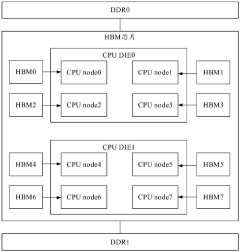
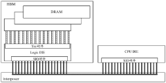
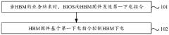
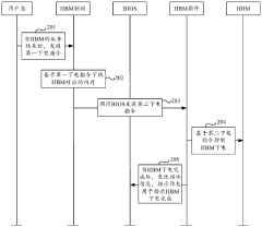
Computer architecture with disaggregated memory and high-bandwidth communication interconnects
PatentActiveUS20240079081A1
Innovation
- A computer system with a unified contiguous memory address space is created, using photonic links for low-power, high-bandwidth communication, where memory is disaggregated from processing units, enabling parallel-access DRAM with automatic packet interleaving and optical interfaces for high-bandwidth data transfer over long distances.


Thermal Management Strategies for HBM Systems
Thermal management represents a critical challenge in HBM systems where high-density memory stacking and intensive data processing generate substantial heat loads. The vertical architecture of HBM modules creates unique thermal dissipation challenges, as heat generated from multiple memory dies must be efficiently removed through limited surface areas. Traditional cooling approaches often prove inadequate for the concentrated thermal loads characteristic of HBM implementations.
Advanced thermal interface materials play a pivotal role in HBM thermal management strategies. High-performance thermal interface materials with thermal conductivities exceeding 5 W/mK are increasingly deployed between memory dies and heat spreaders. These materials, including graphene-enhanced compounds and liquid metal interfaces, facilitate efficient heat transfer from individual memory layers to external cooling systems. The selection of appropriate thermal interface materials directly impacts overall system thermal performance and reliability.
Three-dimensional heat spreading techniques have emerged as essential components of comprehensive thermal management solutions. Integrated heat spreaders utilizing copper or aluminum substrates with optimized fin structures distribute heat across larger surface areas, reducing localized hot spots within HBM stacks. Advanced designs incorporate vapor chamber technology and micro-channel cooling systems that leverage phase-change heat transfer mechanisms for enhanced thermal dissipation efficiency.
Active cooling integration represents the most sophisticated approach to HBM thermal management. Liquid cooling systems with dedicated cold plates and micro-jet impingement cooling provide targeted thermal control for high-performance applications. These systems maintain memory junction temperatures below critical thresholds while enabling sustained high-bandwidth operations. Advanced implementations include closed-loop cooling circuits with real-time temperature monitoring and adaptive flow control mechanisms.
Thermal-aware design methodologies increasingly influence HBM system architecture decisions. Power management strategies incorporate dynamic thermal throttling and workload distribution algorithms that prevent thermal violations while maintaining performance targets. Package-level thermal modeling and simulation tools enable optimization of heat dissipation paths during the design phase, reducing the likelihood of thermal-related performance degradation in deployed systems.
Advanced thermal interface materials play a pivotal role in HBM thermal management strategies. High-performance thermal interface materials with thermal conductivities exceeding 5 W/mK are increasingly deployed between memory dies and heat spreaders. These materials, including graphene-enhanced compounds and liquid metal interfaces, facilitate efficient heat transfer from individual memory layers to external cooling systems. The selection of appropriate thermal interface materials directly impacts overall system thermal performance and reliability.
Three-dimensional heat spreading techniques have emerged as essential components of comprehensive thermal management solutions. Integrated heat spreaders utilizing copper or aluminum substrates with optimized fin structures distribute heat across larger surface areas, reducing localized hot spots within HBM stacks. Advanced designs incorporate vapor chamber technology and micro-channel cooling systems that leverage phase-change heat transfer mechanisms for enhanced thermal dissipation efficiency.
Active cooling integration represents the most sophisticated approach to HBM thermal management. Liquid cooling systems with dedicated cold plates and micro-jet impingement cooling provide targeted thermal control for high-performance applications. These systems maintain memory junction temperatures below critical thresholds while enabling sustained high-bandwidth operations. Advanced implementations include closed-loop cooling circuits with real-time temperature monitoring and adaptive flow control mechanisms.
Thermal-aware design methodologies increasingly influence HBM system architecture decisions. Power management strategies incorporate dynamic thermal throttling and workload distribution algorithms that prevent thermal violations while maintaining performance targets. Package-level thermal modeling and simulation tools enable optimization of heat dissipation paths during the design phase, reducing the likelihood of thermal-related performance degradation in deployed systems.
Advanced Signaling Protocols for Energy-Efficient HBM
Advanced signaling protocols represent a critical frontier in achieving energy-efficient HBM memory interconnect designs. These protocols fundamentally reshape how data transmission occurs between the memory controller and HBM stacks, introducing sophisticated mechanisms that dynamically adjust power consumption based on workload characteristics and performance requirements.
Low-voltage differential signaling (LVDS) variants have emerged as foundational technologies for energy-efficient HBM communication. These protocols operate at reduced voltage swings, typically ranging from 200mV to 400mV compared to traditional 1.2V signaling levels. The implementation of multi-level signaling schemes, such as PAM-4 (Pulse Amplitude Modulation), enables higher data rates while maintaining lower power per bit transmitted. This approach effectively doubles the data throughput without proportionally increasing the energy consumption.
Adaptive signaling protocols introduce dynamic voltage and frequency scaling capabilities specifically tailored for HBM interconnects. These systems continuously monitor traffic patterns and adjust signaling parameters in real-time. During periods of low memory activity, the protocols automatically reduce both voltage levels and clock frequencies, achieving substantial power savings without compromising system responsiveness. The transition mechanisms are designed to minimize latency penalties when scaling back to full performance modes.
Clock gating and power island management protocols have been specifically optimized for HBM architectures. These advanced signaling schemes selectively disable unused channels and memory banks through sophisticated handshaking mechanisms. The protocols implement fine-grained control over individual TSV (Through-Silicon Via) connections, allowing for precise power management at the channel level. This granular approach enables significant energy reductions in applications with non-uniform memory access patterns.
Error correction and signal integrity protocols have been redesigned to maintain reliability while operating at reduced power levels. Advanced forward error correction (FEC) schemes compensate for the increased noise margins associated with low-voltage signaling. These protocols incorporate adaptive equalization and pre-emphasis techniques that optimize signal quality while minimizing the energy overhead typically associated with robust error correction mechanisms.
Emerging protocols are exploring asynchronous signaling methodologies that eliminate the need for continuous clock distribution across HBM stacks. These event-driven communication schemes activate signaling circuits only when data transmission is required, dramatically reducing static power consumption. The protocols implement sophisticated synchronization mechanisms that maintain data integrity while operating in fundamentally different timing domains than traditional synchronous designs.
Low-voltage differential signaling (LVDS) variants have emerged as foundational technologies for energy-efficient HBM communication. These protocols operate at reduced voltage swings, typically ranging from 200mV to 400mV compared to traditional 1.2V signaling levels. The implementation of multi-level signaling schemes, such as PAM-4 (Pulse Amplitude Modulation), enables higher data rates while maintaining lower power per bit transmitted. This approach effectively doubles the data throughput without proportionally increasing the energy consumption.
Adaptive signaling protocols introduce dynamic voltage and frequency scaling capabilities specifically tailored for HBM interconnects. These systems continuously monitor traffic patterns and adjust signaling parameters in real-time. During periods of low memory activity, the protocols automatically reduce both voltage levels and clock frequencies, achieving substantial power savings without compromising system responsiveness. The transition mechanisms are designed to minimize latency penalties when scaling back to full performance modes.
Clock gating and power island management protocols have been specifically optimized for HBM architectures. These advanced signaling schemes selectively disable unused channels and memory banks through sophisticated handshaking mechanisms. The protocols implement fine-grained control over individual TSV (Through-Silicon Via) connections, allowing for precise power management at the channel level. This granular approach enables significant energy reductions in applications with non-uniform memory access patterns.
Error correction and signal integrity protocols have been redesigned to maintain reliability while operating at reduced power levels. Advanced forward error correction (FEC) schemes compensate for the increased noise margins associated with low-voltage signaling. These protocols incorporate adaptive equalization and pre-emphasis techniques that optimize signal quality while minimizing the energy overhead typically associated with robust error correction mechanisms.
Emerging protocols are exploring asynchronous signaling methodologies that eliminate the need for continuous clock distribution across HBM stacks. These event-driven communication schemes activate signaling circuits only when data transmission is required, dramatically reducing static power consumption. The protocols implement sophisticated synchronization mechanisms that maintain data integrity while operating in fundamentally different timing domains than traditional synchronous designs.
Unlock deeper insights with Patsnap Eureka Quick Research — get a full tech report to explore trends and direct your research. Try now!
Generate Your Research Report Instantly with AI Agent
Supercharge your innovation with Patsnap Eureka AI Agent Platform!