

HBM Memory vs Chiplet Architectures: Bandwidth Trade-offs
MAY 18, 20268 MIN READ
Generate Your Research Report Instantly with AI Agent
PatSnap Eureka helps you evaluate technical feasibility & market potential.
HBM and Chiplet Architecture Evolution and Objectives
High Bandwidth Memory (HBM) technology emerged from the critical need to address the growing memory bandwidth bottleneck in high-performance computing applications. Initially developed through a consortium led by SK Hynix and AMD in the early 2010s, HBM represented a paradigm shift from traditional memory architectures by implementing 3D stacking technology and through-silicon vias (TSVs). The first generation HBM achieved 128 GB/s bandwidth per stack, dramatically outperforming conventional GDDR5 memory solutions.
The evolution trajectory of HBM has been marked by successive generations delivering exponential bandwidth improvements. HBM2 introduced in 2016 doubled the bandwidth to 256 GB/s per stack, while HBM2E pushed boundaries further to 460 GB/s. The latest HBM3 generation, commercially available since 2022, achieves unprecedented bandwidth levels exceeding 819 GB/s per stack, establishing new benchmarks for memory-intensive applications.
Parallel to HBM development, chiplet architectures have undergone significant transformation driven by the physical limitations of monolithic chip scaling. AMD's pioneering Zen 2 architecture in 2019 demonstrated the commercial viability of disaggregated processor designs, where specialized functional units are manufactured as separate dies and interconnected through advanced packaging technologies. This approach enables heterogeneous integration of different process nodes optimized for specific functions.
The convergence of HBM and chiplet technologies represents a strategic response to the breakdown of Moore's Law and Dennard Scaling. Modern chiplet designs increasingly incorporate HBM stacks as dedicated memory dies, creating tightly coupled memory-compute complexes that minimize data movement penalties. Intel's Ponte Vecchio and AMD's MI300 series exemplify this integration approach, combining multiple compute chiplets with HBM memory in a single package.
Current technological objectives focus on achieving optimal bandwidth density while managing power consumption and thermal constraints. The industry targets bandwidth scaling beyond 1 TB/s per package through advanced 3D integration techniques and novel interconnect technologies. Simultaneously, chiplet architectures aim to enable modular scalability, allowing system designers to configure memory and compute resources according to specific application requirements while maintaining cost-effectiveness and manufacturing yield advantages.
Market Demand for High-Bandwidth Memory Solutions
The global semiconductor industry is experiencing unprecedented demand for high-bandwidth memory solutions, driven primarily by the explosive growth in artificial intelligence, machine learning, and high-performance computing applications. Data centers processing massive AI workloads require memory systems capable of delivering terabytes per second of bandwidth to feed increasingly complex neural networks and computational models. This surge in computational intensity has created a critical bottleneck where traditional memory architectures can no longer satisfy the bandwidth requirements of modern processors.
Graphics processing units and AI accelerators represent the largest segment driving HBM adoption, as these processors require sustained high-bandwidth data access to maintain computational efficiency. The gaming industry, cryptocurrency mining, and professional visualization markets continue to push bandwidth requirements higher, while emerging applications in autonomous vehicles and edge computing create additional demand vectors. Scientific computing, financial modeling, and real-time analytics applications further amplify the need for memory systems that can deliver consistent, high-throughput data access.
The transition toward chiplet-based processor designs has fundamentally altered memory bandwidth requirements and architectural considerations. Chiplet architectures enable modular processor construction but introduce complex inter-die communication challenges that directly impact memory subsystem design. The bandwidth trade-offs between HBM integration and chiplet connectivity have become critical factors in system-level performance optimization, particularly for applications requiring both high computational throughput and efficient data movement between processing elements.
Enterprise and cloud computing markets are increasingly adopting memory-centric computing paradigms, where bandwidth availability directly correlates with system performance and operational efficiency. The proliferation of in-memory databases, real-time analytics platforms, and distributed computing frameworks has created sustained demand for memory solutions that can support concurrent access patterns from multiple processing units while maintaining low latency characteristics.
Emerging applications in quantum computing simulation, advanced materials research, and climate modeling represent nascent but significant demand drivers for ultra-high-bandwidth memory solutions. These applications require memory systems capable of supporting complex computational workflows that exceed current bandwidth capabilities, creating opportunities for next-generation memory architectures that can bridge the gap between computational requirements and available memory performance.
Current HBM-Chiplet Integration Challenges and Limitations
The integration of HBM memory with chiplet architectures faces significant thermal management challenges that directly impact bandwidth performance. HBM stacks generate substantial heat due to their high-density configuration and intensive data processing operations. When combined with chiplet designs that already present complex thermal profiles, the resulting heat concentration creates hotspots that can throttle memory performance and reduce effective bandwidth utilization.
Signal integrity represents another critical limitation in current HBM-chiplet implementations. The proximity of multiple chiplets to HBM stacks introduces electromagnetic interference and crosstalk issues that degrade signal quality. These interference patterns become particularly problematic at higher frequencies, forcing designers to implement conservative timing margins that ultimately limit achievable bandwidth rates.
Power delivery network complexity poses substantial constraints on HBM-chiplet integration effectiveness. Each HBM stack requires precise voltage regulation and current delivery, while chiplets demand their own power management systems. The interaction between these power domains creates voltage ripple and noise issues that can cause memory access latencies to increase unpredictably, reducing overall bandwidth efficiency.
Physical routing constraints significantly limit the scalability of HBM-chiplet configurations. The dense interconnect requirements between chiplets and HBM controllers create routing congestion that forces longer signal paths and additional via structures. These extended routing paths introduce parasitic capacitance and inductance that degrade signal timing and limit maximum operating frequencies.
Manufacturing yield challenges emerge from the complexity of integrating multiple advanced packaging technologies simultaneously. HBM stacking processes must align precisely with chiplet placement and interposer fabrication, creating multiple points of potential failure. Lower yields translate to higher costs and reduced commercial viability for high-bandwidth HBM-chiplet solutions.
Standardization gaps in interface protocols between different chiplet vendors and HBM suppliers create compatibility issues that limit bandwidth optimization opportunities. Without unified standards for cache coherency, memory mapping, and bandwidth allocation across heterogeneous chiplet configurations, system designers cannot fully exploit the theoretical bandwidth capabilities of HBM memory in multi-chiplet environments.
Existing HBM-Chiplet Bandwidth Optimization Approaches
01 High Bandwidth Memory (HBM) interface optimization and control mechanisms
Advanced control mechanisms and interface optimizations for HBM systems focus on improving data transfer efficiency through enhanced memory controllers, optimized signaling protocols, and intelligent bandwidth allocation. These techniques include dynamic frequency scaling, adaptive power management, and sophisticated error correction methods to maximize throughput while maintaining system stability.- High Bandwidth Memory (HBM) interface optimization and control mechanisms: Advanced control mechanisms and interface optimizations for HBM systems focus on improving data transfer efficiency through enhanced memory controllers, optimized signaling protocols, and intelligent bandwidth allocation. These techniques include dynamic frequency scaling, adaptive power management, and sophisticated error correction methods to maximize throughput while maintaining system stability and reducing latency in high-performance computing applications.
- Chiplet interconnect architectures and communication protocols: Chiplet-based designs utilize advanced interconnect architectures that enable multiple processing units to communicate efficiently across different dies. These architectures implement specialized communication protocols, routing mechanisms, and network-on-chip solutions that optimize data flow between chiplets while minimizing power consumption and maximizing aggregate bandwidth performance in heterogeneous computing systems.
- Memory bandwidth optimization through advanced packaging and stacking technologies: Three-dimensional memory stacking and advanced packaging technologies enable significant bandwidth improvements by reducing signal path lengths and increasing parallel data channels. These approaches incorporate through-silicon vias, advanced bump technologies, and optimized thermal management solutions to achieve higher memory densities and improved performance characteristics in compact form factors.
- Dynamic bandwidth allocation and traffic management systems: Intelligent bandwidth management systems implement dynamic allocation algorithms that monitor traffic patterns and adjust resource distribution in real-time. These systems utilize predictive analytics, quality-of-service mechanisms, and adaptive scheduling to optimize memory access patterns and prevent bottlenecks, ensuring efficient utilization of available bandwidth across multiple processing elements and memory hierarchies.
- Power-efficient bandwidth scaling and thermal management: Power-aware bandwidth scaling techniques focus on maintaining high performance while minimizing energy consumption through intelligent voltage and frequency scaling, thermal-aware routing, and adaptive power gating mechanisms. These solutions incorporate real-time monitoring of thermal conditions and power consumption to dynamically adjust operating parameters, ensuring optimal performance per watt in bandwidth-intensive applications.
02 Chiplet interconnect architectures and communication protocols
Chiplet-based designs utilize specialized interconnect architectures that enable high-speed communication between multiple semiconductor dies. These architectures implement advanced routing algorithms, packet-based communication protocols, and mesh or ring topologies to achieve optimal bandwidth utilization across chiplet boundaries while minimizing latency and power consumption.Expand Specific Solutions03 Memory bandwidth optimization through advanced caching and prefetching
Sophisticated caching strategies and predictive prefetching mechanisms are employed to maximize effective memory bandwidth utilization. These approaches include multi-level cache hierarchies, intelligent data placement algorithms, and machine learning-based prediction models that anticipate memory access patterns to reduce latency and improve overall system performance.Expand Specific Solutions04 3D stacking and through-silicon via (TSV) technologies for bandwidth enhancement
Three-dimensional memory stacking technologies utilize vertical integration and through-silicon vias to dramatically increase memory bandwidth density. These implementations feature advanced thermal management, optimized electrical routing, and novel packaging techniques that enable multiple memory layers to operate simultaneously while maintaining signal integrity and thermal stability.Expand Specific Solutions05 Network-on-chip (NoC) designs for multi-chiplet bandwidth management
Network-on-chip architectures provide scalable communication infrastructure for multi-chiplet systems, implementing sophisticated routing protocols, quality-of-service mechanisms, and congestion control algorithms. These designs enable efficient bandwidth sharing among multiple processing elements while providing deterministic performance guarantees and fault tolerance capabilities.Expand Specific Solutions
Leading Companies in HBM and Chiplet Markets
The HBM memory versus chiplet architectures bandwidth trade-off represents a rapidly evolving competitive landscape in the mature semiconductor industry, driven by AI and high-performance computing demands. The market, valued at billions globally, features established memory giants like Samsung, Micron, and ChangXin Memory Technologies dominating HBM production, while chiplet innovation is led by AMD, Intel, and emerging players like Luminous Computing and AvicenaTech. Technology maturity varies significantly - HBM has reached commercial deployment across data centers, whereas chiplet architectures remain in advanced development phases. Traditional players like IBM, Huawei, and TSMC provide foundational infrastructure, while specialized companies such as Rambus and Synopsys offer critical IP and design tools. The competitive dynamics reflect a transition from monolithic designs to disaggregated architectures, with bandwidth optimization becoming the key differentiator for next-generation computing systems.
Samsung Electronics Co., Ltd.
Technical Solution: Samsung has developed advanced HBM3E memory technology offering up to 1.15TB/s bandwidth per stack with 36GB capacity, representing a significant leap in memory performance for AI and high-performance computing applications. Their approach focuses on through-silicon via (TSV) technology and advanced packaging to achieve higher bandwidth density while maintaining power efficiency. Samsung's HBM solutions are designed to work seamlessly with chiplet architectures, providing optimized interconnect solutions that minimize latency between memory and processing units. The company has also invested heavily in co-packaging technologies that enable tighter integration between HBM stacks and compute chiplets, reducing signal propagation delays and improving overall system bandwidth utilization.
Strengths: Market leadership in HBM production with proven high-volume manufacturing capabilities and strong partnerships with major processor vendors. Weaknesses: Higher cost compared to traditional memory solutions and dependency on advanced packaging technologies that require significant capital investment.
Micron Technology, Inc.
Technical Solution: Micron has developed comprehensive HBM3E solutions delivering up to 1.2TB/s per stack bandwidth with enhanced power efficiency for AI workloads and data center applications. Their technical approach emphasizes thermal management and signal integrity optimization in chiplet environments, utilizing advanced substrate technologies and innovative cooling solutions. Micron's HBM architecture incorporates adaptive bandwidth allocation mechanisms that can dynamically adjust memory access patterns based on chiplet workload demands. The company has also pioneered near-data computing capabilities within HBM modules, enabling certain processing operations to occur closer to memory storage, thereby reducing bandwidth requirements for specific computational tasks and improving overall system efficiency in multi-chiplet configurations.
Strengths: Strong focus on power efficiency and thermal management with extensive experience in enterprise memory solutions. Weaknesses: Smaller market share compared to Samsung and challenges in competing on cost for high-volume applications.
Key Patents in HBM-Chiplet Interconnect Technologies
System and method for modular HBM chiplet architecture
PatentPendingEP4621582A1
Innovation
- A modular HBM design utilizing daisy-chain and network-grid configurations to interconnect multiple HBM chiplets, allowing scalable memory bandwidth and capacity expansion.


Optically interconnected high bandwidth memory architectures
PatentWO2024215908A1
Innovation
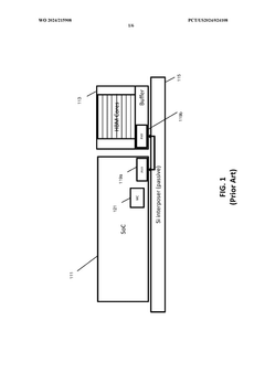
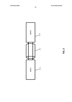
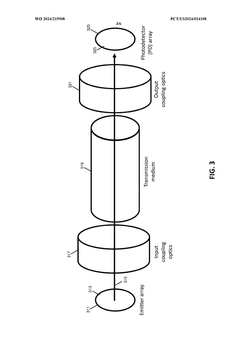
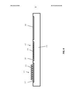
- The implementation of optically interconnected high bandwidth memory architectures using multi-chip packages with optical interfaces and transmission media, such as optical fibers, to enable longer interconnects between System-on-Chip (SoC) and HBM, allowing for increased memory capacity and reduced thermal stress by physically separating HBM from the hot SoC.
Thermal Management in High-Bandwidth Memory Systems
Thermal management represents one of the most critical challenges in high-bandwidth memory systems, particularly when comparing HBM implementations with chiplet architectures. The exponential increase in data throughput demands creates substantial heat generation that directly impacts system performance, reliability, and bandwidth sustainability.
HBM memory stacks generate significant thermal loads due to their vertical integration and high-speed operation. The three-dimensional structure inherently creates thermal hotspots, as heat dissipation becomes increasingly difficult through the stacked die configuration. Each memory layer contributes to cumulative heat buildup, with the middle layers experiencing the most severe thermal stress due to limited heat escape paths.
Chiplet architectures present distinct thermal characteristics compared to monolithic HBM designs. The distributed nature of chiplet implementations allows for more effective heat spreading across the package substrate. Individual chiplets can be thermally optimized independently, enabling targeted cooling solutions for high-power components while maintaining efficient thermal pathways for memory interfaces.
Advanced thermal interface materials play crucial roles in both architectures. HBM systems require specialized thermal solutions including through-silicon vias for vertical heat conduction and micro-channel cooling systems. Chiplet designs benefit from optimized thermal interface materials between individual dies and enhanced package-level thermal management through improved substrate designs and heat spreader configurations.
Temperature gradients significantly impact bandwidth performance in both systems. HBM memory exhibits temperature-dependent timing variations that can reduce effective bandwidth by 15-25% under thermal stress conditions. Chiplet architectures demonstrate more predictable thermal behavior, allowing for dynamic bandwidth allocation based on real-time temperature monitoring across distributed memory controllers.
Emerging thermal management solutions include integrated liquid cooling systems, phase-change materials, and advanced packaging techniques such as embedded cooling channels. These innovations are essential for maintaining optimal bandwidth performance while ensuring long-term reliability in next-generation high-bandwidth memory implementations across both HBM and chiplet architectural approaches.
Power Efficiency Trade-offs in HBM-Chiplet Designs
The integration of High Bandwidth Memory (HBM) with chiplet architectures presents significant power efficiency challenges that directly impact the bandwidth advantages these systems aim to achieve. The fundamental trade-off emerges from the inherent power consumption characteristics of both HBM stacks and the interconnect infrastructure required for chiplet communication.
HBM memory modules, while delivering exceptional bandwidth performance, consume substantially more power per bit compared to traditional DDR memory solutions. The Through Silicon Via (TSV) technology and the complex 3D stacking architecture contribute to elevated static power consumption, typically ranging from 15-25 watts per HBM stack under full operational load. This power overhead becomes particularly pronounced in multi-chiplet systems where multiple HBM stacks are distributed across different chiplets to maximize memory bandwidth.
The chiplet interconnect fabric introduces additional power consumption layers that compound the overall energy efficiency challenges. High-speed SerDes links, coherency protocols, and packet routing mechanisms required for inter-chiplet communication can consume 2-5 watts per high-bandwidth link operating at speeds exceeding 25 Gbps. As bandwidth requirements increase, the number of active links scales proportionally, creating a direct correlation between bandwidth capacity and power consumption.
Thermal management becomes a critical constraint in HBM-chiplet configurations, as the concentrated heat generation from both memory stacks and chiplet processing units can lead to thermal throttling. This thermal limitation often forces systems to operate below peak bandwidth capacity to maintain acceptable junction temperatures, effectively reducing the practical bandwidth utilization to 70-80% of theoretical maximum.
Power delivery network complexity further exacerbates efficiency challenges, as HBM stacks require multiple voltage domains with tight regulation tolerances. The distributed nature of chiplet architectures necessitates sophisticated power management units and voltage regulators, introducing additional conversion losses that can reduce overall system efficiency by 10-15%.
Advanced power management techniques, including dynamic voltage and frequency scaling for both HBM controllers and chiplet interconnects, offer potential mitigation strategies. However, these solutions introduce latency penalties that can impact the effective bandwidth utilization, creating a secondary trade-off between power efficiency and performance consistency in bandwidth-critical applications.
Unlock deeper insights with PatSnap Eureka Quick Research — get a full tech report to explore trends and direct your research. Try now!
Generate Your Research Report Instantly with AI Agent
Supercharge your innovation with PatSnap Eureka AI Agent Platform!