

Compare HBM Memory vs CPU Cache Access Times for AI Tasks
MAY 18, 20269 MIN READ
Generate Your Research Report Instantly with AI Agent
PatSnap Eureka helps you evaluate technical feasibility & market potential.
HBM Memory and CPU Cache Technology Background and Objectives
The evolution of memory technologies has been fundamentally driven by the exponential growth in computational demands, particularly in artificial intelligence applications. High Bandwidth Memory (HBM) emerged as a revolutionary solution to address the memory wall problem that has plagued computing systems for decades. This advanced memory architecture represents a paradigm shift from traditional memory designs, offering unprecedented bandwidth capabilities through innovative 3D stacking and through-silicon via (TSV) technology.
CPU cache systems have undergone continuous refinement since their introduction in the 1960s, evolving from simple direct-mapped structures to sophisticated multi-level hierarchies. Modern processors incorporate complex cache architectures featuring L1, L2, and L3 levels, each optimized for specific access patterns and latency requirements. The development trajectory has consistently focused on minimizing access times while maximizing hit rates through advanced prediction algorithms and prefetching mechanisms.
The convergence of AI workloads and memory system design has created unprecedented challenges in data movement and processing efficiency. Traditional memory hierarchies, originally designed for general-purpose computing, face significant limitations when handling the massive datasets and parallel processing requirements characteristic of machine learning algorithms. Neural network training and inference operations demand sustained high-bandwidth memory access patterns that exceed the capabilities of conventional DDR-based systems.
HBM technology addresses these limitations through its unique architectural approach, utilizing vertically stacked DRAM dies connected via high-speed interfaces. This design enables bandwidth capabilities exceeding 1TB/s while maintaining relatively compact form factors. The technology has progressed through multiple generations, with HBM3 achieving significant improvements in both bandwidth and energy efficiency compared to its predecessors.
The primary objective of comparing HBM memory and CPU cache access times centers on optimizing AI task performance through informed memory subsystem design decisions. Understanding the latency characteristics, bandwidth capabilities, and energy consumption profiles of these technologies enables system architects to make strategic choices that maximize computational throughput while minimizing bottlenecks.
Contemporary AI applications exhibit diverse memory access patterns, from the sequential data streaming required for large language model inference to the random access patterns typical of graph neural networks. Each pattern presents unique challenges that must be addressed through appropriate memory hierarchy design. The objective extends beyond simple performance metrics to encompass power efficiency, thermal management, and scalability considerations essential for next-generation AI systems.
Market Demand Analysis for High-Performance AI Memory Solutions
The global artificial intelligence market is experiencing unprecedented growth, driving substantial demand for high-performance memory solutions that can effectively bridge the performance gap between processing units and data storage. This surge is primarily fueled by the proliferation of large language models, computer vision applications, and real-time inference systems that require massive computational throughput and minimal latency constraints.
Enterprise adoption of AI workloads has created a critical bottleneck in memory subsystem performance, where traditional memory hierarchies struggle to meet the bandwidth and latency requirements of modern neural network architectures. Organizations deploying transformer-based models, deep learning training pipelines, and edge AI applications are increasingly seeking memory solutions that can deliver consistent performance at scale while maintaining cost-effectiveness.
The demand landscape is particularly pronounced in cloud service providers, autonomous vehicle manufacturers, and high-frequency trading firms, where memory access patterns directly impact revenue generation and operational efficiency. These sectors require memory solutions capable of handling irregular access patterns, large working sets, and sustained high-bandwidth operations that exceed the capabilities of conventional memory architectures.
Data center operators are experiencing growing pressure to optimize total cost of ownership while supporting increasingly memory-intensive AI workloads. The economic imperative extends beyond raw performance metrics to encompass power efficiency, thermal management, and infrastructure scalability. Memory solutions that can reduce the number of required processing nodes while maintaining performance targets represent significant operational advantages.
Emerging applications in real-time AI inference, particularly in autonomous systems and industrial automation, are creating new market segments with stringent latency requirements. These applications demand memory architectures that can guarantee predictable access times while supporting the parallel processing patterns characteristic of modern AI algorithms.
The market trajectory indicates sustained growth in demand for specialized memory solutions that can address the unique characteristics of AI workloads, including their tendency toward high spatial and temporal locality, burst access patterns, and sensitivity to memory bandwidth limitations. This demand is reshaping memory architecture priorities and driving innovation in both hardware design and system integration approaches.
Current State and Challenges of Memory Hierarchy in AI Systems
The memory hierarchy in AI systems represents a complex ecosystem where different storage technologies serve distinct roles in computational workflows. At the foundation lies system memory, primarily composed of DDR4/DDR5 DRAM, which provides the baseline storage for model parameters and datasets. Above this sits High Bandwidth Memory (HBM), strategically positioned as an intermediate layer offering substantially higher throughput than conventional DRAM while maintaining reasonable capacity. At the apex of this hierarchy, CPU and GPU caches deliver ultra-low latency access to frequently used data through sophisticated prediction algorithms.
Current AI workloads expose fundamental limitations in traditional memory architectures. Large language models and deep neural networks demand simultaneous access to vast parameter sets, creating unprecedented pressure on memory bandwidth. The disparity between computational capability and memory performance has widened significantly, with modern AI accelerators capable of processing data far faster than conventional memory systems can supply it. This bottleneck manifests particularly acutely during inference operations where model weights must be continuously accessed across multiple processing units.
HBM technology has emerged as a critical solution, delivering bandwidth exceeding 1TB/s compared to DDR5's theoretical maximum of 51.2GB/s per channel. However, HBM integration presents substantial challenges including thermal management, manufacturing complexity, and cost considerations. The technology requires sophisticated packaging techniques such as through-silicon vias and interposer-based designs, limiting its adoption to high-end applications where performance justifies the premium.
Cache hierarchies face their own set of constraints in AI contexts. Traditional cache optimization strategies, designed for general-purpose computing patterns, often prove ineffective for AI workloads characterized by streaming data access and limited temporal locality. The massive datasets typical in machine learning frequently exceed cache capacities, reducing hit rates and forcing frequent main memory accesses. Additionally, the parallel nature of AI computations creates cache coherency challenges across multiple processing cores.
Power consumption emerges as another critical constraint, particularly in edge AI deployments where energy efficiency directly impacts system viability. HBM's high performance comes at the cost of increased power draw, while cache misses trigger expensive DRAM accesses that compound energy consumption. The challenge intensifies in mobile and embedded AI applications where thermal and battery constraints severely limit available power budgets.
Scalability issues further complicate the landscape as AI models continue growing exponentially. Current memory architectures struggle to accommodate models approaching trillion-parameter scales while maintaining acceptable performance characteristics. The physical limitations of memory bandwidth and the economic constraints of HBM deployment create a sustainability challenge for continued AI advancement.
Current Memory Access Solutions for AI Task Optimization
01 Cache memory architecture and organization
Various cache memory architectures are designed to optimize data access patterns and reduce latency between the processor and main memory. These architectures include multi-level cache hierarchies, associative cache designs, and specialized cache organization methods that improve overall system performance by storing frequently accessed data closer to the CPU.- Cache memory architecture and organization: Various cache memory architectures are designed to optimize data access patterns and reduce latency between the processor and main memory. These architectures include multi-level cache hierarchies, associative cache designs, and specialized cache organizations that improve hit rates and reduce access times through strategic data placement and retrieval mechanisms.
- Memory access timing optimization techniques: Techniques for optimizing memory access timing involve sophisticated scheduling algorithms, predictive caching mechanisms, and timing control circuits that minimize latency in memory operations. These methods focus on reducing wait states, improving memory bandwidth utilization, and coordinating access patterns between different memory subsystems to achieve optimal performance.
- High bandwidth memory interface design: High bandwidth memory interfaces incorporate advanced signaling protocols, parallel data paths, and sophisticated memory controllers to achieve maximum data throughput. These designs address the challenges of maintaining signal integrity at high frequencies while providing multiple channels for concurrent data transfer, enabling significant improvements in memory subsystem performance.
- Cache coherency and synchronization mechanisms: Cache coherency protocols ensure data consistency across multiple cache levels and processing units by implementing sophisticated synchronization mechanisms. These systems manage cache line states, handle invalidation protocols, and coordinate memory updates to maintain data integrity while maximizing cache utilization and minimizing access conflicts.
- Memory controller and arbitration systems: Memory controllers and arbitration systems manage access requests from multiple sources, implementing priority schemes and scheduling algorithms to optimize memory utilization. These systems handle request queuing, bandwidth allocation, and conflict resolution to ensure efficient memory access while maintaining system performance and preventing bottlenecks in high-performance computing environments.
02 Memory access timing optimization techniques
Techniques for optimizing memory access timing involve sophisticated algorithms and hardware mechanisms that predict and prefetch data, manage memory bandwidth allocation, and coordinate between different memory subsystems. These methods focus on reducing wait states and improving the efficiency of data transfers between high-bandwidth memory and processing units.Expand Specific Solutions03 High-bandwidth memory interface design
High-bandwidth memory interfaces are specifically designed to handle massive data throughput requirements of modern computing systems. These interfaces incorporate advanced signaling protocols, parallel data paths, and sophisticated timing control mechanisms to achieve maximum data transfer rates while maintaining signal integrity and minimizing access latency.Expand Specific Solutions04 Cache coherency and synchronization mechanisms
Cache coherency protocols ensure data consistency across multiple cache levels and processing units in complex computing systems. These mechanisms include various synchronization methods, invalidation protocols, and coherency maintenance algorithms that prevent data corruption while maintaining optimal access performance across distributed cache hierarchies.Expand Specific Solutions05 Memory controller and scheduling algorithms
Advanced memory controllers implement sophisticated scheduling algorithms to manage concurrent memory requests from multiple sources. These systems optimize memory access patterns, handle priority-based request queuing, and coordinate between different memory types to maximize throughput while minimizing latency for critical operations.Expand Specific Solutions
Major Players in HBM and CPU Cache Technology Landscape
The HBM memory versus CPU cache access time comparison for AI tasks represents a rapidly evolving competitive landscape within the mature semiconductor industry. The market is experiencing significant growth driven by AI workload demands, with established players like Samsung Electronics, Micron Technology, and Intel leading HBM development alongside NVIDIA's GPU integration expertise. Technology maturity varies significantly - while CPU cache architectures are well-established, HBM technology is advancing rapidly with companies like Samsung and Micron pushing HBM3 and beyond. The competitive dynamics show traditional memory manufacturers competing with AI-focused companies, while emerging players like Shanghai Biren Technology and established giants like Huawei Technologies are developing integrated solutions that optimize both memory hierarchies for AI-specific workloads.
International Business Machines Corp.
Technical Solution: IBM has developed advanced memory hierarchy solutions that integrate HBM with traditional CPU cache systems in their POWER processors and AI accelerators. Their approach utilizes coherent memory interfaces and advanced prefetching algorithms to optimize data movement between CPU cache layers and HBM memory. IBM's research demonstrates practical implementations where CPU cache handles latency-critical operations (1-4ns for L1, 15-30ns for L2) while HBM manages bandwidth-intensive AI computations with 300-500ns latency but superior parallel access capabilities. Their Memory Inception technology and AI-optimized memory controllers implement intelligent caching strategies that predict AI workload memory access patterns, effectively bridging the performance gap between fast CPU cache and high-capacity HBM memory for enterprise AI applications.
Strengths: Advanced memory hierarchy integration, strong enterprise AI focus, sophisticated memory management algorithms. Weaknesses: Limited consumer market presence, complex system architecture, higher implementation costs for smaller scale deployments.
Samsung Electronics Co., Ltd.
Technical Solution: Samsung serves as a primary manufacturer of HBM memory modules, developing HBM2E and HBM3 technologies with focus on AI applications. Their HBM solutions achieve memory bandwidth of up to 819GB/s per stack with reduced access latencies optimized for machine learning workloads. Samsung's approach involves advanced packaging technologies like Through-Silicon Via (TSV) and micro-bump interconnects to minimize signal propagation delays. They have developed specialized HBM variants for AI accelerators that balance capacity, bandwidth, and power efficiency, typically offering 16GB-24GB per stack configurations. Their memory controllers implement advanced prefetching and caching mechanisms to bridge the latency gap between HBM and CPU cache systems.
Strengths: Leading HBM manufacturing capabilities, advanced packaging technologies, high memory density. Weaknesses: Limited direct AI system integration, dependency on third-party processor designs, complex thermal management requirements.
Core Technical Innovations in HBM vs CPU Cache Design
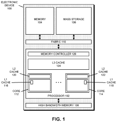
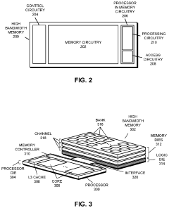
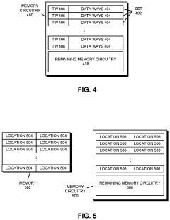
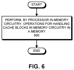
Performing Operations for Handling Data using Processor in Memory Circuitry in a High Bandwidth Memory
PatentInactiveUS20230359556A1
Innovation
- Implementing processor in memory (PIM) circuitry within high bandwidth memory to perform cache operations and handle data, reducing the need for processors to handle these tasks directly, thereby offloading operations and improving performance.
Memory access request processing method, system on chip, storage medium and program product
PatentActiveCN121301277A
Innovation
- By detecting consecutive memory access requests and triggering a continuous transfer mode, and utilizing precise remapping of the physical address bit field, the memory controller identifier is uniformly pointed to the same target memory controller, thereby achieving centralized routing of all consecutive requests and reducing memory controller switching.


Performance Benchmarking Methodologies for AI Memory Systems
Establishing comprehensive performance benchmarking methodologies for AI memory systems requires a multi-dimensional approach that addresses the unique characteristics of both HBM memory and CPU cache architectures. The fundamental challenge lies in creating standardized measurement frameworks that can accurately capture the performance differences across varying AI workload patterns and computational intensities.
The primary benchmarking methodology centers on latency measurement protocols that distinguish between sequential and random access patterns. For HBM memory evaluation, benchmarks must account for the parallel nature of memory channels and the impact of memory controller scheduling algorithms. CPU cache benchmarking requires consideration of cache hierarchy levels, prefetching mechanisms, and cache coherency protocols that significantly influence access times during AI computations.
Throughput-based benchmarking represents another critical methodology dimension, particularly relevant for AI tasks involving large-scale matrix operations and tensor computations. These benchmarks should measure sustained bandwidth under various data access patterns, including streaming workloads typical in neural network inference and training phases. The methodology must incorporate burst transfer capabilities and evaluate performance degradation under thermal throttling conditions.
Workload-specific benchmarking methodologies are essential for capturing real-world AI performance characteristics. This includes developing synthetic benchmarks that replicate common AI operations such as convolution layers, attention mechanisms, and gradient computations. The benchmarks should vary in data locality patterns, from highly localized operations that benefit from cache proximity to memory-intensive operations that require high-bandwidth access to large datasets.
Power efficiency benchmarking methodologies add another crucial dimension, measuring performance per watt across different memory access patterns. This involves correlating access latency and throughput measurements with power consumption data, enabling comprehensive evaluation of energy efficiency trade-offs between HBM and cache-based approaches for specific AI workloads.
Statistical analysis methodologies must account for the variability inherent in modern memory systems, incorporating confidence intervals and outlier detection to ensure benchmark reliability. The methodology should include automated test harnesses capable of running extended benchmark suites while monitoring system stability and thermal conditions that could influence results.
Energy Efficiency Considerations in AI Memory Design
Energy efficiency has emerged as a critical design consideration in AI memory architectures, particularly when comparing HBM memory and CPU cache systems. The exponential growth in AI computational demands has intensified focus on power consumption optimization, as memory subsystems can account for 40-60% of total system power in modern AI accelerators.
HBM memory demonstrates superior energy efficiency in bulk data operations through its wide parallel interface architecture. The 1024-bit bus width enables simultaneous transfer of large data blocks, reducing the number of memory transactions required per unit of data processed. This architectural advantage translates to lower energy per bit transferred, typically achieving 15-20 pJ/bit compared to traditional GDDR memory's 25-30 pJ/bit. The reduced voltage operation at 1.2V further contributes to power savings in high-bandwidth scenarios.
CPU cache systems exhibit different energy characteristics optimized for frequent, small-scale access patterns. L1 caches operate at extremely low energy levels, consuming approximately 0.5-1 pJ per access due to their proximity to processing cores and optimized SRAM technology. However, cache miss penalties introduce significant energy overhead, as data retrieval from lower cache levels or main memory can consume 100-1000x more energy than successful L1 hits.
The energy efficiency comparison becomes particularly nuanced in AI workload contexts. Transformer models and large neural networks benefit from HBM's energy-efficient bulk transfers during weight loading and activation propagation phases. Conversely, inference tasks with high data locality favor CPU cache systems, where repeated access to small parameter sets leverages the ultra-low energy characteristics of on-chip memory.
Dynamic voltage and frequency scaling technologies further complicate energy comparisons. Modern HBM implementations incorporate adaptive power management, reducing voltage during low-activity periods. Similarly, CPU cache systems employ power gating and clock gating techniques to minimize static power consumption during idle cycles.
Emerging memory technologies are reshaping energy efficiency paradigms. Processing-in-memory approaches integrated with HBM reduce data movement energy by performing computations directly within memory arrays. Near-data computing architectures similarly minimize energy overhead by positioning processing elements adjacent to cache structures, reducing interconnect power consumption in AI-specific operations.
Unlock deeper insights with PatSnap Eureka Quick Research — get a full tech report to explore trends and direct your research. Try now!
Generate Your Research Report Instantly with AI Agent
Supercharge your innovation with PatSnap Eureka AI Agent Platform!