

How to Align Thermal Sensors with HBM Memory Interface Layers
MAY 18, 20269 MIN READ
Generate Your Research Report Instantly with AI Agent
PatSnap Eureka helps you evaluate technical feasibility & market potential.
Thermal Management in HBM Systems Background and Objectives
High Bandwidth Memory (HBM) technology has emerged as a critical solution for addressing the ever-increasing memory bandwidth demands of modern computing systems, particularly in high-performance computing, artificial intelligence, and graphics processing applications. The evolution from traditional memory architectures to HBM represents a paradigm shift toward three-dimensional memory stacking, where multiple DRAM dies are vertically integrated through silicon vias to achieve unprecedented data transfer rates exceeding 460 GB/s per stack.
The fundamental challenge in HBM systems lies in the inherent thermal complexity introduced by the vertical stacking architecture. Unlike conventional planar memory designs, HBM stacks concentrate significant power density within a compact footprint, creating localized hotspots that can severely impact performance, reliability, and longevity. The thermal gradient across different memory layers varies substantially, with upper layers typically experiencing higher temperatures due to heat accumulation from lower layers and reduced heat dissipation pathways.
Thermal management in HBM systems requires precise monitoring and control mechanisms to maintain optimal operating conditions across all memory interface layers. The alignment of thermal sensors with specific HBM interface layers presents a multifaceted technical challenge that encompasses sensor placement optimization, thermal coupling efficiency, and real-time temperature monitoring accuracy. Misaligned thermal sensors can lead to inadequate thermal characterization, resulting in suboptimal thermal management strategies and potential system failures.
The primary objective of this research focuses on developing methodologies and technologies to achieve precise thermal sensor alignment with HBM memory interface layers. This involves establishing optimal sensor positioning strategies that account for the three-dimensional thermal distribution patterns within HBM stacks, ensuring accurate temperature measurement across all memory layers while minimizing interference with normal memory operations.
Secondary objectives include developing advanced sensor integration techniques that maintain the structural integrity of HBM packages while providing comprehensive thermal monitoring capabilities. The research aims to establish standardized alignment protocols that can be implemented across different HBM generations and manufacturers, ensuring consistent thermal management performance regardless of specific implementation variations.
The ultimate goal encompasses creating a robust thermal management framework that enables proactive thermal control, prevents thermal-induced performance degradation, and extends the operational lifespan of HBM systems through intelligent sensor-driven thermal regulation strategies.
Market Demand for Advanced HBM Thermal Solutions
The semiconductor industry is experiencing unprecedented demand for high-performance computing solutions, driving significant market interest in advanced High Bandwidth Memory thermal management technologies. Data centers, artificial intelligence accelerators, and high-performance computing systems increasingly rely on HBM modules to achieve superior memory bandwidth and capacity. However, the compact stacking architecture of HBM presents substantial thermal challenges that require sophisticated sensor alignment solutions.
Enterprise customers in cloud computing and hyperscale data center markets represent the primary demand drivers for advanced HBM thermal solutions. These organizations face mounting pressure to maximize computational density while maintaining system reliability and performance consistency. The thermal management of HBM stacks has become a critical bottleneck, as inadequate temperature monitoring can lead to performance throttling, reduced system lifespan, and potential data integrity issues.
The artificial intelligence and machine learning sectors demonstrate particularly strong demand for precise thermal sensor alignment technologies. Training large language models and executing complex neural network computations generate substantial heat loads within HBM modules. Companies developing AI accelerators require thermal solutions that can accurately monitor temperature variations across different memory interface layers to prevent thermal runaway conditions and maintain optimal performance.
Graphics processing and gaming markets also contribute significantly to the demand landscape. High-end graphics cards incorporating HBM memory face thermal constraints that directly impact gaming performance and professional visualization applications. Graphics card manufacturers seek thermal sensor alignment solutions that enable real-time temperature monitoring and dynamic thermal management across HBM interface layers.
The automotive industry represents an emerging demand segment, particularly for autonomous driving systems and advanced driver assistance technologies. These applications require HBM modules to operate reliably across wide temperature ranges while maintaining strict safety standards. Precise thermal sensor alignment becomes essential for ensuring consistent memory performance in challenging automotive environments.
Market demand is further amplified by regulatory requirements and industry standards emphasizing system reliability and energy efficiency. Organizations must demonstrate effective thermal management capabilities to meet compliance requirements and achieve sustainability goals. Advanced HBM thermal solutions that provide accurate temperature monitoring across interface layers enable better energy optimization and system longevity.
The growing complexity of multi-chip module designs and heterogeneous computing architectures creates additional market opportunities. System integrators require thermal solutions that can accommodate diverse HBM configurations and interface specifications while providing consistent monitoring capabilities across different memory layers and chip architectures.
Current Thermal Sensor Alignment Challenges in HBM Stacks
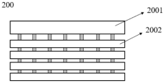
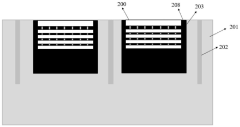
High Bandwidth Memory (HBM) stacks present unprecedented thermal management challenges due to their three-dimensional architecture and extreme integration density. The vertical stacking of multiple DRAM dies creates complex thermal gradients that vary significantly across different layers and interface regions. Traditional thermal monitoring approaches, designed for planar memory architectures, prove inadequate for capturing the nuanced thermal behavior within HBM stacks, where heat generation and dissipation patterns differ substantially from conventional memory solutions.
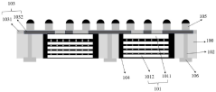
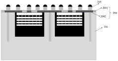
The primary alignment challenge stems from the microscale precision required to position thermal sensors at critical interface layers within the HBM stack. Each interface between DRAM dies represents a potential thermal bottleneck, yet accessing these regions for sensor placement requires navigating through-silicon vias (TSVs), microbumps, and interconnect structures that occupy minimal physical space. The geometric constraints imposed by the 1024-bit wide interface and the need to maintain signal integrity create severe limitations on sensor positioning options.
Thermal sensor placement accuracy becomes critically important when considering the thermal coupling effects between adjacent layers. Misaligned sensors can provide misleading temperature readings that fail to capture localized hotspots or thermal gradients across interface boundaries. The challenge is compounded by manufacturing tolerances in the die stacking process, where even minor variations in layer alignment can significantly impact thermal sensor effectiveness and measurement accuracy.
Signal routing complexity represents another significant obstacle in thermal sensor alignment. The dense interconnect environment within HBM stacks leaves limited routing resources for thermal monitoring circuits. Sensor signals must compete with high-speed data paths while avoiding electromagnetic interference that could compromise both thermal measurements and memory performance. This constraint often forces suboptimal sensor placement decisions that prioritize routing feasibility over thermal monitoring effectiveness.
The dynamic nature of thermal behavior in HBM stacks further complicates sensor alignment strategies. Temperature distributions shift rapidly based on memory access patterns, workload characteristics, and external cooling conditions. Static sensor placement approaches may miss critical thermal events or fail to provide adequate coverage during peak thermal stress conditions, necessitating adaptive alignment methodologies that can respond to changing thermal landscapes.
Manufacturing process variations introduce additional uncertainty into thermal sensor alignment. The inherent tolerances in die bonding, TSV formation, and microbump placement create positional uncertainties that can render precisely designed sensor layouts ineffective. These variations require robust alignment strategies that maintain thermal monitoring capability despite manufacturing-induced deviations from nominal positioning.
Existing Thermal Sensor Integration Solutions for HBM
01 Optical alignment systems for thermal sensors
Methods and systems for aligning thermal sensors using optical components such as lenses, mirrors, and optical fibers. These systems utilize light-based alignment techniques to precisely position thermal sensors relative to target objects or reference points. The optical alignment approach enables high-precision positioning and can compensate for mechanical tolerances and environmental variations.- Optical alignment methods for thermal sensors: Techniques for aligning thermal sensors using optical systems and laser-based alignment methods. These approaches utilize optical components such as lenses, mirrors, and laser sources to precisely position thermal sensors relative to their targets or reference points. The optical alignment ensures accurate thermal measurements by maintaining proper sensor orientation and distance from the measurement surface.
- Mechanical alignment systems and fixtures: Physical alignment mechanisms including mechanical fixtures, positioning stages, and adjustment assemblies designed to maintain thermal sensor alignment. These systems provide stable mounting platforms and precise mechanical adjustments to ensure sensors remain properly positioned during operation. The mechanical approaches often incorporate fine-tuning capabilities for optimal sensor placement.
- Electronic calibration and compensation methods: Electronic systems that compensate for thermal sensor misalignment through software algorithms and digital signal processing. These methods use electronic calibration routines to correct for alignment errors and maintain measurement accuracy even when physical alignment is not perfect. The compensation techniques often involve real-time adjustment of sensor readings based on detected alignment deviations.
- Multi-sensor array alignment techniques: Specialized alignment methods for thermal sensor arrays where multiple sensors must be precisely positioned relative to each other. These techniques ensure uniform spacing, parallel orientation, and coordinated operation of multiple thermal sensing elements. The array alignment methods are critical for applications requiring thermal imaging or distributed temperature measurement across large areas.
- Temperature-compensated alignment systems: Alignment systems that account for thermal expansion and contraction effects on sensor positioning. These methods incorporate temperature compensation mechanisms to maintain alignment accuracy across varying operating temperatures. The systems often use materials with matched thermal expansion coefficients or active compensation to counteract temperature-induced alignment drift.
02 Mechanical alignment mechanisms for thermal sensor positioning
Physical alignment systems that use mechanical components such as adjustable mounts, positioning stages, and calibration fixtures to align thermal sensors. These mechanisms provide stable and repeatable positioning through precise mechanical adjustments. The systems often incorporate feedback mechanisms to maintain alignment accuracy over time and temperature variations.Expand Specific Solutions03 Electronic calibration and compensation methods
Digital signal processing techniques and electronic calibration methods for correcting thermal sensor alignment errors. These approaches use software algorithms and electronic compensation to adjust for misalignment without physical repositioning. The methods include digital correction matrices, temperature compensation algorithms, and real-time calibration routines.Expand Specific Solutions04 Multi-sensor array alignment techniques
Specialized alignment methods for thermal sensor arrays and multi-element configurations. These techniques address the challenge of simultaneously aligning multiple thermal sensing elements to maintain consistent performance across the entire array. The methods include cross-referencing between sensors, array-wide calibration procedures, and compensation for individual sensor variations.Expand Specific Solutions05 Temperature-based alignment correction systems
Alignment systems that account for thermal expansion and temperature-induced positioning errors in thermal sensors. These systems monitor temperature variations and apply corresponding alignment corrections to maintain sensor accuracy. The approach includes thermal modeling, expansion compensation mechanisms, and temperature-dependent calibration adjustments.Expand Specific Solutions
Key Players in HBM and Thermal Sensor Industries
The thermal sensor alignment with HBM memory interface layers represents a rapidly evolving segment within the advanced semiconductor packaging industry, currently in its growth phase with significant market expansion driven by AI and high-performance computing demands. The market demonstrates substantial scale potential as HBM adoption accelerates across data centers and edge computing applications. Technology maturity varies significantly among key players, with established memory manufacturers like Samsung Electronics, Micron Technology, and SK Hynix (through KIOXIA) leading in HBM production capabilities, while Intel and TSMC excel in advanced packaging and thermal management solutions. Emerging players including ChangXin Memory Technologies and Chinese research institutions are rapidly developing competitive solutions, though they remain in earlier development stages. The competitive landscape shows a clear division between mature Western and Asian semiconductor giants possessing comprehensive thermal-HBM integration expertise, and newer entrants focusing on specialized thermal sensing technologies, indicating a market transitioning from experimental to commercial deployment phases.
Micron Technology, Inc.
Technical Solution: Micron has developed a comprehensive thermal sensor alignment solution specifically designed for their HBM memory products, incorporating embedded thermal monitoring circuits within each memory die layer. Their approach utilizes precision wafer-level alignment techniques during the die stacking process, ensuring thermal sensors are accurately positioned to monitor critical temperature zones across HBM interface layers. Micron's solution features distributed temperature sensing networks that provide real-time thermal data with high spatial resolution, enabling precise thermal mapping of memory operations. The company has implemented advanced calibration procedures that account for thermal sensor placement variations during manufacturing, ensuring consistent thermal monitoring performance across production batches. Their thermal management system integrates seamlessly with memory controllers to enable dynamic thermal throttling and performance optimization.
Strengths: Deep HBM memory expertise and proven thermal management solutions with excellent manufacturing consistency. Weaknesses: Primarily focused on memory-centric solutions with limited system-level integration capabilities.
Intel Corp.
Technical Solution: Intel's thermal sensor alignment approach for HBM interfaces leverages their Embedded Multi-die Interconnect Bridge (EMIB) technology combined with precision thermal monitoring systems. Their methodology involves strategically placing thermal diodes and resistance temperature detectors (RTDs) at specific locations within the HBM package substrate and interposer layers. Intel utilizes advanced flip-chip bonding techniques with sub-micron alignment accuracy to ensure thermal sensors are properly positioned relative to HBM memory interface layers. The system incorporates machine learning algorithms for predictive thermal management, enabling proactive temperature control before critical thresholds are reached. Their solution also features multi-layer thermal mapping capabilities that provide comprehensive temperature profiles across the entire HBM stack.
Strengths: Advanced packaging technologies and AI-driven thermal management algorithms for superior performance optimization. Weaknesses: Limited to Intel's proprietary platforms and requires significant integration complexity.
Core Innovations in HBM Thermal Alignment Technologies
Method of differentiated thermal throttling of memory and system therefor
PatentActiveUS11901035B2
Innovation
- Implementing differentiated thermal throttling, where temperature and threshold voltage sensors provide granular control by adjusting clock frequencies and power supply voltages on a bank-wide, group-wide, channel-wide, or core-wide basis, allowing for targeted cooling and performance optimization based on specific memory cell conditions.


Packaging structure of high-bandwidth memory and forming method thereof
PatentInactiveCN117750785A
Innovation
- Using a chip stack structure in a silicon substrate, electrical connections are made through conductive through-silicon vias and interconnect structures, and the cavity is filled with plastic encapsulation material to reduce the risk of warpage, while releasing stress by thinning the silicon substrate and plastic encapsulation material. Improve the flatness and heat dissipation effect of the package.
Manufacturing Standards for HBM Thermal Integration
The manufacturing standards for HBM thermal integration represent a critical framework that governs the precise alignment and integration of thermal sensors within high-bandwidth memory architectures. These standards establish comprehensive guidelines for dimensional tolerances, material specifications, and assembly procedures that ensure optimal thermal monitoring capabilities across multiple memory interface layers.
Current industry standards mandate thermal sensor placement accuracy within ±5 micrometers across the vertical stack, requiring specialized manufacturing equipment capable of maintaining such precision throughout the assembly process. The standards specify substrate preparation protocols that include surface roughness parameters below 0.1 micrometers and flatness tolerances of less than 2 micrometers across the entire die area to ensure proper sensor-to-layer contact.
Material compatibility requirements form another cornerstone of these manufacturing standards, dictating the use of thermally conductive adhesives with coefficients matching HBM substrate materials within 10% variance. The standards also establish minimum bond line thickness parameters between 10-25 micrometers to maintain both thermal conductivity and mechanical stability during temperature cycling operations.
Quality control protocols embedded within these standards require multi-point thermal calibration verification at temperatures ranging from -40°C to +125°C, ensuring sensor accuracy within ±1°C across the operational envelope. Manufacturing facilities must implement statistical process control measures with capability indices exceeding 1.33 for critical thermal alignment parameters.
Assembly environment specifications mandate cleanroom conditions of Class 100 or better, with humidity control between 45-55% and temperature stability within ±0.5°C during sensor integration processes. These environmental controls prevent contamination and ensure consistent adhesive curing characteristics that directly impact long-term thermal sensor performance and reliability.
Traceability requirements within the standards necessitate comprehensive documentation of sensor positioning coordinates, thermal interface material batch numbers, and assembly process parameters for each HBM unit, enabling post-manufacturing analysis and continuous process improvement initiatives.
Reliability and Safety Considerations in HBM Thermal Design
The reliability and safety considerations in HBM thermal design represent critical factors that directly impact system longevity, data integrity, and operational safety. When aligning thermal sensors with HBM memory interface layers, these considerations become paramount as thermal mismanagement can lead to catastrophic failures, data corruption, and potential safety hazards in mission-critical applications.
Temperature-induced reliability degradation manifests through multiple failure mechanisms in HBM systems. Electromigration accelerates exponentially with temperature increases, potentially causing interconnect failures within the complex TSV structures and microbumps that connect memory dies. The Arrhenius relationship demonstrates that every 10°C temperature rise can double the failure rate, making precise thermal monitoring essential for maintaining acceptable reliability margins.
Thermal cycling stress poses another significant reliability challenge, as repeated expansion and contraction cycles can cause solder joint fatigue, delamination at material interfaces, and crack propagation through silicon substrates. The coefficient of thermal expansion mismatch between different materials in the HBM stack amplifies these stresses, particularly at the interface between organic substrates and silicon dies.
Data retention reliability becomes compromised under elevated temperatures, as charge leakage rates in DRAM cells increase exponentially with temperature. This phenomenon necessitates more frequent refresh cycles, reducing available bandwidth and increasing power consumption, which further exacerbates thermal challenges. The feedback loop between temperature and power consumption creates potential thermal runaway scenarios that must be prevented through robust sensor alignment and control systems.
Safety considerations extend beyond component reliability to encompass user protection and system integrity. Excessive temperatures can cause package deformation, potentially leading to mechanical stress on surrounding components or even package rupture in extreme cases. Thermal hotspots exceeding safe operating limits pose fire hazards and can trigger emergency shutdown procedures that may result in data loss or system unavailability.
The implementation of fail-safe thermal protection mechanisms requires redundant sensor networks with overlapping coverage zones to ensure no critical areas remain unmonitored. Cross-validation between multiple sensors helps identify sensor drift or failure, maintaining system safety even under single-point sensor failures. Emergency thermal shutdown protocols must be designed with appropriate hysteresis margins to prevent oscillatory behavior while ensuring rapid response to genuine thermal emergencies.
Unlock deeper insights with PatSnap Eureka Quick Research — get a full tech report to explore trends and direct your research. Try now!
Generate Your Research Report Instantly with AI Agent
Supercharge your innovation with PatSnap Eureka AI Agent Platform!