

HBM Memory vs RRAM: Usage in Sensor Data Processing
MAY 18, 20268 MIN READ
Generate Your Research Report Instantly with AI Agent
PatSnap Eureka helps you evaluate technical feasibility & market potential.
HBM and RRAM Memory Technology Background and Objectives
High Bandwidth Memory (HBM) represents a revolutionary advancement in memory architecture, utilizing through-silicon via (TSV) technology and 3D stacking to achieve unprecedented bandwidth capabilities. Originally developed to address the memory wall problem in high-performance computing, HBM integrates multiple DRAM dies vertically connected through an interposer, delivering bandwidth exceeding 1TB/s in latest generations. This architecture fundamentally transforms data movement efficiency between processing units and memory subsystems.
Resistive Random Access Memory (RRAM) emerges as a promising non-volatile memory technology based on resistive switching phenomena in metal oxide materials. Unlike traditional charge-based storage, RRAM stores information through controllable resistance changes in thin film materials, typically metal oxides like hafnium oxide or tantalum oxide. This mechanism enables near-instantaneous switching speeds, exceptional endurance, and inherent non-volatility characteristics that bridge the gap between volatile and non-volatile memory hierarchies.
The convergence of Internet of Things (IoT) and edge computing has created unprecedented demands for efficient sensor data processing architectures. Modern sensor networks generate massive data streams requiring real-time processing, pattern recognition, and decision-making capabilities at the edge. Traditional von Neumann architectures face significant bottlenecks when handling such workloads, particularly in power-constrained environments where energy efficiency becomes paramount.
Sensor data processing applications exhibit unique characteristics including high-dimensional data streams, temporal correlations, and requirements for low-latency inference. These workloads often involve complex algorithms such as digital signal processing, machine learning inference, and real-time analytics that demand both high memory bandwidth and persistent storage capabilities. The challenge lies in optimizing memory subsystems to handle both streaming data processing and model parameter storage efficiently.
The primary objective of this technological investigation focuses on evaluating HBM and RRAM technologies for next-generation sensor data processing systems. Key goals include assessing bandwidth requirements for real-time sensor fusion, analyzing power efficiency implications for edge deployment, and determining optimal memory hierarchy configurations. Additionally, the research aims to identify potential hybrid architectures that leverage complementary strengths of both technologies.
Future sensor processing systems must achieve sub-millisecond latency for critical applications while maintaining energy efficiency suitable for battery-powered or energy-harvesting devices. The evaluation framework encompasses performance metrics including throughput, latency, power consumption, and scalability across diverse sensor modalities including visual, audio, environmental, and biometric data streams.
Market Demand for Advanced Sensor Data Processing Solutions
The global sensor data processing market is experiencing unprecedented growth driven by the proliferation of Internet of Things devices, autonomous vehicles, industrial automation systems, and smart city infrastructure. Traditional processing architectures struggle to meet the demanding requirements of real-time sensor data analytics, creating substantial market opportunities for advanced memory solutions like HBM and RRAM technologies.
Edge computing applications represent a particularly lucrative segment, where sensors generate massive volumes of data requiring immediate processing with minimal latency. Automotive sensor systems, including LiDAR, radar, and camera arrays for autonomous driving, demand memory solutions capable of handling terabytes of data per hour while maintaining microsecond-level response times. Current market constraints include insufficient bandwidth, excessive power consumption, and inadequate processing speeds in conventional memory architectures.
Industrial IoT deployments across manufacturing, energy, and logistics sectors are driving demand for memory technologies that can support continuous sensor monitoring and predictive analytics. These applications require memory solutions that combine high-speed data access with long-term reliability and low maintenance requirements. The market particularly values solutions that can reduce total cost of ownership while improving system performance and energy efficiency.
Healthcare and medical device markets present emerging opportunities for advanced sensor data processing, particularly in wearable devices, medical imaging, and real-time patient monitoring systems. These applications demand memory technologies that can process complex sensor data streams while meeting strict power consumption and form factor constraints.
The telecommunications sector, especially with 5G network expansion, requires enhanced sensor data processing capabilities for network optimization, predictive maintenance, and quality assurance. Base stations and network infrastructure equipment increasingly rely on sensor arrays that generate continuous data streams requiring immediate analysis and response.
Market demand is particularly strong for memory solutions that can bridge the performance gap between traditional DRAM and storage technologies, offering both high-speed access and non-volatile characteristics. Organizations seek technologies that can reduce system complexity, improve energy efficiency, and enable new applications previously constrained by memory limitations.
Current State and Challenges of Memory in Sensor Applications
The current landscape of memory technologies in sensor applications presents a complex ecosystem where traditional and emerging solutions compete for dominance. High Bandwidth Memory (HBM) has established itself as a leading solution for high-performance sensor data processing, particularly in applications requiring massive parallel processing capabilities. HBM's three-dimensional stacking architecture enables unprecedented bandwidth rates exceeding 1TB/s, making it ideal for real-time processing of high-resolution imaging sensors, LiDAR systems, and multi-channel sensor arrays in autonomous vehicles and industrial automation.
Resistive Random Access Memory (RRAM) represents an emerging paradigm that addresses different aspects of sensor data processing challenges. Unlike HBM's focus on bandwidth optimization, RRAM excels in non-volatile storage with near-instantaneous access times and ultra-low power consumption. Current RRAM implementations demonstrate switching speeds below 10 nanoseconds while consuming significantly less power than traditional memory technologies, making them particularly attractive for edge computing applications and battery-powered sensor networks.
The geographical distribution of memory technology development reveals distinct regional strengths. South Korea and Taiwan dominate HBM production through companies like Samsung and SK Hynix, while RRAM development shows more distributed innovation across the United States, Europe, and Asia. This distribution reflects different strategic priorities, with established memory manufacturers focusing on scaling existing architectures while research institutions and startups pursue revolutionary approaches.
Power consumption remains a critical constraint across sensor applications. HBM systems typically require sophisticated thermal management and power delivery networks, limiting their deployment in mobile and embedded sensor systems. Conversely, RRAM's inherently low power characteristics enable deployment in energy-constrained environments, though current density limitations restrict its applicability in bandwidth-intensive scenarios.
Latency requirements create another fundamental challenge. While HBM provides exceptional throughput, its complex controller architecture introduces latency penalties that can impact real-time sensor processing applications. RRAM offers superior latency characteristics but faces scalability challenges when handling large datasets typical in modern sensor applications.
Manufacturing maturity represents a significant differentiator between these technologies. HBM benefits from established semiconductor fabrication processes and proven yield optimization techniques, enabling cost-effective mass production. RRAM manufacturing remains in earlier stages, with yield variability and process standardization presenting ongoing challenges that impact commercial viability and cost competitiveness in sensor applications.
Current Memory Solutions for Sensor Data Processing
01 HBM memory architecture optimization for enhanced data processing
High Bandwidth Memory architecture can be optimized through various structural improvements including advanced stacking techniques, improved interconnect designs, and enhanced memory controller configurations. These optimizations focus on increasing data throughput, reducing latency, and improving overall system performance for data-intensive applications.- HBM memory architecture optimization for enhanced data processing: High Bandwidth Memory architecture can be optimized through various design improvements including stack configuration, interface protocols, and bandwidth management techniques. These optimizations focus on increasing data throughput, reducing latency, and improving overall system performance for memory-intensive applications.
- RRAM cell design and programming techniques for performance enhancement: Resistive Random Access Memory cells can be designed with improved switching characteristics and programming algorithms to achieve better data processing performance. This includes optimizing resistance states, programming voltages, and switching speeds to enhance read/write operations and data retention capabilities.
- Memory controller and interface optimization for HBM and RRAM systems: Advanced memory controllers and interface designs can significantly improve data processing performance by implementing sophisticated scheduling algorithms, error correction mechanisms, and power management features. These controllers optimize data flow between processing units and memory arrays while maintaining data integrity.
- Hybrid memory systems combining HBM and RRAM technologies: Integration of different memory technologies creates hybrid systems that leverage the advantages of both high-bandwidth and non-volatile memory characteristics. These systems implement intelligent data placement strategies and memory hierarchy management to optimize performance for various workload patterns.
- Data processing acceleration through memory-centric computing architectures: Memory-centric computing approaches utilize processing-in-memory techniques and near-data computing to reduce data movement overhead and improve computational efficiency. These architectures integrate processing capabilities directly within or adjacent to memory arrays to accelerate specific data processing tasks.
02 RRAM cell design and switching mechanisms for improved performance
Resistive Random Access Memory cells can be enhanced through advanced switching mechanisms, optimized material compositions, and improved electrode designs. These improvements focus on faster switching speeds, lower power consumption, better endurance, and more reliable data retention characteristics for high-performance computing applications.Expand Specific Solutions03 Memory controller and interface optimization techniques
Advanced memory controller designs and interface protocols can significantly improve data processing performance by implementing sophisticated scheduling algorithms, optimized command queuing, and enhanced error correction mechanisms. These techniques enable better utilization of memory bandwidth and reduced access latencies.Expand Specific Solutions04 Hybrid memory systems combining HBM and RRAM technologies
Integration of different memory technologies creates hybrid systems that leverage the advantages of both high bandwidth and non-volatile storage capabilities. These systems implement intelligent data management, adaptive caching strategies, and optimized data placement algorithms to maximize overall system performance.Expand Specific Solutions05 Power management and thermal optimization in high-performance memory systems
Advanced power management techniques and thermal optimization strategies are essential for maintaining peak performance in high-density memory systems. These approaches include dynamic voltage scaling, intelligent power gating, thermal-aware scheduling, and advanced cooling solutions to ensure reliable operation under demanding workloads.Expand Specific Solutions
Key Players in HBM and RRAM Memory Industry
The HBM Memory vs RRAM competition for sensor data processing represents an evolving technological landscape at different maturity stages. The industry is experiencing rapid growth driven by AI and IoT applications requiring high-performance memory solutions. HBM technology, led by established players like Samsung Electronics, Micron Technology, and Intel, demonstrates higher maturity with proven manufacturing capabilities and market deployment. Meanwhile, RRAM technology remains in earlier development phases, with companies like IBM and research institutions such as the Institute of Microelectronics of Chinese Academy of Sciences advancing fundamental research. The market shows significant potential as sensor data processing demands increase, with traditional memory giants competing against emerging players like ChangXin Memory Technologies and specialized firms like Luminous Computing exploring photonic solutions.
Samsung Electronics Co., Ltd.
Technical Solution: Samsung has developed advanced HBM3 memory solutions with bandwidth up to 819 GB/s, specifically optimized for AI and sensor data processing applications. Their HBM technology features enhanced power efficiency with 20% lower power consumption compared to previous generations. For sensor data processing, Samsung's HBM provides ultra-high bandwidth memory access that enables real-time processing of massive sensor data streams from IoT devices, autonomous vehicles, and industrial sensors. The company has also invested in RRAM research, developing crossbar array architectures for neuromorphic computing applications in sensor fusion and edge AI processing.
Strengths: Market-leading HBM production capacity, proven reliability in high-performance computing applications, strong integration with AI accelerators. Weaknesses: Higher cost compared to traditional memory solutions, complex thermal management requirements in dense sensor arrays.
International Business Machines Corp.
Technical Solution: IBM has pioneered RRAM technology for neuromorphic computing applications in sensor data processing, developing analog in-memory computing solutions that can process sensor data directly within memory arrays. Their RRAM-based approach enables ultra-low power consumption for battery-powered sensor networks while providing real-time inference capabilities. IBM's research focuses on phase-change memory and resistive RAM for creating brain-inspired computing architectures that can adapt to changing sensor patterns. They have demonstrated RRAM arrays capable of processing multiple sensor modalities simultaneously with 1000x lower energy consumption compared to traditional digital approaches.
Strengths: Leading research in neuromorphic computing, strong intellectual property portfolio in RRAM technology, focus on energy-efficient solutions. Weaknesses: Limited commercial production capacity, higher development costs for specialized applications, longer time-to-market for new technologies.
Core Innovations in HBM vs RRAM for Sensor Applications
Hybrid high bandwidth memories
PatentWO2023025462A1
Innovation
- A hybrid high bandwidth memory system is developed, integrating regions of dynamic random access memory, non-volatile memory, and logic devices on the same die, with a protective spacer layer for electrical insulation, enabling improved compute performance and reduced power consumption by localizing data processing and reducing off-chip data fetching.


High operating speed resistive random access memory
PatentWO2013177566A1
Innovation
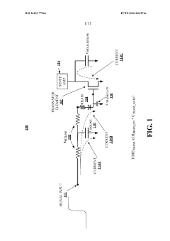
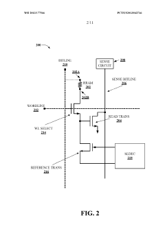
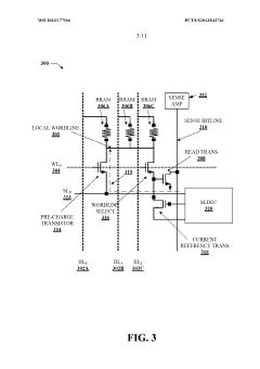
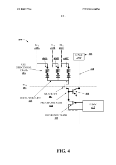
- The development of a high-speed RRAM architecture that connects multiple RRAM devices to a single read transistor, utilizing a reference transistor to apply a bias voltage and mitigate off-current, and employing a sensing circuit to quickly detect changes in electrical characteristics, enabling fast programming, reading, and erasing operations while reducing the number of read transistors and associated circuitry.
Industry Standards and Compatibility Requirements
The integration of HBM memory and RRAM technologies in sensor data processing systems requires adherence to multiple industry standards that govern memory interfaces, data integrity, and system interoperability. JEDEC standards play a crucial role, with JESD235 defining HBM specifications including electrical characteristics, timing parameters, and physical interfaces. For RRAM implementations, emerging JEDEC standards such as JESD47 series provide guidelines for non-volatile memory characterization and testing methodologies.
Memory controller compatibility represents a critical consideration, as sensor data processing systems must support diverse memory architectures simultaneously. The Open Compute Project (OCP) memory specifications establish baseline requirements for high-bandwidth memory subsystems, while PCIe Gen4/Gen5 standards define the interconnect protocols necessary for efficient data transfer between processing units and memory hierarchies.
Power management standards significantly impact deployment feasibility in sensor applications. The Advanced Configuration and Power Interface (ACPI) specifications mandate power state management capabilities, particularly relevant for RRAM's non-volatile characteristics and HBM's high-performance operational modes. Energy efficiency requirements under IEEE 1621 standards influence memory selection criteria for battery-powered sensor networks.
Data integrity and error correction standards present unique challenges when combining HBM and RRAM technologies. ECC implementation must comply with JEDEC JESD89 standards while accommodating the different error characteristics of volatile and non-volatile memory types. The reliability standards defined in JEDEC JESD47F become particularly important for RRAM longevity in continuous sensor data logging applications.
Thermal management compliance follows JEDEC JESD51 thermal measurement standards, addressing the distinct thermal profiles of HBM stacks versus distributed RRAM arrays. System-level integration must meet electromagnetic compatibility requirements under FCC Part 15 and CE marking standards, ensuring reliable operation in diverse sensor deployment environments without interference issues.
Power Efficiency and Thermal Management Considerations
Power efficiency represents a critical differentiator between HBM memory and RRAM technologies in sensor data processing applications. HBM memory typically consumes 1.2-1.35V operating voltage with power consumption ranging from 15-25W per stack during active operations. The high-bandwidth architecture necessitates continuous power delivery to maintain data integrity and support rapid read/write cycles. In contrast, RRAM operates at significantly lower voltages, typically 1.8-3.3V for switching operations, with standby power consumption approaching near-zero levels due to its non-volatile nature.
The power consumption patterns differ substantially between these technologies during sensor data processing workloads. HBM exhibits relatively constant power draw regardless of data access frequency, making it less suitable for intermittent sensor applications where duty cycles vary dramatically. RRAM demonstrates superior power scaling characteristics, consuming power primarily during write operations while maintaining data without continuous power supply during idle periods.
Thermal management challenges vary significantly between HBM and RRAM implementations. HBM stacks generate substantial heat due to their high-density architecture and continuous operation, requiring sophisticated cooling solutions including heat spreaders, thermal interface materials, and active cooling systems. The vertical stacking design exacerbates thermal challenges, as heat dissipation becomes increasingly difficult in compact form factors typical of sensor processing systems.
RRAM technology exhibits superior thermal characteristics with lower heat generation during normal operations. The resistive switching mechanism produces minimal thermal output during read operations, with heat generation occurring primarily during write cycles. This thermal profile aligns well with sensor data processing patterns where write operations are typically less frequent than read operations.
Temperature sensitivity affects both technologies differently in sensor environments. HBM performance degrades at elevated temperatures, requiring thermal throttling mechanisms that can impact processing throughput. RRAM demonstrates better temperature stability across wider operating ranges, maintaining consistent performance characteristics in harsh sensor deployment environments where temperature control may be limited or unavailable.
Unlock deeper insights with PatSnap Eureka Quick Research — get a full tech report to explore trends and direct your research. Try now!
Generate Your Research Report Instantly with AI Agent
Supercharge your innovation with PatSnap Eureka AI Agent Platform!