

Compare Racetrack Memory vs eDRAM for New Chip Architectures
MAY 14, 20269 MIN READ
Generate Your Research Report Instantly with AI Agent
PatSnap Eureka helps you evaluate technical feasibility & market potential.
Racetrack Memory vs eDRAM Background and Objectives
The evolution of memory technologies has been driven by the relentless pursuit of higher performance, lower power consumption, and increased density in modern computing systems. Traditional memory hierarchies face significant challenges as semiconductor scaling approaches physical limits, creating urgent demands for innovative memory solutions that can bridge the performance gap between volatile and non-volatile storage.
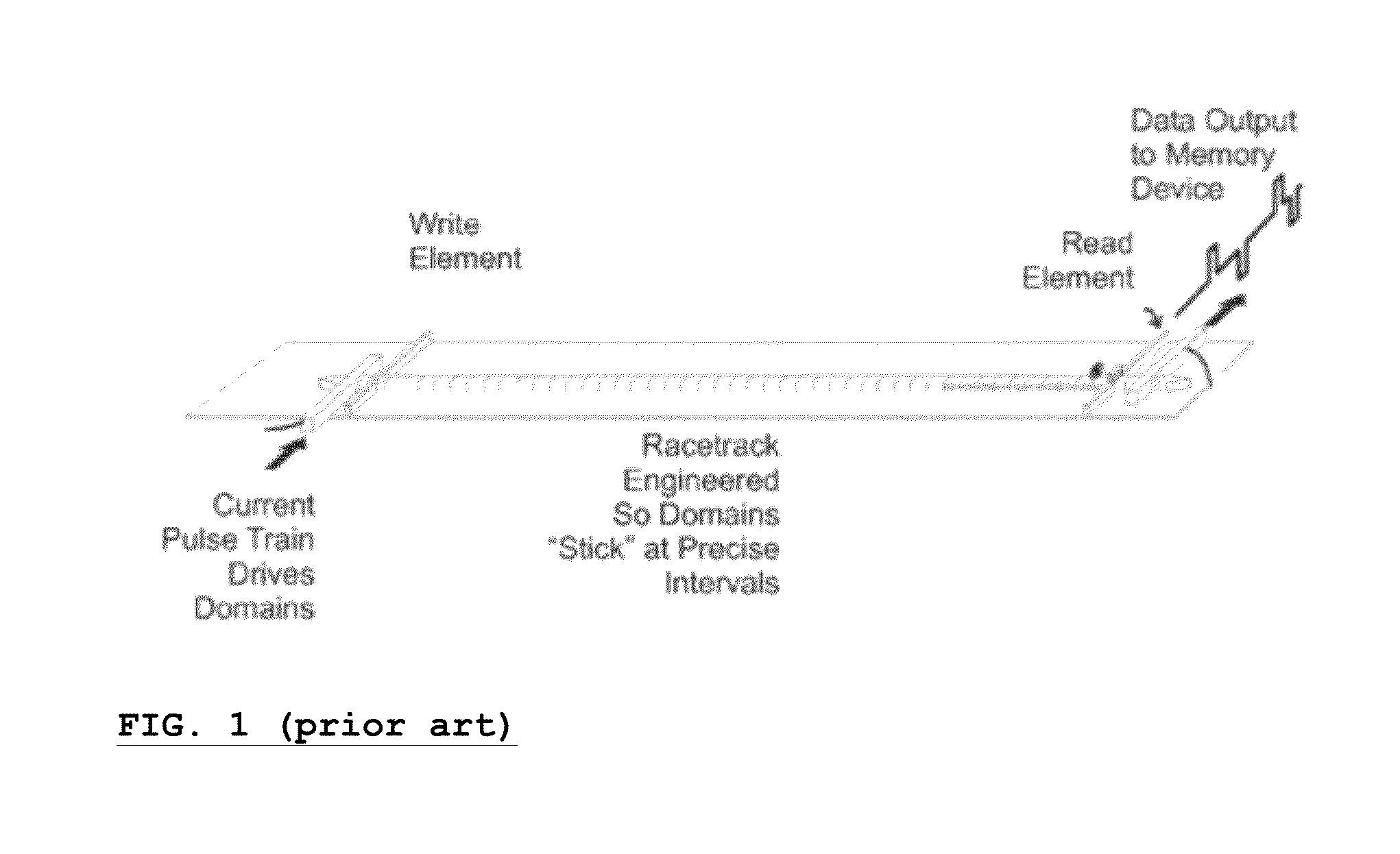
Racetrack memory represents a revolutionary approach to data storage, leveraging the principles of spintronics and magnetic domain wall motion. This technology, pioneered by IBM Research, utilizes nanoscale magnetic racetracks where data bits are stored as magnetic domains that can be shifted along the track using spin-polarized currents. The fundamental innovation lies in its ability to store multiple bits per device while maintaining non-volatility and potentially achieving near-SRAM access speeds.
Embedded Dynamic Random Access Memory (eDRAM) has emerged as a mature technology solution for addressing the memory wall problem in processor architectures. Unlike traditional DRAM, eDRAM can be integrated directly onto processor dies, offering significantly reduced latency and higher bandwidth. Major semiconductor manufacturers have successfully implemented eDRAM in various applications, from CPU caches to graphics processors, demonstrating its practical viability in commercial products.
The technological landscape has witnessed substantial progress in both memory paradigms over the past decade. Racetrack memory has evolved from theoretical concepts to functional prototypes, with researchers achieving significant milestones in domain wall velocity, retention characteristics, and fabrication processes. Meanwhile, eDRAM technology has matured through multiple generations, with improvements in cell design, refresh mechanisms, and integration density.
The primary objective of comparing these technologies centers on identifying optimal memory solutions for next-generation chip architectures. Key evaluation criteria include access latency, power efficiency, scalability potential, manufacturing complexity, and integration feasibility with existing semiconductor processes. This analysis aims to determine which technology offers superior advantages for specific application domains, ranging from high-performance computing to mobile processors.
Understanding the trade-offs between these memory technologies is crucial for strategic technology roadmap planning. The comparison seeks to establish clear performance benchmarks, identify potential hybrid implementation scenarios, and assess long-term viability in the context of emerging computing paradigms such as neuromorphic processors and quantum-classical hybrid systems.
Market Demand for Advanced Memory in New Chip Architectures
The semiconductor industry is experiencing unprecedented demand for advanced memory solutions as chip architectures evolve toward more complex, heterogeneous designs. Traditional memory hierarchies are increasingly inadequate for emerging applications that require both high performance and energy efficiency. This shift is driving substantial market interest in novel memory technologies that can bridge the gap between volatile and non-volatile storage while supporting diverse computational paradigms.
Artificial intelligence and machine learning workloads represent the most significant growth driver for advanced memory demand. These applications require memory systems capable of handling massive datasets with minimal latency while maintaining energy efficiency during intensive computational tasks. The proliferation of edge computing devices further amplifies this need, as these systems must balance performance requirements with strict power constraints in compact form factors.
Data center modernization initiatives are creating substantial demand for memory technologies that can support both traditional computing and emerging workloads. Cloud service providers are actively seeking memory solutions that can reduce total cost of ownership while improving system responsiveness. The growing adoption of in-memory computing and real-time analytics is pushing the boundaries of what conventional memory architectures can deliver effectively.
The automotive sector is emerging as a critical market segment, particularly with the advancement of autonomous driving systems and connected vehicle technologies. These applications demand memory solutions that combine high reliability with rapid access capabilities, creating opportunities for advanced memory technologies that can meet stringent automotive qualification standards while delivering superior performance characteristics.
Mobile and consumer electronics markets continue to drive demand for memory technologies that can support increasingly sophisticated applications while extending battery life. The integration of advanced camera systems, augmented reality capabilities, and always-on artificial intelligence features requires memory solutions that can efficiently handle diverse data types and access patterns without compromising device performance or user experience.
Enterprise computing environments are experiencing growing pressure to support hybrid workloads that combine traditional database operations with modern analytics and machine learning tasks. This convergence is creating demand for memory architectures that can adapt dynamically to varying computational requirements while maintaining consistent performance levels across different application types.
The Internet of Things ecosystem represents an emerging market segment where advanced memory technologies can enable new capabilities in resource-constrained environments. These applications require memory solutions that can operate efficiently across wide temperature ranges while supporting both frequent data updates and long-term information retention, characteristics that align well with emerging memory technology capabilities.
Current State and Challenges of Racetrack and eDRAM Technologies
Racetrack memory represents a revolutionary approach to non-volatile storage, leveraging magnetic domain walls that move along nanoscale tracks through spin-polarized currents. Current implementations demonstrate promising density advantages, with theoretical projections suggesting 100 times higher storage density compared to conventional DRAM. However, the technology faces significant challenges in achieving consistent domain wall motion control and maintaining data integrity during read/write operations. Manufacturing precision requirements at the nanoscale level present substantial fabrication hurdles, particularly in achieving uniform track dimensions and magnetic properties across large arrays.
eDRAM technology has matured considerably as an embedded memory solution, offering faster access times than traditional DRAM while maintaining reasonable power consumption levels. Leading semiconductor manufacturers have successfully integrated eDRAM into processor architectures, achieving access latencies in the range of 2-3 nanoseconds. The technology demonstrates excellent scalability for cache applications and intermediate storage layers in memory hierarchies. Nevertheless, eDRAM continues to struggle with refresh overhead requirements, typically needing refresh cycles every 64 milliseconds, which impacts overall system performance and power efficiency.
Manufacturing complexity represents a critical challenge for both technologies. Racetrack memory requires sophisticated lithography techniques to create precise magnetic tracks and control structures, with current yield rates remaining below commercial viability thresholds. Process variations significantly impact device performance, particularly affecting the current densities required for reliable domain wall manipulation. Temperature sensitivity further complicates deployment scenarios, as magnetic properties can drift under varying thermal conditions.
eDRAM faces integration challenges when embedded into advanced processor nodes, particularly regarding the additional mask layers and specialized capacitor structures required. The technology demands careful optimization of refresh algorithms to minimize performance penalties while ensuring data retention reliability. Power management becomes increasingly complex as eDRAM arrays scale, requiring sophisticated voltage regulation and timing control mechanisms.
Reliability concerns persist for both technologies in demanding computational environments. Racetrack memory exhibits susceptibility to magnetic field interference and requires robust error correction mechanisms to handle potential domain wall positioning errors. eDRAM reliability depends heavily on capacitor leakage characteristics, which vary significantly across process corners and operating conditions, necessitating adaptive refresh strategies and redundancy schemes for mission-critical applications.
Existing Memory Solutions for Next-Gen Chip Architectures
01 Racetrack memory architecture and domain wall motion
Racetrack memory utilizes magnetic domain walls that move along nanowires to store and access data. This technology leverages the controlled movement of magnetic domains through spin-polarized currents, enabling high-density storage with non-volatile characteristics. The architecture allows for sequential data access as domain walls shift positions along the track.- Racetrack memory architecture and domain wall motion: Racetrack memory utilizes magnetic domain walls that move along nanowires to store and access data. This technology leverages the controlled movement of magnetic domains through spin-polarized currents, enabling high-density storage with non-volatile characteristics. The architecture allows for sequential data access as domain walls shift positions along the track.
- eDRAM cell structure and capacitor design: Embedded dynamic random access memory features specialized capacitor structures integrated within logic processes. The technology focuses on maintaining charge storage capabilities while minimizing cell area and leakage currents. Various capacitor configurations and materials are employed to optimize retention time and reduce refresh requirements in embedded applications.
- Memory access speed and latency optimization: Both memory technologies implement different approaches to minimize access latency and maximize throughput. Advanced addressing schemes, prediction algorithms, and buffer management techniques are employed to reduce wait times and improve overall system performance. The optimization strategies vary significantly between the sequential nature of one technology and the random access capabilities of the other.
- Power consumption and retention mechanisms: Power efficiency differs substantially between these memory technologies, with one offering non-volatile storage eliminating standby power requirements, while the other requires periodic refresh operations to maintain data integrity. Various power management techniques, voltage scaling methods, and retention enhancement circuits are implemented to optimize energy consumption patterns.
- Manufacturing integration and scalability: The fabrication processes and integration challenges vary significantly between these memory technologies. One requires specialized magnetic materials and nanowire fabrication techniques, while the other focuses on capacitor integration within standard semiconductor processes. Scalability considerations include process compatibility, yield optimization, and cost-effectiveness for different application domains.
02 eDRAM cell structure and capacitor design
Embedded dynamic random access memory features specialized capacitor structures integrated within logic processes. The technology focuses on maintaining charge storage capabilities while minimizing cell area and leakage currents. Various capacitor configurations and materials are employed to optimize retention time and reduce refresh requirements.Expand Specific Solutions03 Power consumption and retention characteristics
The two memory technologies exhibit different power profiles and data retention behaviors. One technology offers non-volatile storage without continuous power requirements, while the other requires periodic refresh operations to maintain data integrity. Energy efficiency varies significantly between active and standby modes for each approach.Expand Specific Solutions04 Manufacturing integration and process compatibility
Integration approaches differ substantially between the two memory technologies regarding semiconductor fabrication processes. One technology requires specialized magnetic materials and nanofabrication techniques, while the other focuses on capacitor integration within standard logic processes. Process complexity and yield considerations impact manufacturing scalability.Expand Specific Solutions05 Performance characteristics and access methods
Access speed, latency, and throughput characteristics vary between the memory technologies based on their fundamental operating principles. Sequential versus random access patterns, read and write operation speeds, and scalability to different memory sizes present distinct advantages and limitations for each technology approach.Expand Specific Solutions
Key Players in Racetrack Memory and eDRAM Industry
The racetrack memory versus eDRAM comparison represents an emerging battleground in next-generation memory architectures, currently in the early development stage with limited commercial deployment. The market remains nascent with significant growth potential as data-intensive applications demand faster, more efficient memory solutions. Technology maturity varies considerably across players: established semiconductor giants like Intel, IBM, and TSMC leverage extensive R&D capabilities and manufacturing infrastructure to advance both technologies, while memory specialists such as Micron and Yangtze Memory focus on optimizing eDRAM implementations. Research institutions including Fudan University, Tsinghua University, and Max Planck Society contribute fundamental breakthroughs in racetrack memory physics and materials science. Companies like Qualcomm and Texas Instruments explore integration opportunities for mobile and embedded applications, though widespread adoption awaits resolution of manufacturing scalability and cost-effectiveness challenges inherent to both memory technologies.
Intel Corp.
Technical Solution: Intel has developed advanced eDRAM solutions integrated into their processor architectures, particularly for cache applications. Their eDRAM technology utilizes a single transistor and capacitor design with enhanced refresh mechanisms, providing higher density compared to SRAM while maintaining faster access times than conventional DRAM. Intel's approach focuses on embedding eDRAM directly into CPU dies using their advanced manufacturing processes, enabling large L4 cache implementations. The technology incorporates sophisticated error correction and refresh optimization algorithms to maintain data integrity while minimizing power overhead in mobile and server applications.
Strengths: Proven manufacturing capability with successful commercial deployment in processors, excellent density-performance balance. Weaknesses: Still requires periodic refresh operations and higher complexity compared to SRAM, limited to specific use cases.
International Business Machines Corp.
Technical Solution: IBM has been a pioneer in racetrack memory development, leveraging domain wall motion in magnetic nanowires for data storage. Their approach utilizes spin-transfer torque and spin-orbit torque mechanisms to move magnetic domains along nanowires, enabling non-volatile memory with DRAM-like performance. IBM's racetrack memory architecture features three-dimensional stacking capabilities, potentially achieving storage densities exceeding conventional memory technologies by orders of magnitude. The technology promises near-zero standby power consumption while maintaining fast read/write operations through controlled domain wall manipulation in ferromagnetic materials.
Strengths: Revolutionary non-volatile memory concept with ultra-high density potential and minimal power consumption. Weaknesses: Still in research phase with manufacturing complexity and reliability challenges for commercial deployment.
Core Patents in Racetrack Memory and eDRAM Innovation
Edram refresh apparatus and method
PatentActiveUS20200251161A1
Innovation
- A refresh controller is implemented to manage the refresh process by clocking the data bus at a higher rate than the given rate, reserving specific clock cycles for refresh operations, and prioritizing data entries based on their timeout values to ensure efficient bus utilization and minimize bandwidth constraints.


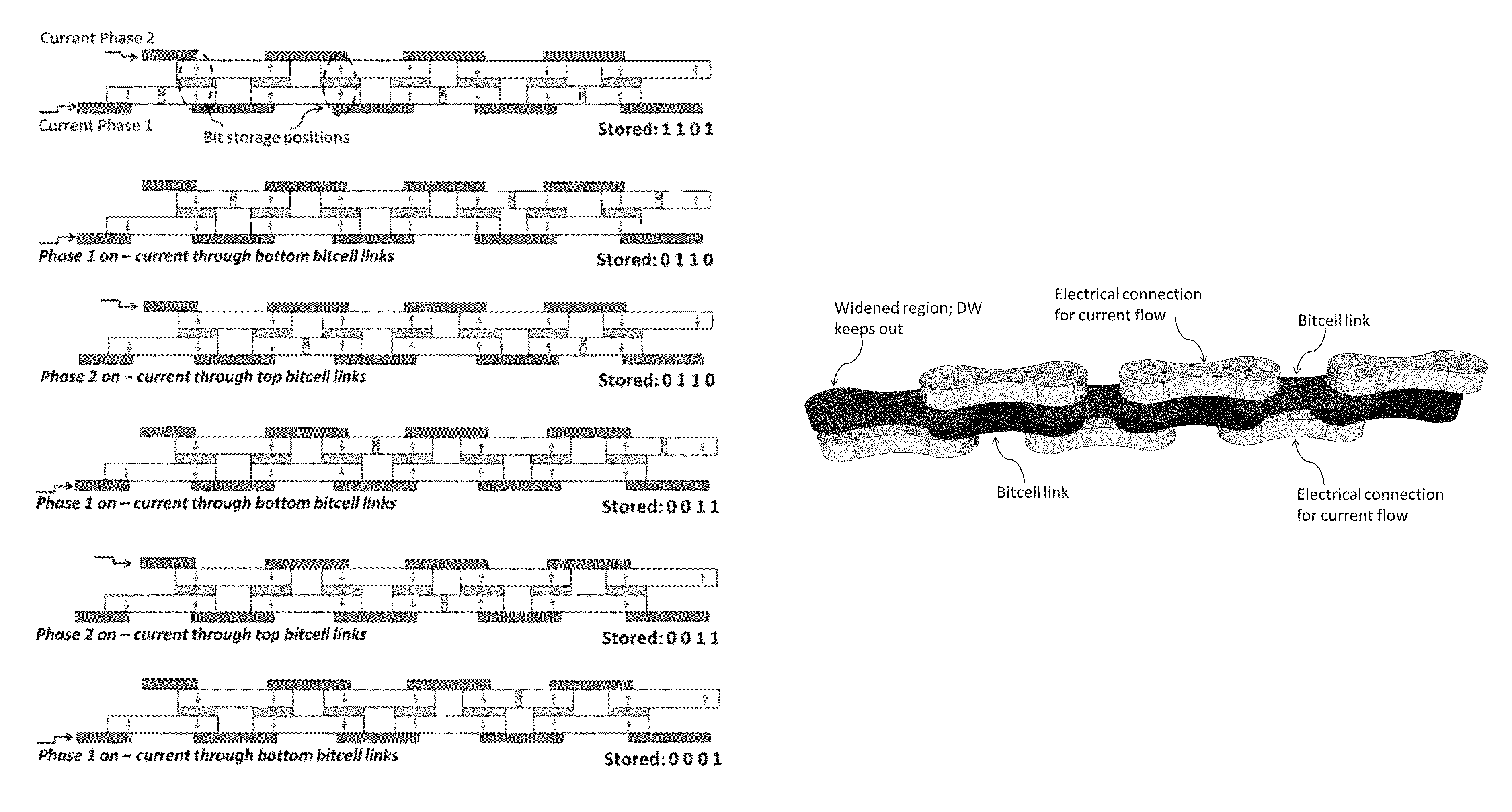
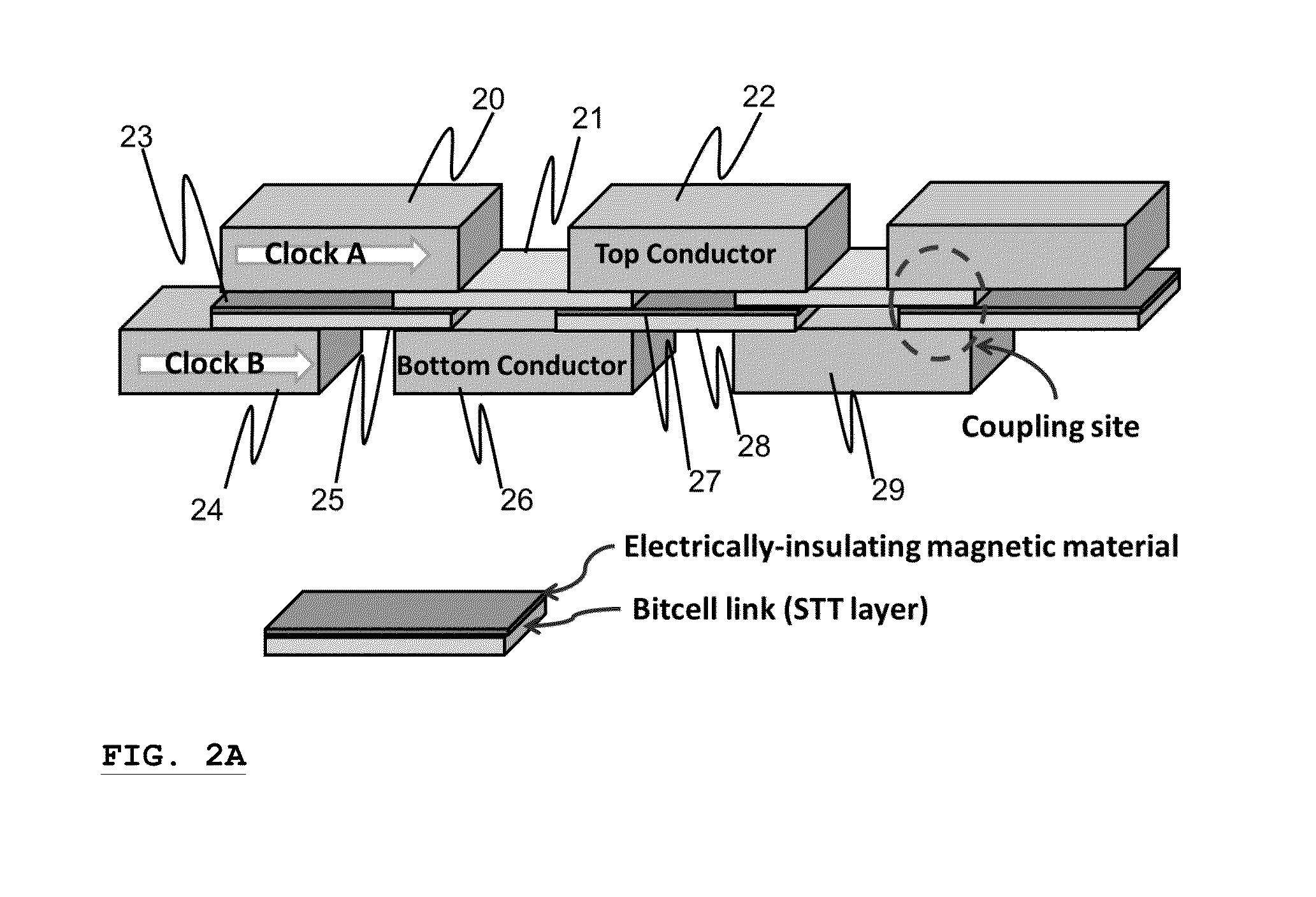
Chainlink memory
PatentInactiveUS9117523B1
Innovation
- The development of chainlink memory, where the racetrack is broken into magnetically coupled links, each handling one bit, with preferential pinning regions and unique current phases to prevent domain wall propagation and ensure data integrity, allowing for controlled bit propagation without annihilation.

Manufacturing Scalability and Cost Analysis
Manufacturing scalability represents a critical differentiator between Racetrack Memory and eDRAM technologies for next-generation chip architectures. Racetrack Memory demonstrates superior manufacturing scalability due to its simplified fabrication process, requiring fewer lithographic steps and specialized materials compared to eDRAM's complex capacitor structures. The technology leverages standard CMOS-compatible processes with magnetic materials that can be deposited using conventional sputtering techniques, enabling seamless integration into existing semiconductor fabrication facilities without substantial infrastructure modifications.
eDRAM manufacturing faces inherent scalability challenges as device dimensions shrink below 20nm nodes. The technology requires deep trench capacitors or metal-insulator-metal structures that demand precise aspect ratio control and specialized high-k dielectric materials. These requirements necessitate additional mask layers, increasing manufacturing complexity and reducing yield rates. Furthermore, eDRAM's refresh circuitry adds overhead to chip area utilization, impacting overall manufacturing efficiency.
Cost analysis reveals significant advantages for Racetrack Memory in high-volume production scenarios. The technology's planar structure eliminates expensive deep etching processes and reduces material waste during fabrication. Manufacturing costs scale favorably with volume due to simplified process flows and reduced dependency on exotic materials. Initial tooling investments remain moderate since existing semiconductor equipment can accommodate most Racetrack Memory processing requirements.
eDRAM cost structures reflect the technology's manufacturing complexity, with higher per-unit costs driven by additional processing steps and lower yield rates. The requirement for specialized capacitor formation techniques increases capital equipment needs and extends manufacturing cycle times. However, eDRAM benefits from mature supply chain ecosystems and established manufacturing expertise, potentially offsetting some cost disadvantages in near-term implementations.
Long-term cost projections favor Racetrack Memory as manufacturing volumes increase and process optimization reduces defect rates. The technology's inherent simplicity provides greater cost reduction potential through learning curve effects and process refinements. Conversely, eDRAM faces fundamental physical limitations that constrain further cost reductions, particularly as scaling approaches atomic dimensions and refresh power requirements become prohibitive for mobile applications.
Performance Benchmarking and Integration Strategies
Performance benchmarking between Racetrack Memory and eDRAM reveals distinct characteristics that significantly impact their suitability for emerging chip architectures. Racetrack Memory demonstrates superior read latency performance, typically achieving access times of 1-3 nanoseconds compared to eDRAM's 10-15 nanoseconds. However, write operations present a contrasting scenario, with Racetrack Memory requiring 5-10 nanoseconds due to domain wall manipulation, while eDRAM maintains consistent 10-15 nanosecond write cycles.
Energy consumption analysis shows Racetrack Memory's standby power advantage, consuming virtually zero static power due to its non-volatile nature. eDRAM requires continuous refresh operations consuming approximately 0.1-0.5 watts per gigabyte, making Racetrack Memory particularly attractive for battery-powered devices and data center applications where idle power consumption directly impacts operational costs.
Density benchmarks favor Racetrack Memory significantly, achieving theoretical densities of 20-50 times higher than eDRAM through its three-dimensional storage capability. This translates to potential integration of 100GB+ on-chip memory compared to eDRAM's current 2-4GB practical limits, fundamentally altering memory hierarchy design possibilities.
Integration strategies for Racetrack Memory require specialized fabrication processes incorporating magnetic materials and precise nanowire structures. Current integration approaches focus on hybrid architectures where Racetrack Memory serves as high-density storage cache while eDRAM handles high-frequency operations. This strategy leverages each technology's strengths while mitigating individual weaknesses.
eDRAM integration benefits from mature CMOS compatibility and established manufacturing processes. Its integration strategy emphasizes process node scaling and capacitor optimization techniques. Advanced integration methods include buried wordline architectures and high-k dielectric materials to maintain performance scaling.
Thermal management considerations differ substantially between technologies. Racetrack Memory generates localized heating during write operations due to current-induced domain wall motion, requiring targeted thermal design solutions. eDRAM exhibits more uniform thermal profiles but faces retention challenges at elevated temperatures, necessitating adaptive refresh rate management in high-performance applications.
Unlock deeper insights with PatSnap Eureka Quick Research — get a full tech report to explore trends and direct your research. Try now!
Generate Your Research Report Instantly with AI Agent
Supercharge your innovation with PatSnap Eureka AI Agent Platform!