

Comparing Racetrack Memory vs HBM3: Which Excels in Bandwidth?
MAY 14, 20269 MIN READ
Generate Your Research Report Instantly with AI Agent
PatSnap Eureka helps you evaluate technical feasibility & market potential.
Racetrack Memory vs HBM3 Technology Background and Bandwidth Goals
The evolution of memory technologies has been driven by the relentless demand for higher performance computing systems, particularly in data-intensive applications such as artificial intelligence, high-performance computing, and real-time analytics. Traditional memory architectures face fundamental limitations in meeting the exponentially growing bandwidth requirements of modern processors and accelerators.
Racetrack memory represents a revolutionary approach to data storage, leveraging the principles of spintronics and magnetic domain wall motion. This technology emerged from IBM Research in the early 2000s, building upon decades of magnetic storage research. The concept utilizes nanoscale magnetic tracks where data bits are stored as magnetic domains that can be shifted along the track using spin-polarized currents. This approach promises ultra-high density storage with non-volatile characteristics while potentially delivering exceptional access speeds.
High Bandwidth Memory 3 (HBM3) represents the latest iteration of 3D-stacked DRAM technology, evolving from the foundational work on through-silicon via (TSV) technology and advanced packaging techniques. HBM3 builds upon its predecessors by incorporating advanced manufacturing processes, improved thermal management, and optimized signal integrity designs. This technology addresses the memory wall problem by providing massive parallel data paths through its wide interface architecture.
The bandwidth performance goals for these technologies reflect different strategic approaches to memory system optimization. Racetrack memory aims to achieve bandwidth levels comparable to or exceeding current DRAM technologies while maintaining non-volatile storage characteristics. The target bandwidth specifications focus on leveraging the inherent parallelism of multiple racetrack structures operating simultaneously, potentially reaching hundreds of gigabytes per second per device.
HBM3 targets significantly higher bandwidth achievements through its proven 3D stacking methodology and wide interface design. Current specifications aim for bandwidth levels exceeding 800 GB/s per stack, representing substantial improvements over previous generations. The technology roadmap indicates potential for even higher bandwidth through increased stack heights, improved TSV density, and advanced signaling techniques.
The fundamental bandwidth optimization strategies differ significantly between these technologies. Racetrack memory focuses on eliminating traditional memory hierarchy bottlenecks by combining storage and memory functions, while HBM3 maximizes data throughput through massive parallelization and advanced packaging integration with processing units.
Market Demand Analysis for High-Bandwidth Memory Solutions
The global memory market is experiencing unprecedented demand driven by the exponential growth of data-intensive applications across multiple sectors. High-performance computing, artificial intelligence, machine learning, and advanced graphics processing require memory solutions that can deliver exceptional bandwidth to prevent bottlenecks in data processing pipelines. Traditional memory architectures are increasingly unable to meet the stringent performance requirements of modern computational workloads.
Data centers and cloud computing infrastructure represent the largest segment driving demand for high-bandwidth memory solutions. These facilities require memory systems capable of handling massive parallel processing tasks, real-time analytics, and complex algorithmic computations. The proliferation of edge computing and Internet of Things applications further amplifies the need for efficient memory architectures that can process data closer to its source while maintaining high throughput rates.
The gaming and entertainment industry constitutes another significant market segment demanding advanced memory solutions. Modern gaming applications, virtual reality systems, and high-resolution content creation tools require memory architectures that can support real-time rendering, complex physics simulations, and seamless user experiences. Professional graphics workstations and content creation platforms increasingly rely on memory systems that can handle large datasets and complex computational tasks simultaneously.
Automotive and autonomous vehicle development represents an emerging but rapidly growing market segment. Advanced driver assistance systems, autonomous navigation algorithms, and real-time sensor data processing require memory solutions that combine high bandwidth with low latency characteristics. The automotive industry's transition toward electric and autonomous vehicles creates substantial opportunities for innovative memory technologies that can support complex decision-making algorithms and sensor fusion applications.
Scientific research and simulation applications continue to drive demand for cutting-edge memory solutions. Climate modeling, pharmaceutical research, financial modeling, and engineering simulations require memory architectures capable of handling vast datasets while maintaining computational efficiency. Research institutions and government laboratories increasingly seek memory solutions that can accelerate scientific discovery through enhanced computational capabilities.
The telecommunications sector, particularly with the deployment of fifth-generation networks and beyond, creates additional demand for high-bandwidth memory solutions. Network infrastructure equipment, base stations, and communication processing systems require memory architectures that can handle increased data throughput and support advanced signal processing algorithms essential for modern communication networks.
Current State and Bandwidth Challenges in Memory Technologies
The contemporary memory technology landscape is characterized by an escalating demand for higher bandwidth capabilities, driven primarily by artificial intelligence workloads, high-performance computing applications, and data-intensive processing requirements. Traditional memory architectures are increasingly struggling to meet the bandwidth demands of modern processors, creating a significant performance bottleneck that limits system efficiency and computational throughput.
High Bandwidth Memory 3 (HBM3) represents the current pinnacle of conventional memory technology, delivering theoretical bandwidth capabilities of up to 819 GB/s per stack through its advanced 3D stacking architecture and wide I/O interface. HBM3 achieves this performance through sophisticated through-silicon via technology and parallel data channels, enabling simultaneous data transfer across multiple layers. However, this approach faces inherent physical limitations related to power consumption, thermal management, and manufacturing complexity that constrain further bandwidth scaling.
The primary bandwidth challenges in current memory technologies stem from the fundamental von Neumann architecture bottleneck, where data movement between processing units and memory storage creates latency and energy inefficiencies. Conventional DRAM-based solutions, including HBM variants, require constant refresh cycles that consume both power and bandwidth resources, while their charge-based storage mechanism introduces access latency that becomes increasingly problematic at higher operating frequencies.
Emerging non-volatile memory technologies are being explored as potential solutions to these bandwidth limitations. Racetrack memory, based on magnetic domain wall motion in nanowires, presents a fundamentally different approach to data storage and retrieval that could potentially overcome traditional bandwidth constraints. This technology leverages the movement of magnetic domains along specially designed nanowire tracks, enabling high-density storage with potentially superior bandwidth characteristics compared to charge-based memory systems.
The bandwidth challenge is further complicated by the growing disparity between processor performance improvements and memory access speeds, commonly referred to as the memory wall problem. While processor capabilities continue to advance rapidly, memory bandwidth improvements have been more incremental, creating an increasingly significant performance gap that affects overall system efficiency and limits the potential of next-generation computing applications.
Current memory technologies also face scalability challenges as they approach physical limits of miniaturization and power efficiency. The industry requires breakthrough innovations that can deliver substantially higher bandwidth while maintaining energy efficiency and cost-effectiveness for widespread adoption across various computing platforms and applications.
Current Bandwidth Solutions in Racetrack and HBM3
01 Racetrack memory architecture and domain wall manipulation
Racetrack memory utilizes magnetic domain walls that can be moved along nanowires through spin-polarized currents. This technology enables high-density data storage by storing multiple bits in a single nanowire track. The manipulation of domain walls allows for sequential access to stored data bits, providing a novel approach to non-volatile memory storage with potential for high storage density and low power consumption.- Racetrack memory architecture and domain wall manipulation: Racetrack memory utilizes magnetic domain walls that can be moved along nanowires through spin-polarized currents. This technology enables high-density data storage by positioning multiple bits along a single track. The manipulation of domain walls through current injection allows for non-volatile memory operations with potentially lower power consumption compared to traditional memory technologies.
- High bandwidth memory interface optimization: Advanced memory interfaces are designed to maximize data throughput through improved signaling techniques, parallel data paths, and optimized timing protocols. These interfaces support higher frequencies and wider data buses to achieve increased bandwidth performance. Error correction and signal integrity mechanisms are integrated to maintain reliability at high speeds.
- Memory controller and access scheduling: Sophisticated memory controllers manage data flow between processors and memory arrays through intelligent scheduling algorithms. These controllers optimize memory access patterns, reduce latency, and maximize bandwidth utilization. Advanced queuing mechanisms and predictive algorithms help coordinate multiple memory requests efficiently.
- Three-dimensional memory stacking and integration: Three-dimensional memory architectures enable higher density storage through vertical stacking of memory layers. This approach increases capacity while maintaining a smaller footprint and can improve bandwidth through parallel access to multiple layers. Advanced manufacturing techniques and through-silicon vias enable efficient interconnection between stacked memory elements.
- Power management and thermal optimization: Advanced power management techniques reduce energy consumption in high-performance memory systems while maintaining optimal operating temperatures. Dynamic voltage and frequency scaling, along with selective activation of memory banks, help balance performance and power efficiency. Thermal management solutions ensure reliable operation under high bandwidth conditions.
02 High bandwidth memory interface optimization
Advanced memory interfaces are designed to maximize data transfer rates through optimized signaling protocols and multi-channel architectures. These implementations focus on reducing latency and increasing throughput by employing sophisticated timing control mechanisms, parallel data paths, and enhanced signal integrity techniques to achieve superior bandwidth performance in high-speed memory systems.Expand Specific Solutions03 Memory controller and bandwidth management
Memory controllers implement advanced algorithms for managing data flow and optimizing bandwidth utilization across multiple memory channels. These systems incorporate intelligent scheduling mechanisms, buffer management strategies, and adaptive control techniques to ensure efficient data transfer while minimizing conflicts and maximizing overall system performance in high-bandwidth memory applications.Expand Specific Solutions04 Three-dimensional memory structures and stacking
Three-dimensional memory architectures enable increased storage density through vertical stacking of memory cells and interconnect layers. These structures utilize advanced fabrication techniques to create multi-layer memory arrays that can significantly enhance storage capacity while maintaining compact form factors. The vertical integration approach allows for improved bandwidth through parallel access to multiple memory layers.Expand Specific Solutions05 Signal processing and data integrity in high-speed memory
High-speed memory systems require sophisticated signal processing techniques to maintain data integrity at elevated operating frequencies. These implementations include error correction mechanisms, signal conditioning circuits, and advanced modulation schemes that ensure reliable data transmission across high-bandwidth memory interfaces while compensating for signal degradation and noise effects.Expand Specific Solutions
Major Players in Racetrack Memory and HBM3 Development
The bandwidth comparison between Racetrack Memory and HBM3 represents an emerging competitive landscape in the advanced memory technology sector. The industry is currently in a transitional phase, with HBM3 representing mature high-bandwidth memory solutions while Racetrack Memory remains in early research and development stages. Market dynamics are dominated by established players like Samsung Electronics, Micron Technology, and ChangXin Memory Technologies who lead HBM3 production, alongside emerging Chinese manufacturers such as Yangtze Memory Technologies and Xi'an Sinochip Semiconductors. Technology maturity varies significantly, with companies like Intel, AMD, and Taiwan Semiconductor Manufacturing providing foundational support for HBM3 implementation, while research institutions including Zhejiang University and University of Electronic Science & Technology of China explore Racetrack Memory's potential. The competitive advantage currently favors HBM3's proven bandwidth capabilities, though Racetrack Memory's theoretical performance benefits continue attracting investment from companies like Google and specialized firms such as AvicenaTech Corp for next-generation interconnect solutions.
Samsung Electronics Co., Ltd.
Technical Solution: Samsung has developed advanced HBM3 memory solutions achieving bandwidth up to 819 GB/s per stack with 24GB capacity. Their HBM3 technology utilizes through-silicon via (TSV) technology and advanced packaging techniques to achieve high-density stacking of DRAM dies. Samsung's HBM3 features improved power efficiency compared to previous generations while maintaining exceptional bandwidth performance. The company has also invested in research for next-generation memory technologies including exploration of racetrack memory concepts, though their primary focus remains on commercializing HBM3 for AI accelerators and high-performance computing applications.
Strengths: Market leader in HBM3 production with proven high bandwidth performance and established manufacturing capabilities. Weaknesses: Limited commercial development in racetrack memory technology compared to traditional memory solutions.
Micron Technology, Inc.
Technical Solution: Micron has developed HBM3 memory solutions delivering up to 665 GB/s bandwidth per stack with enhanced power efficiency. Their approach focuses on optimizing the memory controller interface and implementing advanced signal integrity techniques to maximize data transfer rates. Micron's HBM3 products feature improved thermal management and reduced latency compared to HBM2E. The company has also conducted research into emerging memory technologies including domain wall-based memories similar to racetrack concepts, exploring their potential for future high-bandwidth applications in data centers and AI workloads.
Strengths: Strong HBM3 manufacturing capabilities with competitive bandwidth performance and thermal optimization. Weaknesses: Early-stage research in racetrack memory technology with no commercial products announced.
Core Patents in High-Bandwidth Memory Innovation
Tccd specification for scaling bandwidth on high bandwidth memory devices and associated systems and methods
PatentPendingUS20250356904A1
Innovation
- Implementing a 4N architecture with increased bank groups per channel, extending tCCDL CLK cycle periods, introducing a new timing parameter tCCDS_SID for commands to different bank groups in the same stack, and optimizing transmit/receive circuits to maintain synchronization and saturation of the DQ bus.


Optically interconnected high bandwidth memory architectures
PatentWO2024215908A1
Innovation
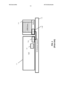
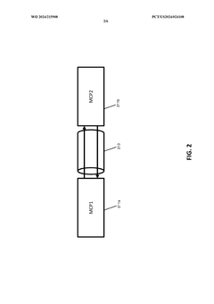
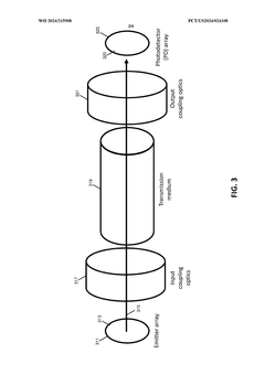
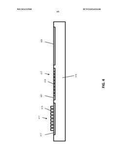
- The implementation of optically interconnected high bandwidth memory architectures using multi-chip packages with optical interfaces and transmission media, such as optical fibers, to enable longer interconnects between System-on-Chip (SoC) and HBM, allowing for increased memory capacity and reduced thermal stress by physically separating HBM from the hot SoC.
Manufacturing Scalability and Cost Analysis
Manufacturing scalability represents a critical differentiator between Racetrack Memory and HBM3 technologies, with each facing distinct challenges in mass production. HBM3 leverages established semiconductor manufacturing processes, utilizing proven through-silicon via (TSV) technology and advanced packaging techniques that have been refined through multiple generations of high bandwidth memory products. The manufacturing infrastructure for HBM3 builds upon existing DRAM fabrication capabilities, requiring modifications primarily in the stacking and interconnect processes rather than fundamental changes to production lines.
Racetrack Memory faces significantly greater manufacturing complexity due to its reliance on precise magnetic domain manipulation and nanowire fabrication. The technology requires specialized equipment for creating uniform magnetic nanowires with consistent properties across wafer scales. Current manufacturing processes struggle with maintaining the precise magnetic characteristics necessary for reliable domain wall movement, leading to yield challenges that directly impact scalability potential.
Cost analysis reveals substantial differences in production economics between the two technologies. HBM3 benefits from economies of scale within the established DRAM manufacturing ecosystem, where foundries can leverage existing equipment investments and supply chain relationships. The primary cost drivers include advanced packaging processes and the complexity of multi-die stacking, but these are offset by mature manufacturing processes and high-volume production capabilities.
Racetrack Memory currently exhibits higher per-unit manufacturing costs due to specialized fabrication requirements and lower production volumes. The technology demands precise control over magnetic properties, requiring additional process steps and quality control measures that increase manufacturing complexity. However, the potential for higher storage density could eventually provide cost advantages in terms of cost-per-bit metrics.
Long-term scalability projections favor different aspects of each technology. HBM3 can achieve near-term scalability improvements through enhanced stacking techniques and process node advancement, but faces physical limitations in vertical integration. Racetrack Memory offers superior theoretical scalability potential through three-dimensional storage architectures, though achieving manufacturing maturity requires significant technological breakthroughs in magnetic domain control and fabrication precision.
Power Efficiency Comparison in Bandwidth Performance
Power efficiency represents a critical differentiator between Racetrack Memory and HBM3 when evaluating their bandwidth performance capabilities. The fundamental architectural differences between these technologies create distinct power consumption profiles that directly impact their practical deployment scenarios.
Racetrack Memory demonstrates superior power efficiency through its innovative magnetic domain wall manipulation mechanism. The technology operates by shifting magnetic domains along nanowires using spin-polarized currents, requiring significantly lower power compared to traditional charge-based storage systems. During high-bandwidth operations, Racetrack Memory maintains relatively stable power consumption regardless of access frequency, as the domain wall movement process inherently consumes minimal energy per bit transferred.
HBM3, while delivering exceptional bandwidth performance, exhibits higher power consumption due to its DRAM-based architecture and complex through-silicon via interconnects. The technology requires continuous refresh operations to maintain data integrity, contributing to baseline power consumption even during idle states. Additionally, the high-speed signaling required for achieving peak bandwidth performance of up to 819 GB/s necessitates substantial power investment in driver circuits and signal conditioning.
The power-to-bandwidth ratio analysis reveals Racetrack Memory's advantage in sustained workloads. While HBM3 can achieve higher absolute bandwidth figures, its power consumption scales proportionally with performance demands. Racetrack Memory maintains more consistent power efficiency across varying bandwidth utilization levels, making it particularly attractive for battery-powered devices and data center applications where thermal management is crucial.
Temperature sensitivity further distinguishes these technologies' power efficiency characteristics. HBM3's performance and power consumption are significantly affected by thermal conditions, requiring additional cooling infrastructure that increases overall system power requirements. Racetrack Memory exhibits greater thermal stability, maintaining power efficiency across broader temperature ranges without requiring extensive thermal management solutions.
The standby power consumption comparison heavily favors Racetrack Memory, as its non-volatile nature eliminates the need for continuous refresh operations. This characteristic becomes increasingly important in mobile and edge computing applications where power efficiency during low-activity periods directly impacts battery life and operational costs.
Unlock deeper insights with PatSnap Eureka Quick Research — get a full tech report to explore trends and direct your research. Try now!
Generate Your Research Report Instantly with AI Agent
Supercharge your innovation with PatSnap Eureka AI Agent Platform!