

How to Increase Racetrack Memory's Yield Using Advanced Lithography
MAY 14, 20269 MIN READ
Generate Your Research Report Instantly with AI Agent
Patsnap Eureka helps you evaluate technical feasibility & market potential.
Racetrack Memory Lithography Background and Objectives
Racetrack memory represents a revolutionary approach to data storage that leverages the magnetic properties of domain walls in ferromagnetic nanowires. This technology, first conceptualized by IBM Research in 2008, fundamentally differs from conventional memory architectures by utilizing current-driven domain wall motion to shift magnetic bits along a nanoscale track. The concept draws inspiration from early magnetic bubble memory but employs modern spintronics principles to achieve unprecedented storage density and energy efficiency.
The evolution of racetrack memory has been intrinsically linked to advances in nanofabrication techniques. Early prototypes relied on electron beam lithography to create proof-of-concept devices, but the transition to practical applications demands manufacturing processes capable of producing billions of nanowires with precise dimensional control. The critical dimensions required for functional racetrack devices typically range from 10 to 100 nanometers in width, with length-to-width aspect ratios exceeding 100:1 in many designs.
Current lithographic challenges in racetrack memory fabrication stem from the stringent requirements for dimensional uniformity and defect minimization. Variations in nanowire width directly impact domain wall pinning behavior and current thresholds for magnetic switching, leading to device-to-device performance variations that reduce overall yield. Edge roughness, a common artifact of lithographic patterning, creates unintended pinning sites that can trap domain walls and cause operational failures.
The primary objective of integrating advanced lithography techniques is to achieve manufacturing yields exceeding 95% for racetrack memory arrays containing millions of individual devices. This target necessitates reducing critical dimension variations to less than 5% across entire wafers while simultaneously minimizing line edge roughness to below 2 nanometers RMS. Additionally, the lithographic process must maintain compatibility with the complex material stack required for racetrack devices, including ferromagnetic layers, tunnel barriers, and contact metallization.
Advanced lithographic approaches under investigation include extreme ultraviolet lithography for high-resolution patterning, directed self-assembly for achieving sub-10nm features, and multi-patterning techniques for enhanced dimensional control. These methods aim to overcome the fundamental limitations of conventional optical lithography while providing the throughput necessary for commercial viability. The successful implementation of these techniques will enable racetrack memory to achieve its theoretical storage density advantages while maintaining the reliability standards required for enterprise storage applications.
Market Demand for High-Density Magnetic Memory Solutions
The global magnetic memory market is experiencing unprecedented growth driven by the exponential increase in data generation and storage requirements across multiple industries. Enterprise data centers, cloud computing infrastructure, and edge computing applications are demanding memory solutions that can deliver both high density and exceptional performance while maintaining energy efficiency. Traditional memory technologies are approaching their physical scaling limits, creating substantial market opportunities for next-generation solutions like racetrack memory.
Data-intensive applications including artificial intelligence, machine learning, and real-time analytics are particularly driving demand for high-density magnetic memory solutions. These applications require memory architectures capable of handling massive datasets with minimal latency while providing non-volatile storage characteristics. The automotive industry's transition toward autonomous vehicles and advanced driver assistance systems further amplifies this demand, as these systems generate and process enormous amounts of sensor data requiring immediate access and long-term retention.
The Internet of Things ecosystem represents another significant market driver, with billions of connected devices requiring efficient memory solutions that can operate reliably in diverse environmental conditions. Edge computing deployments specifically need memory technologies that combine high density with low power consumption, making magnetic memory solutions increasingly attractive compared to conventional alternatives.
Market research indicates strong demand from hyperscale data center operators seeking to optimize their storage hierarchies. These organizations are actively evaluating emerging memory technologies that can bridge the performance gap between volatile and non-volatile storage while reducing overall system complexity and operational costs. The ability to achieve higher storage densities directly translates to reduced physical footprint and improved total cost of ownership.
Manufacturing yield improvements through advanced lithography techniques directly address market concerns about cost-effectiveness and commercial viability. Higher yields enable more competitive pricing structures, making high-density magnetic memory solutions accessible to broader market segments beyond premium applications. This cost reduction potential is particularly crucial for consumer electronics manufacturers who require high-performance memory solutions at scale.
The telecommunications industry's 5G infrastructure rollout is creating additional demand for high-density memory solutions capable of supporting ultra-low latency applications and massive data throughput requirements. Network equipment manufacturers are seeking memory technologies that can maintain performance consistency while operating in challenging deployment environments.
Current Lithography Limitations in Racetrack Memory Fabrication
Racetrack memory fabrication faces significant lithographic challenges that directly impact device yield and commercial viability. The fundamental limitation stems from the need to create extremely narrow magnetic nanowires with widths typically ranging from 10 to 50 nanometers, which pushes current lithography systems to their resolution limits. Traditional photolithography techniques struggle to achieve the required dimensional control and uniformity across large wafer areas, resulting in substantial variations in nanowire geometry that compromise device performance.
Critical dimensional control represents one of the most pressing challenges in racetrack memory manufacturing. The magnetic domain walls that store information in racetrack devices are highly sensitive to nanowire width variations, with even minor deviations of 2-3 nanometers potentially causing domain wall pinning or unpredictable motion dynamics. Current 193nm immersion lithography systems, while mature and widely deployed, cannot consistently achieve the sub-20nm features required for high-density racetrack arrays without multiple patterning techniques that introduce additional complexity and potential defect sources.
Edge roughness and sidewall quality present another major fabrication hurdle. Racetrack memory performance depends critically on smooth nanowire edges to ensure predictable domain wall propagation. Line edge roughness values exceeding 2-3 nanometers can create pinning sites that trap domain walls, leading to write/read failures and reduced device reliability. Conventional lithography processes often produce sidewall angles and surface roughness that fall short of the stringent requirements for optimal racetrack operation.
Pattern fidelity across large arrays poses scalability challenges for commercial production. Racetrack memory devices require thousands of parallel nanowires arranged in dense arrays, demanding exceptional uniformity in critical dimensions, pitch accuracy, and overlay precision. Current lithography systems exhibit systematic and random variations that become more pronounced as feature sizes decrease, resulting in yield losses that increase exponentially with array size.
Defect density and pattern collapse issues further limit manufacturing yield. The high aspect ratio structures required for vertical racetrack implementations are particularly susceptible to pattern collapse during development and etching processes. Additionally, particle contamination and mask defects become increasingly problematic as feature sizes approach the wavelength limits of existing lithography tools, creating systematic yield detractors that challenge economic viability.
Existing Advanced Lithography Solutions for Memory Yield
01 Manufacturing process optimization for racetrack memory devices
Various manufacturing techniques and process optimizations are employed to improve the yield of racetrack memory devices. These include advanced lithography methods, precise material deposition techniques, and controlled annealing processes that enhance the structural integrity and performance characteristics of the magnetic nanowires used in racetrack memory systems.- Manufacturing process optimization for racetrack memory devices: Various manufacturing techniques and process optimizations are employed to improve the yield of racetrack memory devices during fabrication. These methods focus on controlling material deposition, etching processes, and structural formation to minimize defects and enhance device reliability. Process parameters such as temperature control, timing sequences, and material purity are critical factors in achieving higher manufacturing yields.
- Defect detection and correction mechanisms: Implementation of defect detection systems and error correction mechanisms to identify and compensate for manufacturing defects in racetrack memory arrays. These systems can detect faulty memory cells, domain wall movement irregularities, and other structural defects that may occur during production. Advanced testing methodologies and built-in self-test circuits are utilized to screen devices and improve overall yield rates.
- Material composition and structure optimization: Optimization of magnetic materials, substrate compositions, and multilayer structures to enhance the performance and manufacturability of racetrack memory devices. This includes the selection of appropriate ferromagnetic materials, barrier layers, and contact materials that provide stable magnetic properties while maintaining high fabrication yields. Material engineering approaches focus on reducing interface defects and improving magnetic domain stability.
- Circuit design and layout strategies for yield improvement: Development of circuit architectures and layout designs that are more tolerant to manufacturing variations and defects. These strategies include redundancy schemes, adaptive circuit configurations, and design rules that minimize the impact of process variations on device functionality. Layout optimization techniques help reduce critical dimension sensitivity and improve overall manufacturing success rates.
- Testing and characterization methods for yield assessment: Advanced testing methodologies and characterization techniques specifically designed to evaluate racetrack memory device performance and identify yield-limiting factors. These methods include electrical testing protocols, magnetic characterization techniques, and statistical analysis approaches to assess device functionality and reliability. Comprehensive testing strategies enable better understanding of failure modes and guide process improvements.
02 Defect detection and quality control methods
Implementation of sophisticated defect detection systems and quality control methodologies to identify and minimize manufacturing defects that could impact racetrack memory yield. These approaches include real-time monitoring during fabrication, post-processing inspection techniques, and statistical analysis methods to ensure consistent device performance and reliability.Expand Specific Solutions03 Material composition and structure optimization
Development of optimized material compositions and structural configurations for magnetic domain walls and nanowire architectures that enhance device yield. This includes the selection of appropriate magnetic materials, substrate materials, and interface engineering to minimize defects and improve the uniformity of magnetic properties across the device array.Expand Specific Solutions04 Testing and characterization methodologies
Advanced testing protocols and characterization techniques specifically designed for evaluating racetrack memory device performance and yield metrics. These methods enable comprehensive assessment of device functionality, identification of failure modes, and optimization of manufacturing parameters to achieve higher production yields.Expand Specific Solutions05 Design optimization for improved manufacturability
Strategic design modifications and layout optimizations that enhance the manufacturability and yield of racetrack memory arrays. This includes considerations for device scaling, interconnect design, thermal management, and integration with complementary circuit elements to ensure robust and high-yield production processes.Expand Specific Solutions
Key Players in Racetrack Memory and Lithography Industry
The racetrack memory technology landscape is in its early development stage, characterized by significant research investments but limited commercial deployment. The market remains nascent with substantial growth potential as the technology addresses critical memory performance bottlenecks in computing systems. Technology maturity varies significantly across key players, with established semiconductor giants like IBM, Samsung Electronics, and Infineon Technologies leading fundamental research and patent development. Memory specialists including Yangtze Memory Technologies and ChangXin Memory Technologies are exploring integration pathways, while academic institutions such as Max Planck Gesellschaft and Xiamen University contribute theoretical breakthroughs. The competitive environment reflects a research-intensive phase where advanced lithography solutions for yield improvement represent a critical technological barrier requiring collaboration between equipment manufacturers, foundries, and research organizations to achieve commercial viability.
International Business Machines Corp.
Technical Solution: IBM has developed comprehensive racetrack memory solutions utilizing advanced lithography techniques including extreme ultraviolet (EUV) lithography for precise nanowire fabrication. Their approach focuses on optimizing domain wall motion control through improved material engineering and lithographic patterning. IBM's technology incorporates sophisticated error correction algorithms and yield enhancement methodologies, including advanced process control systems that monitor critical dimensions during fabrication. They have demonstrated successful integration of racetrack memory with CMOS technology using 7nm and 5nm process nodes, achieving significant improvements in storage density and operational reliability through precise lithographic control of magnetic nanowire structures.
Strengths: Pioneer in racetrack memory research with extensive patent portfolio and proven CMOS integration capabilities. Advanced EUV lithography expertise enables precise nanoscale fabrication. Weaknesses: High development costs and complex manufacturing processes may limit commercial scalability in near term.
Samsung Electronics Co., Ltd.
Technical Solution: Samsung has developed advanced racetrack memory fabrication processes leveraging their leading-edge semiconductor manufacturing capabilities. Their approach utilizes state-of-the-art EUV lithography systems combined with advanced materials engineering to achieve high-yield production of magnetic nanowires. Samsung's technology focuses on optimizing the lithographic process parameters, including exposure dose control, resist chemistry, and etching processes to minimize defects in racetrack structures. They have implemented comprehensive process monitoring and control systems that enable real-time adjustment of lithographic parameters to maintain consistent device performance across wafer-scale production. Their solution integrates advanced metrology tools for in-line defect detection and yield optimization.
Strengths: World-class semiconductor manufacturing infrastructure with proven high-volume production capabilities. Advanced EUV lithography and process control expertise. Weaknesses: Focus primarily on memory applications may limit exploration of novel racetrack architectures for specialized computing applications.
Core Lithography Innovations for Racetrack Memory Yield
In-situ design method and system for improved memory yield
PatentInactiveUS8170857B2
Innovation
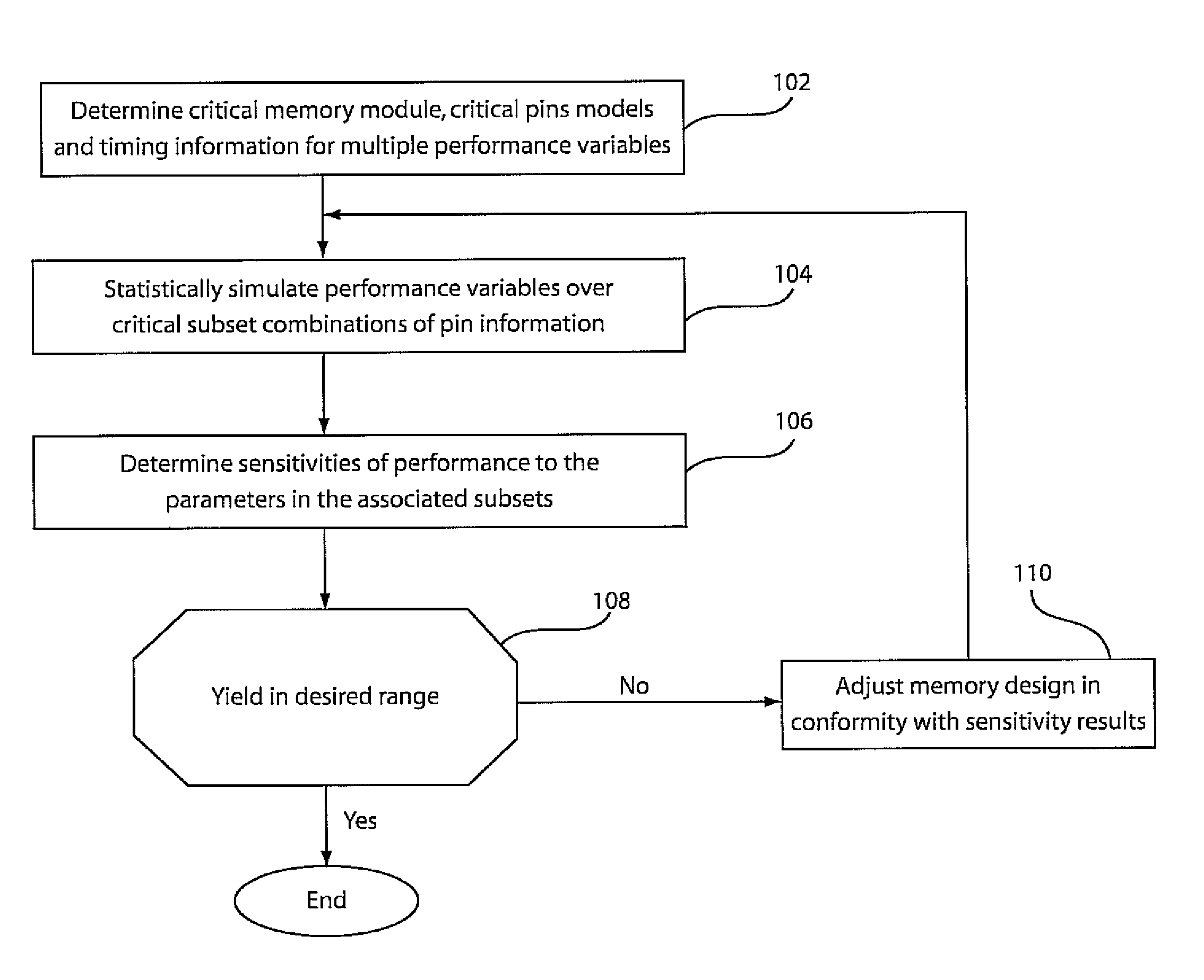
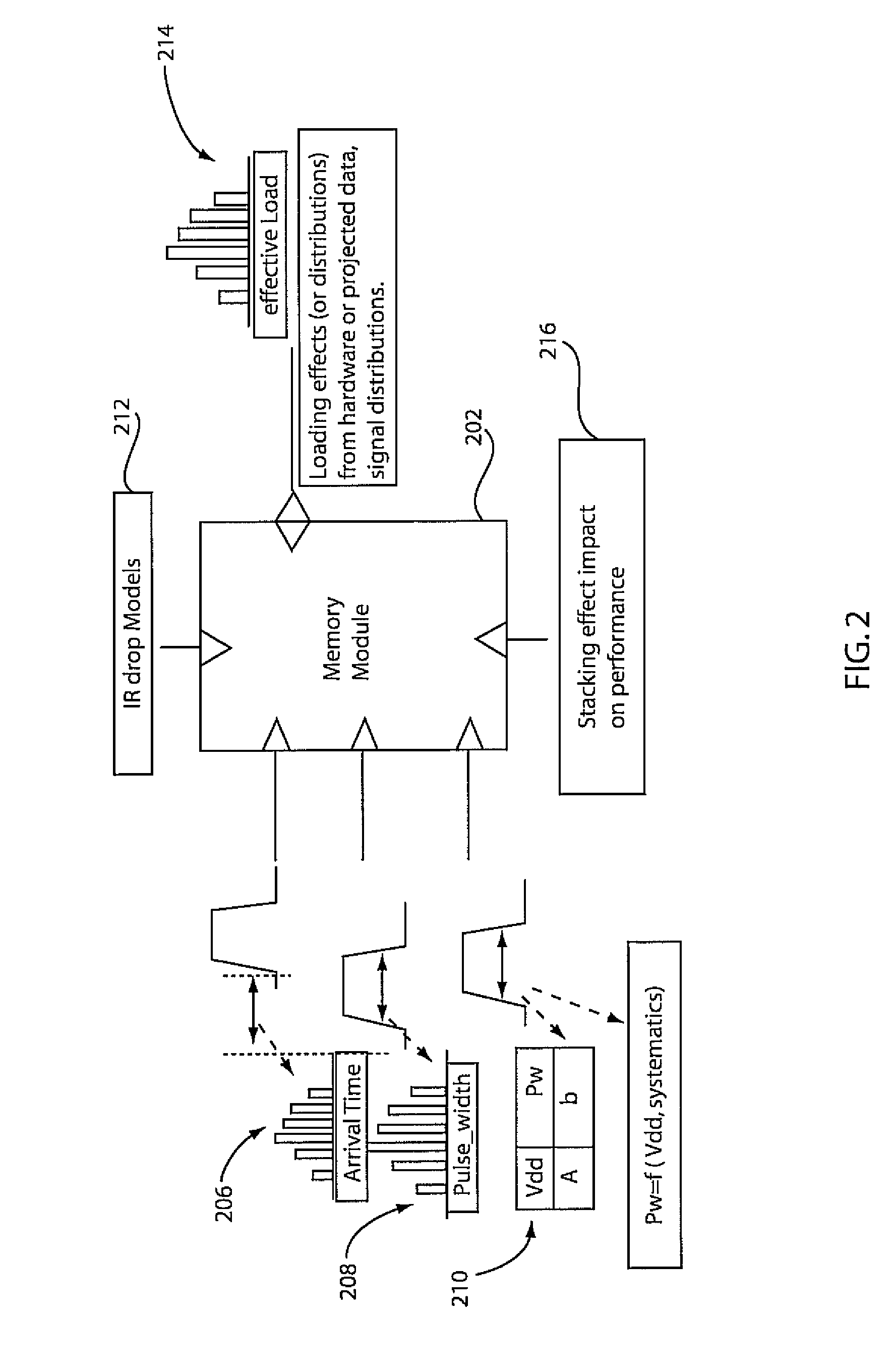
- A system and method that determines target memory module performance variables, statistically simulates pin information combinations, and adjusts design sensitivities to optimize yield, using fast statistical analysis techniques and small module abstractions to capture timing and loading information, enabling more accurate yield estimation and improving memory performance.

Race-track memory with improved domain wall motion control
PatentActiveKR1020220029347A
Innovation
- A race track memory layer with interleaved bit positions and domain wall traps, featuring distinct domain wall velocities and Dzyaloshinskii-Moriya Interaction (DMI) and Synthetic Antiferromagnetic (SAF) effects, along with a nonmagnetic coupling layer and ferromagnetic layer, to modulate domain wall speeds and improve control.


Semiconductor Manufacturing Standards and Regulations
The semiconductor manufacturing industry operates under a comprehensive framework of international and regional standards that directly impact racetrack memory production and yield optimization. The International Semiconductor Equipment and Materials International (SEMI) standards provide fundamental guidelines for advanced lithography processes, including specifications for extreme ultraviolet (EUV) lithography systems essential for achieving the nanoscale precision required in racetrack memory fabrication. These standards define critical parameters such as overlay accuracy, critical dimension uniformity, and defect density thresholds that manufacturers must meet to ensure acceptable yield rates.
Quality management systems in semiconductor manufacturing are governed by ISO 9001 and industry-specific standards like SEMI E10 for equipment reliability and SEMI F47 for contamination control. For racetrack memory production, these standards are particularly crucial as the technology demands exceptional material purity and process consistency. The magnetic nanowire structures that form the core of racetrack memory devices require stringent control of magnetic domain wall properties, which can be significantly affected by even minor contamination or process variations.
Environmental and safety regulations play a pivotal role in advanced lithography operations. The use of EUV systems and associated chemicals requires compliance with occupational safety standards such as OSHA regulations in the United States and similar frameworks globally. Additionally, environmental regulations governing the disposal of photoresist chemicals and other hazardous materials used in the lithography process must be strictly followed, as non-compliance can lead to production shutdowns that severely impact yield targets.
Metrology and inspection standards are fundamental to yield improvement initiatives in racetrack memory manufacturing. Standards such as SEMI P37 for particle contamination measurement and SEMI M59 for surface roughness characterization provide the measurement frameworks necessary to identify and control factors that affect device performance. Advanced lithography processes require real-time monitoring capabilities that comply with these standards to detect deviations before they impact yield.
Emerging regulatory frameworks specifically address next-generation memory technologies, including export control regulations that may affect access to advanced lithography equipment and materials. Manufacturers must navigate these evolving regulatory landscapes while maintaining compliance with established semiconductor manufacturing standards to achieve optimal production yields in racetrack memory fabrication.
Cost-Benefit Analysis of Advanced Lithography Investment
The implementation of advanced lithography technologies for racetrack memory manufacturing requires substantial capital investment, necessitating a comprehensive cost-benefit analysis to justify the financial commitment. The primary cost components include equipment acquisition, facility modifications, process development, and ongoing operational expenses. State-of-the-art lithography systems capable of achieving the precision required for racetrack memory fabrication typically range from $150-200 million per unit, with additional infrastructure costs potentially reaching $50-100 million per facility.
Equipment costs extend beyond the initial lithography tools to encompass supporting systems such as advanced metrology equipment, specialized resist processing systems, and enhanced cleanroom facilities. The transition to next-generation lithography platforms also demands significant investment in mask technology, with photomasks for advanced nodes costing upwards of $5-10 million per set. Additionally, the complexity of these systems requires specialized maintenance contracts and highly trained personnel, contributing to elevated operational expenditures.
The benefit analysis reveals compelling returns through improved yield performance and enhanced product competitiveness. Advanced lithography enables tighter dimensional control, reducing defect density by 30-50% compared to conventional approaches. This improvement translates directly to higher functional device yield, potentially increasing revenue per wafer by 25-40%. The enhanced precision also enables smaller device geometries, improving storage density and reducing per-bit manufacturing costs.
Market positioning advantages represent another significant benefit category. Companies implementing advanced lithography gain competitive differentiation through superior product performance and earlier market entry capabilities. The ability to achieve higher yields with consistent quality metrics strengthens customer relationships and enables premium pricing strategies. Furthermore, the technology investment establishes a foundation for future product generations, extending the return on investment timeline.
Risk mitigation factors must be incorporated into the analysis, including technology obsolescence risks, market demand fluctuations, and competitive responses. However, the strategic importance of maintaining technological leadership in the emerging racetrack memory market generally supports the investment case, particularly when considering the long-term growth potential and the substantial barriers to entry that advanced lithography capabilities create for competitors.
Unlock deeper insights with Patsnap Eureka Quick Research — get a full tech report to explore trends and direct your research. Try now!
Generate Your Research Report Instantly with AI Agent
Supercharge your innovation with Patsnap Eureka AI Agent Platform!