

Optimizing Racetrack Memory Behavior with Non-Magnetic Spacers
MAY 14, 20269 MIN READ
Generate Your Research Report Instantly with AI Agent
Patsnap Eureka helps you evaluate technical feasibility & market potential.
Racetrack Memory Technology Background and Optimization Goals
Racetrack memory represents a revolutionary paradigm in data storage technology, fundamentally reimagining how information can be stored and accessed at the nanoscale. This innovative memory architecture leverages the principles of spintronics, utilizing magnetic domain walls as mobile data carriers within ferromagnetic nanowires. The concept emerged from IBM Research in the early 2000s as a response to the growing limitations of conventional memory technologies, particularly their scalability challenges and energy consumption constraints.
The foundational principle of racetrack memory relies on the controlled manipulation of magnetic domains separated by domain walls within narrow ferromagnetic strips. Data bits are encoded as magnetic domains with opposing polarizations, while domain walls serve as the boundaries between these information-carrying regions. By applying precisely controlled current pulses, these domain walls can be moved along the racetrack, enabling sequential access to stored data without mechanical components.
Traditional racetrack memory implementations face significant operational challenges that limit their practical deployment. Domain wall motion exhibits inherent irregularities due to structural defects, thermal fluctuations, and magnetic interactions within the ferromagnetic material. These irregularities manifest as velocity variations, positional uncertainties, and potential data corruption during read and write operations. Additionally, the energy efficiency of domain wall manipulation remains suboptimal due to high current densities required for reliable motion control.
The integration of non-magnetic spacers represents a strategic approach to address these fundamental limitations. These spacer elements, typically composed of materials such as copper, platinum, or specialized alloys, are strategically positioned within the racetrack structure to create controlled interfaces with the magnetic domains. The primary optimization goals center on achieving predictable domain wall velocities, reducing operational current requirements, and enhancing overall data integrity.
Performance enhancement through non-magnetic spacer integration targets several critical parameters. Velocity stabilization aims to minimize domain wall motion variations by providing uniform energy landscapes and reducing pinning effects caused by material inhomogeneities. Current efficiency optimization seeks to lower the threshold currents necessary for domain wall displacement, thereby reducing power consumption and thermal generation. Data retention improvement focuses on creating more stable magnetic configurations that resist unwanted domain wall drift and maintain information integrity over extended periods.
The technological objectives extend beyond immediate performance gains to encompass scalability and manufacturing feasibility. Spacer integration must maintain compatibility with existing semiconductor fabrication processes while enabling higher storage densities through reduced feature sizes. Furthermore, the optimization strategy must consider temperature stability, ensuring reliable operation across diverse environmental conditions typical of commercial applications.
Market Demand for Advanced Magnetic Memory Solutions
The global magnetic memory market is experiencing unprecedented growth driven by the exponential increase in data generation and storage requirements across multiple industries. Traditional memory technologies face significant limitations in meeting the demands for higher density, lower power consumption, and enhanced performance characteristics required by modern computing applications.
Enterprise data centers represent the largest segment driving demand for advanced magnetic memory solutions. Cloud service providers and hyperscale data centers require memory technologies that can deliver superior endurance, reduced latency, and improved energy efficiency compared to conventional DRAM and NAND flash memory. The proliferation of artificial intelligence and machine learning workloads has intensified the need for memory solutions that can handle intensive read-write operations while maintaining data integrity.
The automotive industry presents a rapidly expanding market opportunity for advanced magnetic memory technologies. Modern vehicles incorporate numerous electronic control units, advanced driver assistance systems, and infotainment platforms that demand reliable, high-performance memory solutions capable of operating in harsh environmental conditions. Autonomous vehicle development further amplifies these requirements, necessitating memory technologies with exceptional reliability and real-time processing capabilities.
Mobile computing and Internet of Things applications constitute another significant demand driver. Smartphones, tablets, and wearable devices require memory solutions that balance performance with power efficiency to extend battery life while supporting increasingly sophisticated applications. Edge computing devices deployed in industrial and smart city applications need robust memory technologies that can operate reliably in diverse environmental conditions.
The aerospace and defense sectors demand specialized memory solutions with enhanced radiation tolerance and extreme reliability characteristics. Satellite systems, military communications equipment, and space exploration missions require memory technologies that can maintain functionality in challenging radiation environments while delivering consistent performance over extended operational periods.
Emerging applications in quantum computing, neuromorphic processing, and high-performance computing create additional market opportunities for innovative magnetic memory solutions. These applications require memory technologies with unique characteristics such as ultra-low power consumption, high-speed switching capabilities, and compatibility with novel computing architectures.
Market growth is further accelerated by increasing concerns about data security and the need for non-volatile memory solutions that can maintain data integrity without continuous power supply. Organizations across various sectors prioritize memory technologies that offer enhanced security features and reduced vulnerability to data loss incidents.
Current State and Challenges of Racetrack Memory Systems
Racetrack memory represents a revolutionary approach to data storage, leveraging the motion of magnetic domain walls along nanoscale tracks to achieve high-density, low-power memory solutions. Current implementations primarily utilize ferromagnetic nanowires where data bits are encoded as magnetic domains separated by domain walls. The technology promises significant advantages over conventional memory architectures, including non-volatility, high storage density, and reduced power consumption compared to traditional DRAM and flash memory systems.
Despite its theoretical promise, racetrack memory faces substantial technical challenges that limit its practical implementation. Domain wall motion exhibits significant variability and unpredictability, particularly in terms of velocity control and positioning accuracy. The pinning and depinning of domain walls at structural defects, grain boundaries, and material inhomogeneities creates inconsistent switching behaviors that compromise data reliability and access times.
Thermal fluctuations present another critical challenge, causing stochastic domain wall motion that degrades the precision required for reliable bit positioning. Current systems struggle with maintaining consistent domain wall velocities across different temperature ranges and operational conditions. Additionally, the interaction between adjacent magnetic domains can lead to unwanted coupling effects that distort the intended magnetic configurations and compromise data integrity.
Power efficiency remains a significant concern, as the current densities required to drive domain wall motion often exceed the levels necessary for competitive operation against existing memory technologies. The relationship between driving current amplitude, pulse duration, and resulting domain wall displacement lacks the precision needed for commercial viability.
Manufacturing scalability poses additional obstacles, particularly in achieving uniform magnetic properties across large arrays of racetrack devices. Variations in track width, material composition, and crystalline structure directly impact domain wall dynamics, making it difficult to maintain consistent performance across entire memory arrays. Current fabrication techniques struggle to achieve the nanoscale precision required while maintaining cost-effectiveness for mass production.
The integration of racetrack memory with existing semiconductor architectures also presents compatibility challenges, requiring novel peripheral circuitry designs and control mechanisms that can accommodate the unique operational characteristics of domain wall-based storage systems.
Existing Non-Magnetic Spacer Integration Solutions
01 Domain wall motion control and manipulation
Techniques for controlling and manipulating domain wall motion in racetrack memory devices to achieve precise data positioning and movement. This includes methods for controlling the velocity, direction, and stability of domain walls as they move along magnetic nanowires or tracks, which is fundamental for reliable memory operation.- Domain wall motion control and manipulation: Techniques for controlling and manipulating domain wall motion in racetrack memory devices to achieve precise data positioning and movement. This includes methods for controlling the speed, direction, and stability of domain walls as they move along magnetic nanowires or tracks, which is fundamental to the read and write operations in racetrack memory systems.
- Magnetic field generation and current-induced effects: Methods for generating magnetic fields and utilizing current-induced effects to drive domain wall motion in racetrack memory. This encompasses spin-transfer torque mechanisms, spin-orbit coupling effects, and electromagnetic field applications that enable the movement of magnetic domains along the racetrack structure for memory operations.
- Memory cell structure and track design: Structural configurations and design methodologies for racetrack memory cells and magnetic tracks. This includes the physical architecture of memory elements, track geometries, material compositions, and integration approaches that optimize memory density, performance, and reliability in racetrack memory devices.
- Read and write operation mechanisms: Operational methods and circuits for performing read and write operations in racetrack memory systems. This covers sensing techniques for detecting magnetic states, writing mechanisms for programming data, timing control, and signal processing methods that enable reliable data storage and retrieval operations.
- Error correction and data integrity: Techniques for ensuring data integrity and implementing error correction in racetrack memory systems. This includes methods for detecting and correcting errors that may occur during domain wall motion, data retention strategies, and reliability enhancement mechanisms to maintain accurate memory behavior over time.
02 Magnetic field generation and current-induced effects
Methods for generating magnetic fields and utilizing current-induced effects to drive domain wall motion in racetrack memory systems. This encompasses spin-transfer torque mechanisms, spin-orbit coupling effects, and electromagnetic field applications that enable the movement of magnetic domains along the racetrack structure.Expand Specific Solutions03 Memory cell structure and architecture design
Structural configurations and architectural designs for racetrack memory cells, including the physical layout of magnetic tracks, read/write heads positioning, and integration with supporting circuitry. This covers the geometric arrangements and material compositions that optimize memory performance and density.Expand Specific Solutions04 Data encoding and storage mechanisms
Techniques for encoding, storing, and retrieving data in racetrack memory systems through magnetic domain configurations. This includes methods for representing binary information using magnetic domain orientations, data organization schemes, and approaches for maintaining data integrity during storage and access operations.Expand Specific Solutions05 Read/write operations and sensing technologies
Technologies and methodologies for performing read and write operations in racetrack memory devices, including magnetic sensing techniques, signal processing methods, and timing control mechanisms. This encompasses the detection of magnetic states, data writing processes, and the electronic interfaces required for memory access operations.Expand Specific Solutions
Key Players in Racetrack Memory and Spintronics Industry
The racetrack memory optimization field represents an emerging technology sector in early development stages, characterized by significant research investment but limited commercial deployment. The market remains nascent with substantial growth potential as organizations explore next-generation memory solutions beyond traditional DRAM and NAND technologies. Leading semiconductor manufacturers including IBM, Samsung Electronics, and GlobalFoundries are driving technological advancement through extensive R&D programs, while academic institutions like MIT, Carnegie Mellon University, and Max Planck Society contribute fundamental research breakthroughs. Technology maturity varies significantly across players, with established companies like IBM and Samsung demonstrating advanced prototypes and patent portfolios, while emerging Chinese manufacturers such as Yangtze Memory Technologies and ChangXin Memory Technologies focus on foundational development. The competitive landscape reflects a collaborative ecosystem where research institutions, foundries, and memory specialists work toward solving critical challenges in domain wall manipulation and non-magnetic spacer integration for practical racetrack memory implementation.
International Business Machines Corp.
Technical Solution: IBM has developed advanced racetrack memory architectures utilizing non-magnetic spacer materials to optimize domain wall motion and reduce current density requirements. Their approach incorporates engineered spacer layers between ferromagnetic regions to control magnetic coupling and enhance data retention stability. The company has demonstrated prototype devices with improved write/erase endurance cycles exceeding 10^12 operations while maintaining sub-nanosecond switching speeds. IBM's implementation focuses on three-dimensional racetrack structures with optimized spacer thickness ranging from 0.5-2nm to minimize crosstalk between adjacent memory cells and improve overall device reliability.
Strengths: Pioneer in racetrack memory research with extensive patent portfolio and proven fabrication capabilities. Weaknesses: High manufacturing complexity and cost challenges for commercial scalability.
Samsung Electronics Co., Ltd.
Technical Solution: Samsung has developed racetrack memory solutions incorporating non-magnetic spacer layers using advanced materials such as tantalum and tungsten-based compounds. Their technology focuses on optimizing spacer layer composition to achieve precise control over domain wall velocity and reduce power consumption by approximately 40% compared to conventional approaches. The company's research emphasizes integration with existing semiconductor manufacturing processes, utilizing atomic layer deposition techniques to achieve uniform spacer thickness control at sub-nanometer precision. Samsung's implementation targets mobile and automotive applications where power efficiency and data retention are critical performance metrics.
Strengths: Strong manufacturing infrastructure and expertise in memory technologies with established supply chains. Weaknesses: Limited fundamental research capabilities compared to specialized research institutions.
Core Patents in Domain Wall Motion Optimization
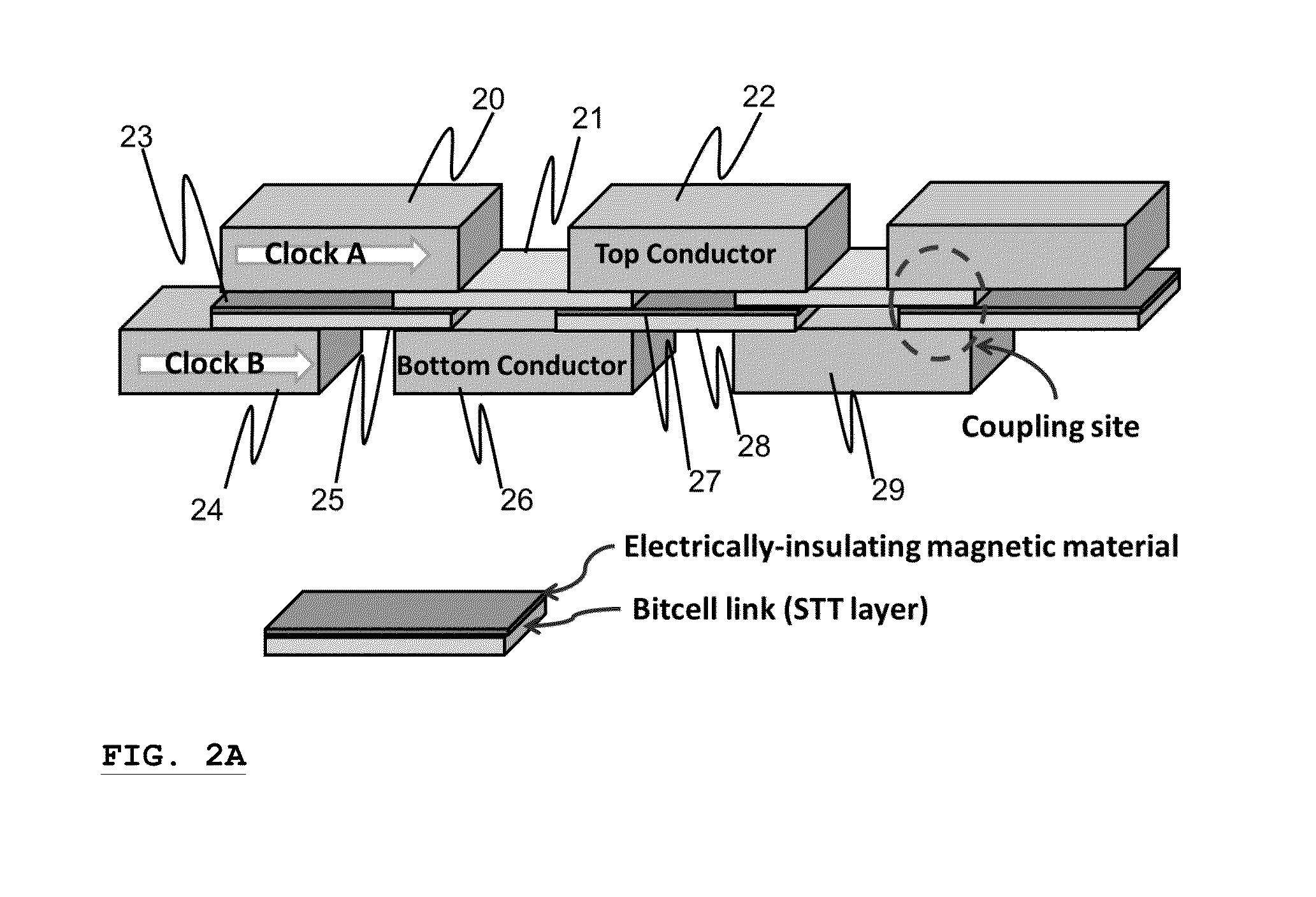
Race-track memory with improved domain wall motion control
PatentActiveKR1020220029347A
Innovation
- A race track memory layer with interleaved bit positions and domain wall traps, featuring distinct domain wall velocities and Dzyaloshinskii-Moriya Interaction (DMI) and Synthetic Antiferromagnetic (SAF) effects, along with a nonmagnetic coupling layer and ferromagnetic layer, to modulate domain wall speeds and improve control.


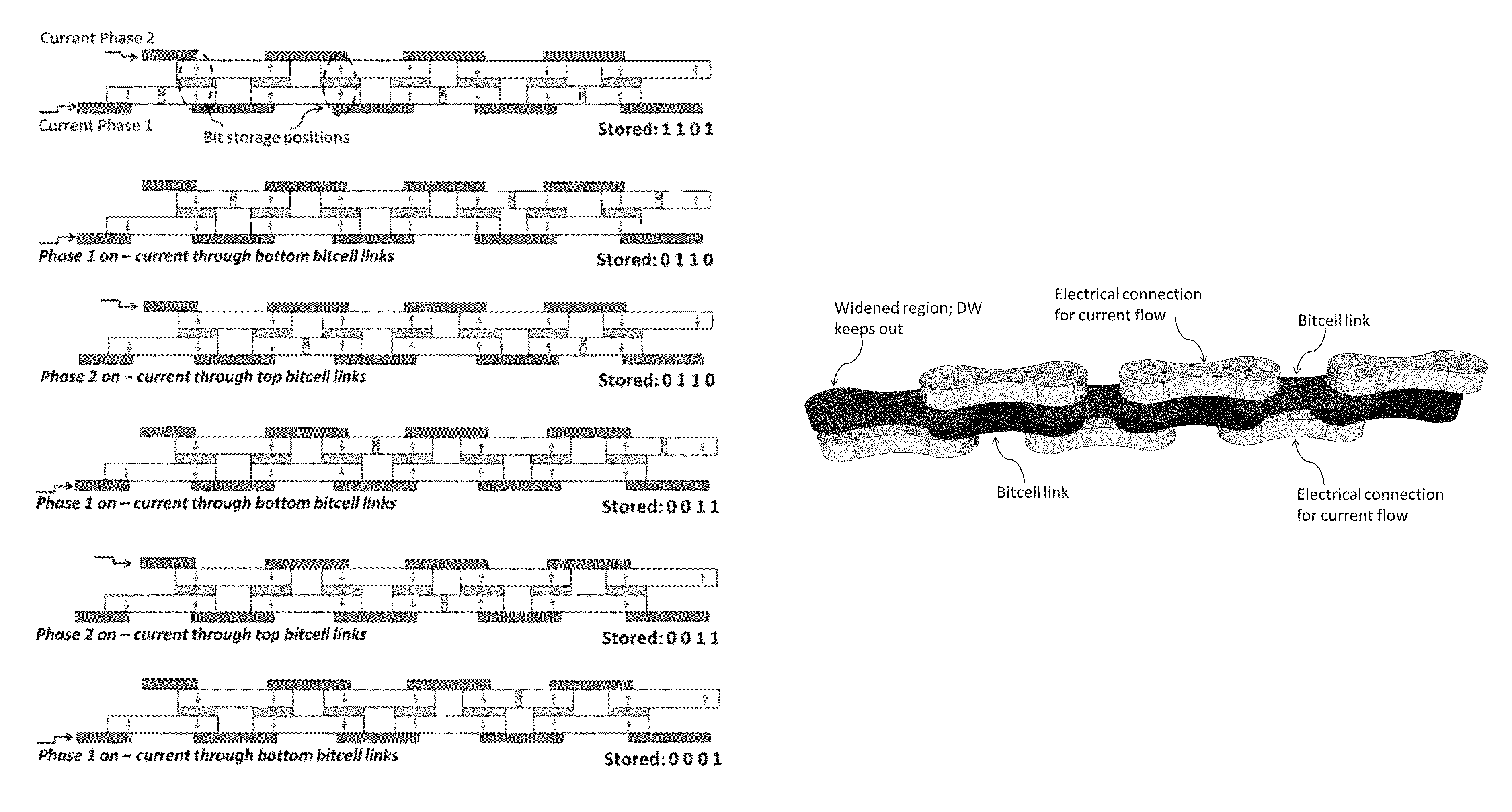
Chainlink memory
PatentInactiveUS9117523B1
Innovation
- The development of chainlink memory, where the racetrack is broken into magnetically coupled links, each handling one bit, with preferential pinning regions and unique current phases to prevent domain wall propagation and ensure data integrity, allowing for controlled bit propagation without annihilation.

Manufacturing Standards for Spintronic Memory Devices
The manufacturing of spintronic memory devices, particularly racetrack memory systems optimized with non-magnetic spacers, requires stringent standards to ensure consistent performance and reliability. Current industry standards primarily focus on material purity specifications, with non-magnetic spacer materials requiring impurity levels below 10 parts per million to prevent unwanted magnetic interactions that could compromise domain wall motion.
Dimensional tolerances represent another critical manufacturing parameter. Non-magnetic spacer thickness must be controlled within ±0.5 nanometers to maintain uniform magnetic coupling between ferromagnetic layers. This precision demands advanced deposition techniques such as atomic layer deposition or molecular beam epitaxy, which can achieve the required uniformity across wafer-scale production.
Interface quality standards mandate surface roughness below 0.2 nanometers RMS to minimize scattering effects that degrade spin transport efficiency. Manufacturing protocols typically incorporate in-situ surface cleaning procedures and controlled atmosphere processing to achieve these specifications. Temperature control during deposition must remain within ±2°C to ensure consistent crystallographic properties.
Electrical characterization standards require resistance measurements with precision better than 0.1% to validate proper spacer integration. Standard test structures include four-point probe configurations and transmission line methods to assess contact resistance and bulk material properties. These measurements must demonstrate reproducibility across multiple wafer lots.
Quality assurance protocols mandate statistical process control with capability indices exceeding 1.33 for critical parameters. This includes real-time monitoring of deposition rates, chamber pressure stability, and substrate temperature uniformity. Defect density specifications typically require fewer than 0.1 defects per square centimeter for production-worthy devices.
Packaging standards address environmental protection requirements, including moisture sensitivity levels and thermal cycling specifications. These standards ensure long-term reliability of the integrated non-magnetic spacer structures under operational conditions, maintaining the optimized racetrack memory performance throughout the device lifetime.
Energy Efficiency Considerations in Memory Design
Energy efficiency represents a critical design parameter in racetrack memory systems, particularly when implementing non-magnetic spacers for performance optimization. The power consumption characteristics of racetrack memory fundamentally differ from conventional memory technologies due to their unique domain wall manipulation mechanisms and the additional energy requirements introduced by spacer integration.
The primary energy consumption in racetrack memory stems from current-induced domain wall motion, where electrical pulses drive magnetic domains along nanowire tracks. Non-magnetic spacer implementation introduces additional energy considerations through modified current density requirements and altered resistance profiles. The spacer materials, typically consisting of copper, aluminum, or specialized alloys, create localized resistance variations that directly impact the energy needed for domain wall displacement.
Dynamic power consumption varies significantly based on spacer configuration and positioning. Optimally designed spacer arrays can reduce energy requirements by up to 30% compared to uniform racetrack structures, primarily through enhanced domain wall velocity and reduced current thresholds. However, poorly implemented spacers may increase power consumption due to additional scattering effects and current path modifications.
Static power considerations become particularly relevant in spacer-enhanced racetrack memory due to leakage current variations at spacer-magnetic material interfaces. The energy overhead associated with maintaining data integrity in segmented tracks requires careful thermal management and voltage regulation strategies. Advanced spacer designs incorporate energy-efficient materials with optimized conductivity profiles to minimize standby power consumption.
Comparative analysis reveals that spacer-optimized racetrack memory can achieve energy densities of 0.1-0.5 pJ per bit operation, positioning it competitively against emerging memory technologies. The energy efficiency gains become more pronounced in high-density applications where the cumulative effect of optimized domain wall dynamics significantly reduces overall system power requirements, making spacer integration a viable approach for next-generation low-power memory architectures.
Unlock deeper insights with Patsnap Eureka Quick Research — get a full tech report to explore trends and direct your research. Try now!
Generate Your Research Report Instantly with AI Agent
Supercharge your innovation with Patsnap Eureka AI Agent Platform!