

Comparing Racetrack Memory vs Spin-Transfer RAM: Which Is Faster?
MAY 14, 20269 MIN READ
Generate Your Research Report Instantly with AI Agent
Patsnap Eureka helps you evaluate technical feasibility & market potential.
Racetrack Memory and STT-RAM Background and Speed Objectives
Racetrack memory and Spin-Transfer Torque Random Access Memory (STT-RAM) represent two revolutionary approaches to non-volatile memory technology, both emerging from the field of spintronics. These technologies harness electron spin properties rather than charge, offering potential solutions to the growing demands for faster, more energy-efficient memory systems in computing applications.
Racetrack memory, pioneered by IBM Research, utilizes magnetic domain walls that move along nanoscale magnetic strips or "racetracks." The technology stores data as a series of magnetic domains with alternating polarizations, where information is accessed by electrically shifting these domains past read/write heads. This concept draws inspiration from traditional magnetic tape storage but operates at the nanoscale with electronic control mechanisms.
STT-RAM builds upon magnetic tunnel junction (MTJ) technology, where data storage occurs through the manipulation of magnetic orientations in ferromagnetic layers. The technology employs spin-polarized currents to switch the magnetization state of storage elements, enabling both read and write operations. STT-RAM has evolved from earlier magnetic RAM technologies, addressing critical limitations in switching speed and power consumption.
The historical development of these technologies spans over two decades of intensive research in spintronics. Racetrack memory emerged from theoretical concepts in the early 2000s, with IBM demonstrating initial prototypes around 2008. STT-RAM development began in the late 1990s, with commercial implementations appearing in specialized applications by the 2010s.
Speed optimization objectives for both technologies center on achieving sub-nanosecond access times while maintaining non-volatility and endurance. Racetrack memory aims to combine the density advantages of storage-class memory with the speed characteristics approaching DRAM performance. The primary speed challenge involves minimizing domain wall propagation delays and optimizing the current pulses required for domain manipulation.
STT-RAM speed objectives focus on reducing switching times through optimized MTJ stack engineering and current density management. The technology targets applications requiring instant-on capabilities and frequent read/write cycles without the latency penalties associated with traditional flash memory. Critical speed parameters include write pulse duration, read access time, and thermal stability margins that affect data retention reliability.
Both technologies pursue the ultimate goal of bridging the performance gap between volatile high-speed memory and non-volatile storage, potentially revolutionizing memory hierarchies in future computing systems.
Racetrack memory, pioneered by IBM Research, utilizes magnetic domain walls that move along nanoscale magnetic strips or "racetracks." The technology stores data as a series of magnetic domains with alternating polarizations, where information is accessed by electrically shifting these domains past read/write heads. This concept draws inspiration from traditional magnetic tape storage but operates at the nanoscale with electronic control mechanisms.
STT-RAM builds upon magnetic tunnel junction (MTJ) technology, where data storage occurs through the manipulation of magnetic orientations in ferromagnetic layers. The technology employs spin-polarized currents to switch the magnetization state of storage elements, enabling both read and write operations. STT-RAM has evolved from earlier magnetic RAM technologies, addressing critical limitations in switching speed and power consumption.
The historical development of these technologies spans over two decades of intensive research in spintronics. Racetrack memory emerged from theoretical concepts in the early 2000s, with IBM demonstrating initial prototypes around 2008. STT-RAM development began in the late 1990s, with commercial implementations appearing in specialized applications by the 2010s.
Speed optimization objectives for both technologies center on achieving sub-nanosecond access times while maintaining non-volatility and endurance. Racetrack memory aims to combine the density advantages of storage-class memory with the speed characteristics approaching DRAM performance. The primary speed challenge involves minimizing domain wall propagation delays and optimizing the current pulses required for domain manipulation.
STT-RAM speed objectives focus on reducing switching times through optimized MTJ stack engineering and current density management. The technology targets applications requiring instant-on capabilities and frequent read/write cycles without the latency penalties associated with traditional flash memory. Critical speed parameters include write pulse duration, read access time, and thermal stability margins that affect data retention reliability.
Both technologies pursue the ultimate goal of bridging the performance gap between volatile high-speed memory and non-volatile storage, potentially revolutionizing memory hierarchies in future computing systems.
Market Demand Analysis for Next-Generation Memory Technologies
The global memory technology market is experiencing unprecedented demand driven by the exponential growth of data-intensive applications across multiple sectors. Cloud computing infrastructure, artificial intelligence workloads, and edge computing deployments require memory solutions that can deliver both high-speed performance and energy efficiency. Traditional memory technologies are approaching their physical and performance limits, creating substantial market opportunities for next-generation alternatives like racetrack memory and spin-transfer RAM.
Enterprise data centers represent the largest addressable market segment for advanced memory technologies. These facilities demand memory solutions capable of handling massive parallel processing workloads while maintaining low latency and high throughput. The increasing adoption of in-memory computing architectures and real-time analytics platforms has intensified the need for memory technologies that can bridge the performance gap between volatile and non-volatile storage systems.
Mobile computing and Internet of Things applications constitute another significant demand driver. Battery-powered devices require memory solutions that combine high performance with minimal power consumption. Both racetrack memory and spin-transfer RAM offer potential advantages in this space through their non-volatile characteristics and reduced standby power requirements compared to conventional DRAM technologies.
The automotive industry's transition toward autonomous vehicles and advanced driver assistance systems has created new memory requirements. These applications demand memory technologies capable of operating reliably in harsh environmental conditions while providing deterministic performance for safety-critical functions. The ability to retain data without power while delivering fast access times makes next-generation memory technologies particularly attractive for automotive applications.
High-performance computing and scientific research applications represent specialized but lucrative market segments. These domains require memory systems capable of supporting complex computational workloads with minimal bottlenecks. The unique characteristics of racetrack memory and spin-transfer RAM, including their potential for three-dimensional scaling and reduced refresh overhead, align well with the performance requirements of these demanding applications.
Market adoption patterns indicate growing interest from semiconductor manufacturers and system integrators in evaluating next-generation memory technologies. The convergence of performance requirements across different application domains suggests substantial market potential for memory solutions that can deliver superior speed, density, and energy efficiency compared to existing alternatives.
Enterprise data centers represent the largest addressable market segment for advanced memory technologies. These facilities demand memory solutions capable of handling massive parallel processing workloads while maintaining low latency and high throughput. The increasing adoption of in-memory computing architectures and real-time analytics platforms has intensified the need for memory technologies that can bridge the performance gap between volatile and non-volatile storage systems.
Mobile computing and Internet of Things applications constitute another significant demand driver. Battery-powered devices require memory solutions that combine high performance with minimal power consumption. Both racetrack memory and spin-transfer RAM offer potential advantages in this space through their non-volatile characteristics and reduced standby power requirements compared to conventional DRAM technologies.
The automotive industry's transition toward autonomous vehicles and advanced driver assistance systems has created new memory requirements. These applications demand memory technologies capable of operating reliably in harsh environmental conditions while providing deterministic performance for safety-critical functions. The ability to retain data without power while delivering fast access times makes next-generation memory technologies particularly attractive for automotive applications.
High-performance computing and scientific research applications represent specialized but lucrative market segments. These domains require memory systems capable of supporting complex computational workloads with minimal bottlenecks. The unique characteristics of racetrack memory and spin-transfer RAM, including their potential for three-dimensional scaling and reduced refresh overhead, align well with the performance requirements of these demanding applications.
Market adoption patterns indicate growing interest from semiconductor manufacturers and system integrators in evaluating next-generation memory technologies. The convergence of performance requirements across different application domains suggests substantial market potential for memory solutions that can deliver superior speed, density, and energy efficiency compared to existing alternatives.
Current State and Speed Challenges in Spintronic Memory
Spintronic memory technologies have reached a critical juncture where speed performance determines their commercial viability and competitive positioning against conventional memory solutions. Current implementations of both racetrack memory and spin-transfer torque RAM (STT-RAM) demonstrate significant variations in operational speeds, with each technology facing distinct bottlenecks that limit their theoretical performance potential.
STT-RAM has achieved the most mature development status among spintronic memories, with commercial products demonstrating write speeds ranging from 10-50 nanoseconds and read speeds as fast as 2-5 nanoseconds. However, the technology encounters fundamental speed limitations due to the stochastic nature of magnetization switching, which requires precise current pulse timing and amplitude control. The switching probability follows thermal activation models, creating inherent variability in write operations that manufacturers must compensate through error correction mechanisms.
Racetrack memory presents a more complex speed profile due to its unique domain wall motion mechanism. Current experimental implementations achieve domain wall velocities of 100-400 meters per second under applied current densities of 10^11-10^12 A/m². This translates to access times that vary significantly based on the physical distance between the read/write head and target data bit, ranging from sub-nanosecond for adjacent bits to several hundred nanoseconds for distant memory positions.
The primary speed challenge in STT-RAM stems from the write current requirements, which must overcome the magnetic anisotropy energy barrier while maintaining data retention stability. Reducing write currents to improve speed often compromises thermal stability, creating a fundamental trade-off between performance and reliability. Advanced materials engineering, including perpendicular magnetic anisotropy structures and voltage-controlled magnetic anisotropy, represents current approaches to address this limitation.
Racetrack memory faces different speed constraints related to domain wall pinning effects and current-induced heating. Structural defects in the magnetic nanowire create pinning sites that impede domain wall motion, requiring higher current densities that increase power consumption and reduce operational speed. Additionally, Joule heating from high current densities can destabilize magnetic domains and introduce thermal noise that affects switching reliability.
Both technologies struggle with scalability challenges that impact speed performance as device dimensions shrink. Increased surface-to-volume ratios in nanoscale devices amplify interface effects and magnetic fluctuations, requiring more robust switching mechanisms that often sacrifice speed for reliability in practical implementations.
STT-RAM has achieved the most mature development status among spintronic memories, with commercial products demonstrating write speeds ranging from 10-50 nanoseconds and read speeds as fast as 2-5 nanoseconds. However, the technology encounters fundamental speed limitations due to the stochastic nature of magnetization switching, which requires precise current pulse timing and amplitude control. The switching probability follows thermal activation models, creating inherent variability in write operations that manufacturers must compensate through error correction mechanisms.
Racetrack memory presents a more complex speed profile due to its unique domain wall motion mechanism. Current experimental implementations achieve domain wall velocities of 100-400 meters per second under applied current densities of 10^11-10^12 A/m². This translates to access times that vary significantly based on the physical distance between the read/write head and target data bit, ranging from sub-nanosecond for adjacent bits to several hundred nanoseconds for distant memory positions.
The primary speed challenge in STT-RAM stems from the write current requirements, which must overcome the magnetic anisotropy energy barrier while maintaining data retention stability. Reducing write currents to improve speed often compromises thermal stability, creating a fundamental trade-off between performance and reliability. Advanced materials engineering, including perpendicular magnetic anisotropy structures and voltage-controlled magnetic anisotropy, represents current approaches to address this limitation.
Racetrack memory faces different speed constraints related to domain wall pinning effects and current-induced heating. Structural defects in the magnetic nanowire create pinning sites that impede domain wall motion, requiring higher current densities that increase power consumption and reduce operational speed. Additionally, Joule heating from high current densities can destabilize magnetic domains and introduce thermal noise that affects switching reliability.
Both technologies struggle with scalability challenges that impact speed performance as device dimensions shrink. Increased surface-to-volume ratios in nanoscale devices amplify interface effects and magnetic fluctuations, requiring more robust switching mechanisms that often sacrifice speed for reliability in practical implementations.
Current Speed Solutions in Spintronic Memory Systems
01 Spin-transfer torque mechanisms for memory switching
Memory devices utilize spin-transfer torque effects to switch magnetic states in memory cells. This technology enables faster switching speeds by using spin-polarized currents to manipulate the magnetization direction of magnetic layers. The spin-transfer torque mechanism allows for reduced power consumption while maintaining high-speed operation in non-volatile memory applications.- Spin-transfer torque switching mechanisms for memory devices: Memory devices utilize spin-transfer torque mechanisms to switch magnetic states in memory cells. This technology enables faster switching speeds by using spin-polarized currents to manipulate the magnetization direction of magnetic layers. The switching process is controlled by current pulses that create sufficient torque to overcome the magnetic anisotropy, resulting in improved write speeds and reduced power consumption compared to conventional magnetic memory technologies.
- Racetrack memory architecture and domain wall motion: Racetrack memory employs magnetic domain walls that move along nanowires under the influence of spin-polarized currents. The memory architecture consists of magnetic tracks where data bits are stored as magnetic domains separated by domain walls. Current pulses are used to shift these domain walls along the track, enabling sequential access to different memory locations. This design allows for high-density storage with fast access times.
- Current-induced magnetization dynamics and speed optimization: The speed of magnetic memory devices is enhanced through optimized current-induced magnetization dynamics. Various techniques are employed to reduce switching times, including pulse shaping, current density optimization, and material engineering. The magnetization switching process is accelerated by controlling the amplitude, duration, and polarity of applied current pulses, while maintaining data integrity and minimizing power consumption.
- Memory cell structure and magnetic tunnel junction design: Advanced memory cell structures incorporate magnetic tunnel junctions with optimized layer stacks to achieve high-speed operation. The design includes free and fixed magnetic layers separated by tunnel barriers, with specific material compositions and thicknesses tailored for fast switching. Interface engineering and crystalline structure optimization contribute to reduced switching delays and improved thermal stability of the memory states.
- Write and read operation speed enhancement techniques: Various techniques are implemented to enhance both write and read operation speeds in magnetic memory systems. These include optimized sensing circuits, pre-charging schemes, and parallel processing architectures. The read operations utilize magnetoresistive effects for fast state detection, while write operations employ controlled current injection methods. Advanced control circuits and timing optimization further improve overall memory performance and reduce access latencies.
02 Racetrack memory architecture and domain wall motion
Racetrack memory employs magnetic domain walls that move along nanowires to store and access data. The architecture utilizes current-induced domain wall motion to shift magnetic domains, enabling three-dimensional memory storage with high density. This approach provides fast access times and improved data retention compared to conventional memory technologies.Expand Specific Solutions03 High-speed read and write operations optimization
Advanced techniques for optimizing read and write operations focus on reducing access latency and improving data throughput. These methods include optimized current pulse timing, enhanced sensing circuits, and improved signal processing algorithms. The optimization strategies enable faster memory operations while maintaining data integrity and reliability.Expand Specific Solutions04 Memory cell structure and material engineering
Specialized memory cell structures incorporate engineered magnetic materials and multilayer configurations to enhance performance characteristics. The cell designs feature optimized magnetic tunnel junctions, improved magnetic anisotropy, and enhanced thermal stability. These structural improvements contribute to faster switching speeds and better endurance properties.Expand Specific Solutions05 Control circuits and timing optimization for speed enhancement
Sophisticated control circuits manage the timing and sequencing of memory operations to maximize speed performance. These circuits include advanced current drivers, precision timing generators, and adaptive control algorithms. The control systems enable precise manipulation of magnetic states while minimizing switching delays and power consumption.Expand Specific Solutions
Major Players in Racetrack and STT-RAM Development
The competitive landscape for racetrack memory versus spin-transfer RAM reveals an emerging technology sector in early development stages with significant growth potential. The market remains nascent, with limited commercial deployment but substantial research investment from major players. Technology maturity varies significantly between participants, with established semiconductor giants like Intel Corp., Samsung Electronics, and IBM leading development alongside specialized memory companies such as Everspin Technologies and KIOXIA Corp. Research institutions including Max Planck Gesellschaft, Carnegie Mellon University, and Chinese Academy of Sciences Institute of Physics drive fundamental innovation, while foundries like Taiwan Semiconductor Manufacturing and emerging Chinese players like Yangtze Memory Technologies provide manufacturing capabilities. The competitive dynamics suggest a race between traditional memory architectures and next-generation solutions, with both racetrack and spin-transfer technologies competing for market adoption in high-performance computing applications.
Intel Corp.
Technical Solution: Intel has developed spin-transfer torque RAM (STT-RAM) solutions focusing on embedded memory applications and cache memory systems. Their STT-RAM technology utilizes magnetic tunnel junctions (MTJs) with perpendicular magnetic anisotropy to achieve fast switching speeds and high endurance. Intel's approach emphasizes integration with CMOS processes and has demonstrated STT-RAM cells with sub-nanosecond switching times. The company has also explored hybrid memory architectures combining STT-RAM with traditional SRAM for improved performance-power efficiency in processor caches.
Strengths: Strong CMOS integration capabilities and established semiconductor manufacturing infrastructure for STT-RAM production. Weaknesses: Higher write power requirements compared to SRAM and limited commercial deployment in mainstream products.
International Business Machines Corp.
Technical Solution: IBM pioneered racetrack memory technology, developing domain wall-based storage devices that utilize magnetic nanowires to store data in magnetic domains. Their approach involves moving domain walls using spin-polarized currents to access different memory positions along the track. IBM's racetrack memory demonstrates ultra-high density storage capabilities with non-volatile characteristics and potentially faster access times compared to traditional magnetic storage. The technology leverages spin-orbit torque mechanisms for efficient domain wall motion and has shown promising results in prototype devices with multi-bit storage per track.
Strengths: Pioneer in racetrack memory with extensive patent portfolio and proven prototype demonstrations. Weaknesses: Still in research phase with manufacturing scalability challenges and power consumption optimization needs.
Core Speed Innovations in Magnetic Domain Wall Memory
Topological Racetrack Memory having Multi-bits Storage Capability Each Unit Cell for In-memory Computing in Artificial Intelligent Inference Device
PatentPendingUS20250338504A1
Innovation
- Implementing an anti-parallel pinned (AP-pinned) storage layer with topological half Heusler alloy (THHA) materials, coupled with doping or cluster co-deposition, and laminated multilayer structures to enhance reliability and thermal stability, while using coherent spin-polarized electrical current for data storage and reading.


Racetrack memory with low-power write
PatentInactiveUS8750013B1
Innovation
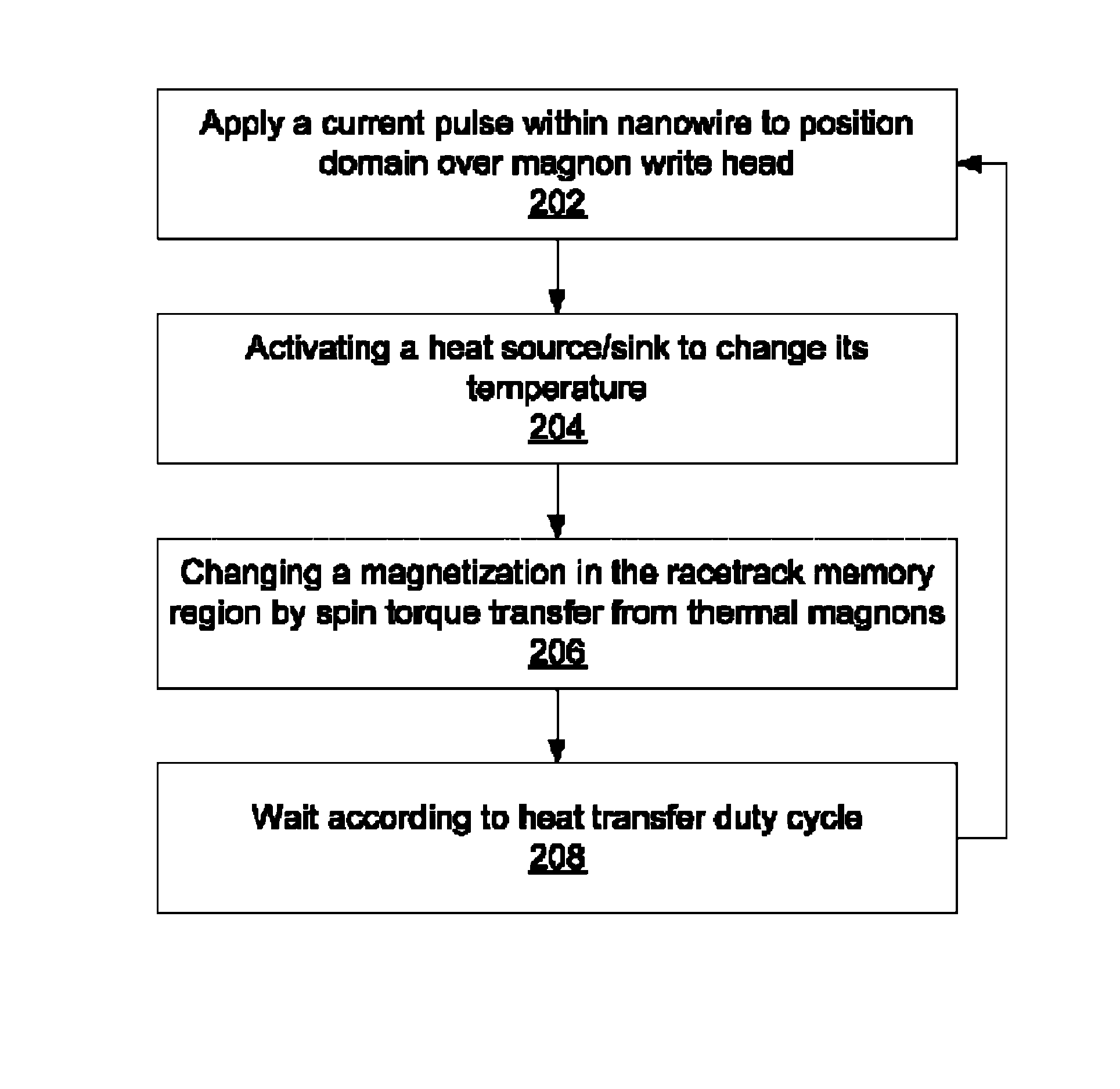
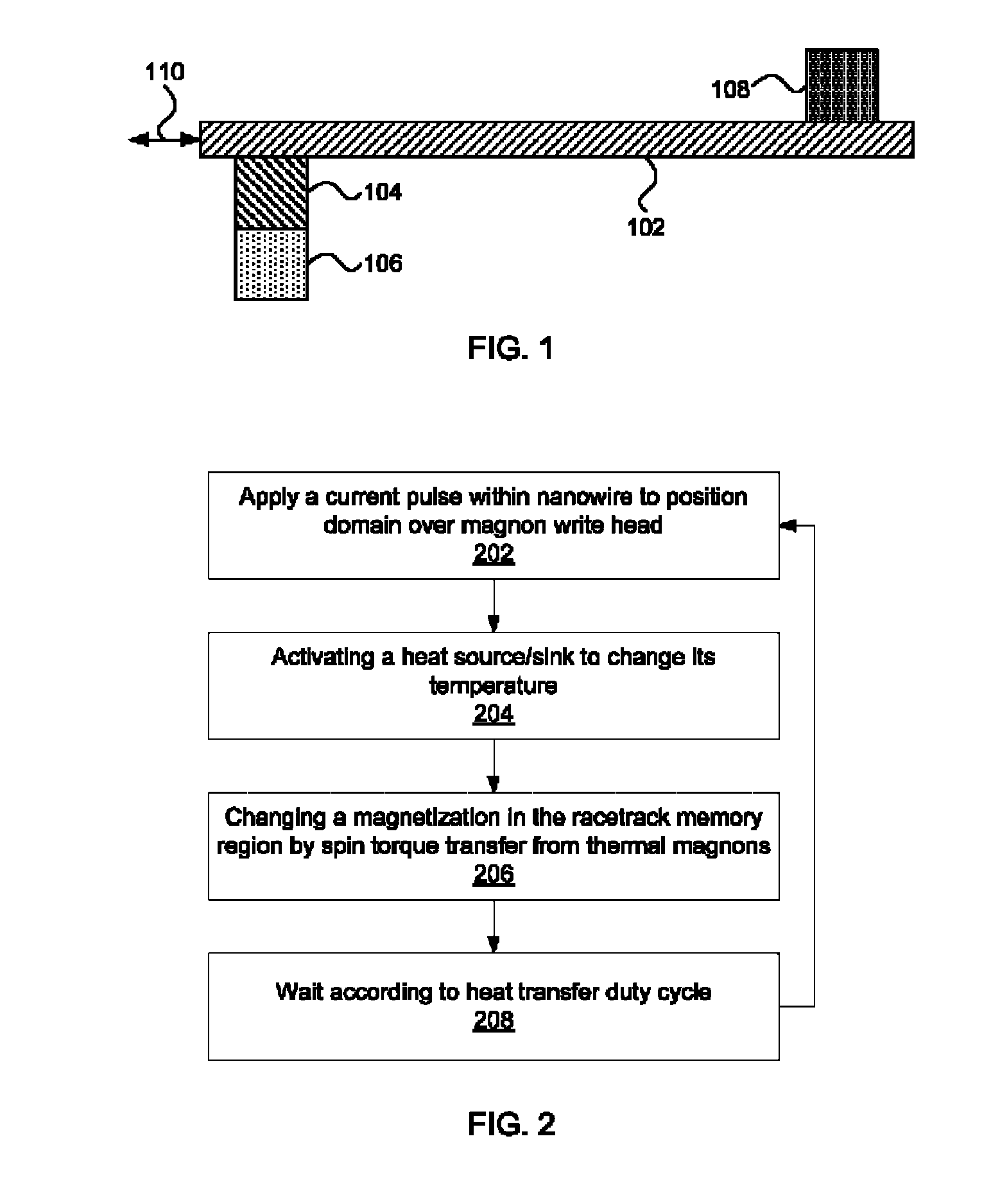
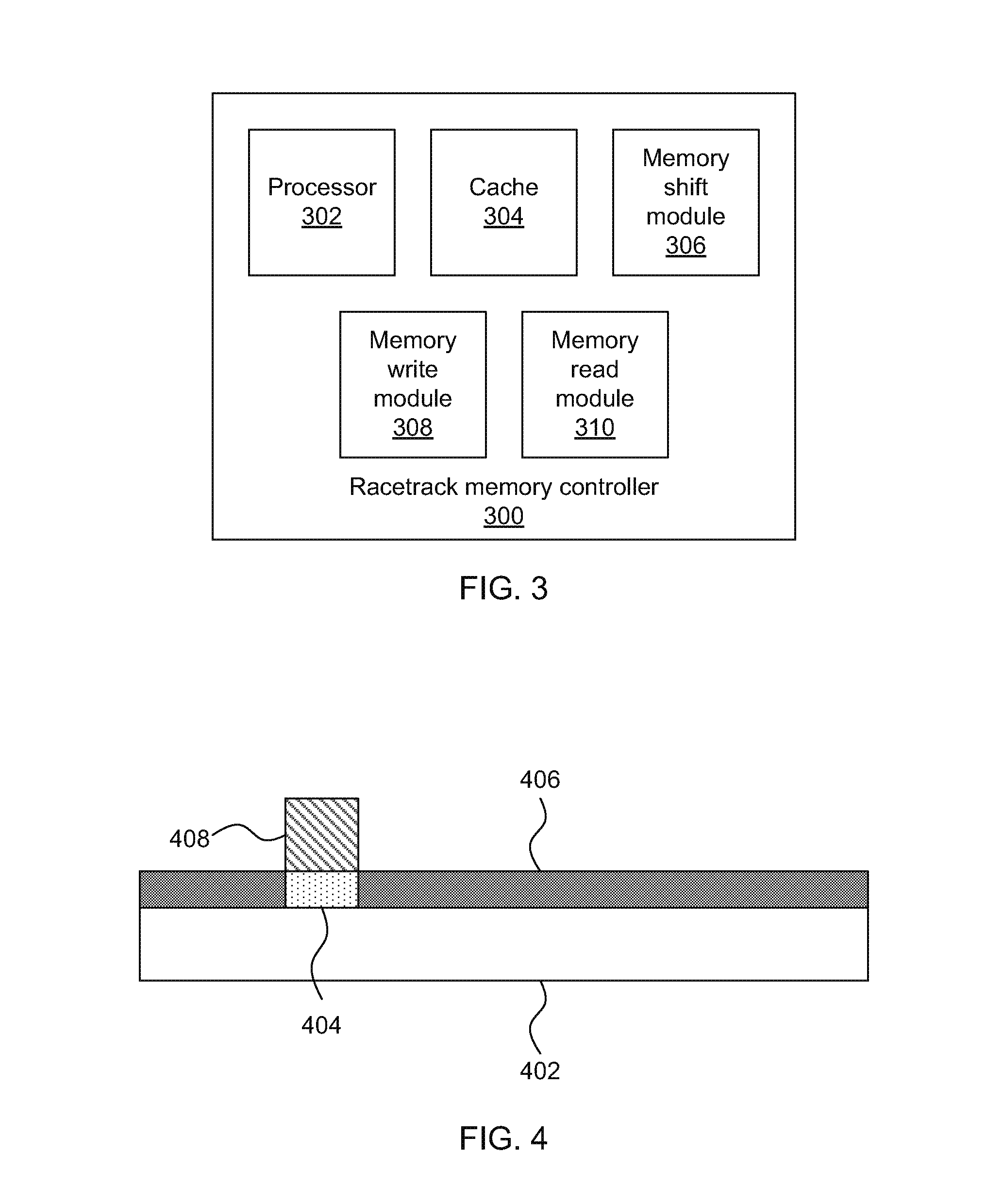
- A racetrack memory unit utilizing a heat source/sink to generate magnons, which propagate and inject domain walls through spin torque transfer, reducing the need for high currents and enhancing the stability of the memory device.

Manufacturing Process Requirements for Spintronic Memory
The manufacturing of spintronic memory devices, including both racetrack memory and spin-transfer torque RAM (STT-RAM), requires sophisticated fabrication processes that differ significantly from conventional semiconductor manufacturing. These processes must accommodate the unique material properties and structural requirements essential for spin-based information storage and manipulation.
Material deposition represents a critical manufacturing challenge for spintronic memories. The fabrication requires precise control over magnetic thin film layers, typically involving materials such as cobalt, iron, nickel alloys, and specialized compounds like CoFeB or Heusler alloys. Advanced sputtering techniques, molecular beam epitaxy, and atomic layer deposition are employed to achieve the necessary thickness uniformity and crystalline structure. Layer thickness control at the atomic scale is paramount, as variations of even a few angstroms can significantly impact device performance and reliability.
Lithography processes for spintronic devices demand exceptional precision due to the nanoscale dimensions required for optimal magnetic domain control. Electron beam lithography and extreme ultraviolet lithography are frequently utilized to define magnetic tunnel junction structures and nanowire geometries. The critical dimensions often approach 10-20 nanometers, requiring advanced resist materials and multi-step patterning techniques to achieve the necessary resolution and edge roughness control.
Etching processes present unique challenges in spintronic manufacturing, particularly regarding magnetic material compatibility. Ion beam etching and reactive ion etching must be carefully optimized to prevent magnetic property degradation while maintaining dimensional accuracy. The etching chemistry and plasma conditions require precise tuning to avoid redeposition effects and ensure clean sidewall profiles, which are crucial for maintaining magnetic isolation between adjacent devices.
Thermal processing considerations are particularly stringent for spintronic memories due to the temperature sensitivity of magnetic interfaces and tunnel barriers. Annealing processes must balance crystallization requirements with interface stability, often requiring rapid thermal processing or laser annealing techniques. Temperature gradients and processing atmospheres must be carefully controlled to preserve the delicate magnetic properties essential for device functionality.
Quality control and metrology throughout the manufacturing process require specialized characterization techniques including magnetic force microscopy, vibrating sample magnetometry, and electrical testing of magnetic tunnel junctions. These measurements ensure that the magnetic properties, resistance states, and switching characteristics meet the stringent specifications required for reliable memory operation.
Material deposition represents a critical manufacturing challenge for spintronic memories. The fabrication requires precise control over magnetic thin film layers, typically involving materials such as cobalt, iron, nickel alloys, and specialized compounds like CoFeB or Heusler alloys. Advanced sputtering techniques, molecular beam epitaxy, and atomic layer deposition are employed to achieve the necessary thickness uniformity and crystalline structure. Layer thickness control at the atomic scale is paramount, as variations of even a few angstroms can significantly impact device performance and reliability.
Lithography processes for spintronic devices demand exceptional precision due to the nanoscale dimensions required for optimal magnetic domain control. Electron beam lithography and extreme ultraviolet lithography are frequently utilized to define magnetic tunnel junction structures and nanowire geometries. The critical dimensions often approach 10-20 nanometers, requiring advanced resist materials and multi-step patterning techniques to achieve the necessary resolution and edge roughness control.
Etching processes present unique challenges in spintronic manufacturing, particularly regarding magnetic material compatibility. Ion beam etching and reactive ion etching must be carefully optimized to prevent magnetic property degradation while maintaining dimensional accuracy. The etching chemistry and plasma conditions require precise tuning to avoid redeposition effects and ensure clean sidewall profiles, which are crucial for maintaining magnetic isolation between adjacent devices.
Thermal processing considerations are particularly stringent for spintronic memories due to the temperature sensitivity of magnetic interfaces and tunnel barriers. Annealing processes must balance crystallization requirements with interface stability, often requiring rapid thermal processing or laser annealing techniques. Temperature gradients and processing atmospheres must be carefully controlled to preserve the delicate magnetic properties essential for device functionality.
Quality control and metrology throughout the manufacturing process require specialized characterization techniques including magnetic force microscopy, vibrating sample magnetometry, and electrical testing of magnetic tunnel junctions. These measurements ensure that the magnetic properties, resistance states, and switching characteristics meet the stringent specifications required for reliable memory operation.
Energy Efficiency Comparison in Magnetic Memory Technologies
Energy efficiency represents a critical performance metric in magnetic memory technologies, particularly when evaluating Racetrack Memory and Spin-Transfer Torque RAM (STT-RAM) for next-generation computing applications. Both technologies leverage magnetic properties for data storage but employ fundamentally different mechanisms that directly impact their power consumption profiles.
Racetrack Memory demonstrates exceptional energy efficiency through its unique domain wall motion mechanism. The technology requires minimal current pulses to shift magnetic domains along nanowires, with energy consumption primarily occurring during write operations. Read operations consume negligible power as they rely on magnetoresistive sensing without disturbing the stored data. The three-dimensional storage architecture further enhances energy efficiency by maximizing storage density per unit area, reducing the overall power required per bit stored.
STT-RAM exhibits competitive energy characteristics through its spin-polarized current switching mechanism. Write operations require controlled current injection to flip magnetic tunnel junction states, with energy consumption scaling proportionally to switching speed requirements. The technology benefits from near-zero standby power consumption due to its non-volatile nature, eliminating the need for continuous refresh cycles common in conventional memory technologies.
Comparative analysis reveals distinct energy profiles between these technologies. Racetrack Memory typically consumes 10-100 femtojoules per bit operation, with lower energy requirements for sequential access patterns due to its shift-register architecture. STT-RAM demonstrates energy consumption ranging from 1-10 picojoules per write operation, with read operations requiring significantly less power at approximately 0.1-1 picojoules per access.
The operational voltage requirements further differentiate these technologies. Racetrack Memory operates effectively at voltages below 0.5V, enabling integration with low-power CMOS processes. STT-RAM typically requires 0.8-1.2V for reliable switching, though recent advances in perpendicular magnetic anisotropy materials have reduced these requirements.
Thermal considerations significantly impact energy efficiency in both technologies. Racetrack Memory benefits from reduced heat generation due to lower current densities, while STT-RAM faces thermal challenges during high-frequency write operations that can affect switching reliability and increase energy overhead for thermal management systems.
Racetrack Memory demonstrates exceptional energy efficiency through its unique domain wall motion mechanism. The technology requires minimal current pulses to shift magnetic domains along nanowires, with energy consumption primarily occurring during write operations. Read operations consume negligible power as they rely on magnetoresistive sensing without disturbing the stored data. The three-dimensional storage architecture further enhances energy efficiency by maximizing storage density per unit area, reducing the overall power required per bit stored.
STT-RAM exhibits competitive energy characteristics through its spin-polarized current switching mechanism. Write operations require controlled current injection to flip magnetic tunnel junction states, with energy consumption scaling proportionally to switching speed requirements. The technology benefits from near-zero standby power consumption due to its non-volatile nature, eliminating the need for continuous refresh cycles common in conventional memory technologies.
Comparative analysis reveals distinct energy profiles between these technologies. Racetrack Memory typically consumes 10-100 femtojoules per bit operation, with lower energy requirements for sequential access patterns due to its shift-register architecture. STT-RAM demonstrates energy consumption ranging from 1-10 picojoules per write operation, with read operations requiring significantly less power at approximately 0.1-1 picojoules per access.
The operational voltage requirements further differentiate these technologies. Racetrack Memory operates effectively at voltages below 0.5V, enabling integration with low-power CMOS processes. STT-RAM typically requires 0.8-1.2V for reliable switching, though recent advances in perpendicular magnetic anisotropy materials have reduced these requirements.
Thermal considerations significantly impact energy efficiency in both technologies. Racetrack Memory benefits from reduced heat generation due to lower current densities, while STT-RAM faces thermal challenges during high-frequency write operations that can affect switching reliability and increase energy overhead for thermal management systems.
Unlock deeper insights with Patsnap Eureka Quick Research — get a full tech report to explore trends and direct your research. Try now!
Generate Your Research Report Instantly with AI Agent
Supercharge your innovation with Patsnap Eureka AI Agent Platform!