

Comparing Spin-Orbit Torque vs STT for Spintronic Memory Switching
JUN 5, 20269 MIN READ
Generate Your Research Report Instantly with AI Agent
Patsnap Eureka helps you evaluate technical feasibility & market potential.
Spintronic Memory Background and SOT vs STT Goals
Spintronic memory devices represent a revolutionary approach to data storage that exploits the intrinsic spin property of electrons alongside their charge. Unlike conventional semiconductor memories that rely solely on electron charge manipulation, spintronic memories utilize magnetic states to store information, offering the potential for non-volatile operation with significantly reduced power consumption. The fundamental principle involves controlling the magnetization direction of ferromagnetic layers through various torque mechanisms, enabling binary data representation through parallel or antiparallel magnetic configurations.
The evolution of spintronic memory technology has been driven by the quest to overcome the limitations of traditional memory architectures, particularly the volatile nature of DRAM and the slow write speeds of flash memory. Early developments focused on giant magnetoresistance and tunnel magnetoresistance effects, which provided the foundation for reading magnetic states with high fidelity. However, the critical challenge remained in developing efficient methods for switching these magnetic states with minimal energy expenditure and maximum reliability.
Two primary switching mechanisms have emerged as leading candidates for next-generation spintronic memory applications: Spin Transfer Torque and Spin-Orbit Torque. STT technology, which gained prominence in the early 2000s, utilizes spin-polarized current flowing perpendicular to the magnetic tunnel junction to exert torque on the free magnetic layer. This approach enabled the development of STT-MRAM devices that have already achieved commercial deployment in various applications.
SOT technology represents a more recent advancement that leverages the spin-orbit coupling effect in heavy metal layers adjacent to ferromagnetic materials. When current flows through these heavy metal layers, the strong spin-orbit interaction generates spin currents that can efficiently switch the magnetization of neighboring ferromagnetic layers. This lateral current injection approach offers distinct advantages in terms of endurance and switching efficiency compared to the perpendicular current flow required in STT devices.
The primary objectives of comparing these two switching mechanisms encompass multiple critical performance dimensions. Energy efficiency stands as a paramount concern, as the ultimate success of spintronic memories depends on achieving switching energies significantly lower than conventional technologies. Write speed represents another crucial metric, particularly for applications requiring high-performance computing capabilities. Additionally, device endurance, scalability potential, and manufacturing complexity must be thoroughly evaluated to determine the optimal path forward for commercial spintronic memory development.
The evolution of spintronic memory technology has been driven by the quest to overcome the limitations of traditional memory architectures, particularly the volatile nature of DRAM and the slow write speeds of flash memory. Early developments focused on giant magnetoresistance and tunnel magnetoresistance effects, which provided the foundation for reading magnetic states with high fidelity. However, the critical challenge remained in developing efficient methods for switching these magnetic states with minimal energy expenditure and maximum reliability.
Two primary switching mechanisms have emerged as leading candidates for next-generation spintronic memory applications: Spin Transfer Torque and Spin-Orbit Torque. STT technology, which gained prominence in the early 2000s, utilizes spin-polarized current flowing perpendicular to the magnetic tunnel junction to exert torque on the free magnetic layer. This approach enabled the development of STT-MRAM devices that have already achieved commercial deployment in various applications.
SOT technology represents a more recent advancement that leverages the spin-orbit coupling effect in heavy metal layers adjacent to ferromagnetic materials. When current flows through these heavy metal layers, the strong spin-orbit interaction generates spin currents that can efficiently switch the magnetization of neighboring ferromagnetic layers. This lateral current injection approach offers distinct advantages in terms of endurance and switching efficiency compared to the perpendicular current flow required in STT devices.
The primary objectives of comparing these two switching mechanisms encompass multiple critical performance dimensions. Energy efficiency stands as a paramount concern, as the ultimate success of spintronic memories depends on achieving switching energies significantly lower than conventional technologies. Write speed represents another crucial metric, particularly for applications requiring high-performance computing capabilities. Additionally, device endurance, scalability potential, and manufacturing complexity must be thoroughly evaluated to determine the optimal path forward for commercial spintronic memory development.
Market Demand for Advanced Spintronic Memory Solutions
The global memory market is experiencing unprecedented demand for next-generation storage solutions that can address the limitations of conventional technologies. Traditional memory architectures face significant challenges in meeting the requirements of emerging applications such as artificial intelligence, edge computing, and Internet of Things devices, which demand higher speed, lower power consumption, and enhanced endurance.
Spintronic memory technologies, particularly those utilizing Spin-Orbit Torque and Spin-Transfer Torque mechanisms, are positioned to capture substantial market opportunities across multiple sectors. The automotive industry represents a critical growth driver, where advanced driver assistance systems and autonomous vehicles require memory solutions capable of operating reliably under extreme conditions while maintaining rapid data access speeds.
Data center operators are increasingly seeking memory technologies that can reduce energy consumption while improving performance density. The comparison between SOT and STT switching mechanisms becomes particularly relevant as these facilities scale their operations and face mounting pressure to optimize power efficiency. Enterprise storage applications demand memory solutions with superior write endurance and faster switching speeds, characteristics that differentiate spintronic approaches from traditional flash memory.
Consumer electronics manufacturers are driving demand for memory technologies that enable thinner device profiles and longer battery life. Mobile devices, wearables, and portable computing systems require memory solutions that can deliver high performance within strict power budgets, making the efficiency advantages of advanced spintronic switching mechanisms increasingly valuable.
The industrial automation and robotics sectors present emerging opportunities for spintronic memory adoption, where real-time processing capabilities and radiation tolerance are essential requirements. These applications often operate in harsh environments where conventional memory technologies may experience reliability issues.
Market adoption patterns indicate growing interest from semiconductor manufacturers in developing production-ready spintronic memory solutions. The competitive landscape is intensifying as companies recognize the potential for spintronic technologies to address fundamental limitations in current memory hierarchies and enable new computing paradigms that require seamless integration of storage and processing capabilities.
Spintronic memory technologies, particularly those utilizing Spin-Orbit Torque and Spin-Transfer Torque mechanisms, are positioned to capture substantial market opportunities across multiple sectors. The automotive industry represents a critical growth driver, where advanced driver assistance systems and autonomous vehicles require memory solutions capable of operating reliably under extreme conditions while maintaining rapid data access speeds.
Data center operators are increasingly seeking memory technologies that can reduce energy consumption while improving performance density. The comparison between SOT and STT switching mechanisms becomes particularly relevant as these facilities scale their operations and face mounting pressure to optimize power efficiency. Enterprise storage applications demand memory solutions with superior write endurance and faster switching speeds, characteristics that differentiate spintronic approaches from traditional flash memory.
Consumer electronics manufacturers are driving demand for memory technologies that enable thinner device profiles and longer battery life. Mobile devices, wearables, and portable computing systems require memory solutions that can deliver high performance within strict power budgets, making the efficiency advantages of advanced spintronic switching mechanisms increasingly valuable.
The industrial automation and robotics sectors present emerging opportunities for spintronic memory adoption, where real-time processing capabilities and radiation tolerance are essential requirements. These applications often operate in harsh environments where conventional memory technologies may experience reliability issues.
Market adoption patterns indicate growing interest from semiconductor manufacturers in developing production-ready spintronic memory solutions. The competitive landscape is intensifying as companies recognize the potential for spintronic technologies to address fundamental limitations in current memory hierarchies and enable new computing paradigms that require seamless integration of storage and processing capabilities.
Current SOT and STT Technology Status and Challenges
Spin-Transfer Torque (STT) technology has achieved significant commercial maturity, particularly in STT-MRAM applications. Major manufacturers including Everspin, Samsung, and GlobalFoundries have successfully deployed STT-MRAM products ranging from embedded memory to standalone devices. Current STT implementations demonstrate switching currents in the range of 50-200 μA with switching times of 1-10 nanoseconds. The technology benefits from a relatively simple device structure requiring only two terminals, which facilitates integration with existing CMOS processes.
However, STT faces fundamental limitations that constrain its scalability and performance optimization. The primary challenge lies in the inherent trade-off between write current and data retention. Reducing the switching current typically requires lowering the magnetic anisotropy, which simultaneously decreases thermal stability and compromises data retention reliability. This creates a critical bottleneck for achieving both low-power operation and long-term data integrity.
Spin-Orbit Torque (SOT) technology represents a more recent development with promising advantages but faces distinct implementation challenges. SOT devices utilize heavy metal layers such as platinum, tantalum, or tungsten to generate spin currents through the spin Hall effect. This approach decouples the write and read paths, potentially enabling faster switching speeds and improved endurance. Laboratory demonstrations have shown SOT switching with currents as low as 10-50 μA and switching times below 1 nanosecond.
The primary technical challenge for SOT implementation is the requirement for an external magnetic field or additional mechanisms to achieve deterministic switching. Most SOT devices need either a small in-plane magnetic field or sophisticated device engineering approaches such as asymmetric device structures or exchange bias to break the symmetry and enable reliable switching between magnetic states.
Manufacturing complexity presents another significant hurdle for SOT adoption. The three-terminal device structure requires additional processing steps compared to STT devices, including precise control of heavy metal layer thickness and interface quality. The integration of SOT devices with standard CMOS processes demands careful optimization of thermal budgets and material compatibility, particularly for the heavy metal layers that are sensitive to high-temperature processing.
Both technologies face common challenges in scaling to advanced technology nodes. Interface quality between magnetic and non-magnetic layers becomes increasingly critical as device dimensions shrink. Process variations that affect magnetic properties, electrical resistance, and switching characteristics pose significant yield challenges for both STT and SOT devices.
Current research efforts focus on material engineering to address these limitations. For STT, investigations into perpendicular magnetic anisotropy materials and voltage-controlled magnetic anisotropy aim to reduce switching currents while maintaining thermal stability. SOT research emphasizes developing field-free switching mechanisms and exploring new spin-orbit materials with enhanced efficiency.
However, STT faces fundamental limitations that constrain its scalability and performance optimization. The primary challenge lies in the inherent trade-off between write current and data retention. Reducing the switching current typically requires lowering the magnetic anisotropy, which simultaneously decreases thermal stability and compromises data retention reliability. This creates a critical bottleneck for achieving both low-power operation and long-term data integrity.
Spin-Orbit Torque (SOT) technology represents a more recent development with promising advantages but faces distinct implementation challenges. SOT devices utilize heavy metal layers such as platinum, tantalum, or tungsten to generate spin currents through the spin Hall effect. This approach decouples the write and read paths, potentially enabling faster switching speeds and improved endurance. Laboratory demonstrations have shown SOT switching with currents as low as 10-50 μA and switching times below 1 nanosecond.
The primary technical challenge for SOT implementation is the requirement for an external magnetic field or additional mechanisms to achieve deterministic switching. Most SOT devices need either a small in-plane magnetic field or sophisticated device engineering approaches such as asymmetric device structures or exchange bias to break the symmetry and enable reliable switching between magnetic states.
Manufacturing complexity presents another significant hurdle for SOT adoption. The three-terminal device structure requires additional processing steps compared to STT devices, including precise control of heavy metal layer thickness and interface quality. The integration of SOT devices with standard CMOS processes demands careful optimization of thermal budgets and material compatibility, particularly for the heavy metal layers that are sensitive to high-temperature processing.
Both technologies face common challenges in scaling to advanced technology nodes. Interface quality between magnetic and non-magnetic layers becomes increasingly critical as device dimensions shrink. Process variations that affect magnetic properties, electrical resistance, and switching characteristics pose significant yield challenges for both STT and SOT devices.
Current research efforts focus on material engineering to address these limitations. For STT, investigations into perpendicular magnetic anisotropy materials and voltage-controlled magnetic anisotropy aim to reduce switching currents while maintaining thermal stability. SOT research emphasizes developing field-free switching mechanisms and exploring new spin-orbit materials with enhanced efficiency.
Existing SOT and STT Memory Switching Solutions
01 Spin-orbit torque switching mechanisms in magnetic memory devices
Magnetic memory devices utilize spin-orbit torque effects to achieve efficient switching of magnetic states. This mechanism involves the interaction between electron spin and orbital motion to generate torques that can manipulate magnetization direction in memory cells. The spin-orbit coupling creates effective magnetic fields that enable deterministic switching with reduced power consumption compared to conventional methods.- Spin-orbit torque switching mechanisms in magnetic memory devices: Magnetic memory devices utilize spin-orbit torque effects to achieve efficient switching of magnetic states. This mechanism involves the interaction between electron spin and orbital motion to generate torques that can manipulate magnetization direction in memory cells. The spin-orbit coupling creates effective magnetic fields that enable deterministic switching without requiring external magnetic fields, leading to improved energy efficiency and faster switching speeds in memory applications.
- Spin transfer torque memory cell structures and configurations: Memory devices employ specific structural configurations to optimize spin transfer torque effects for reliable data storage and retrieval. These structures typically include magnetic tunnel junctions with carefully engineered layer stacks that facilitate efficient spin-polarized current injection. The geometric and material properties of these structures are designed to minimize switching current while maintaining thermal stability and data retention characteristics.
- Combined spin-orbit and spin transfer torque switching methods: Advanced memory switching techniques integrate both spin-orbit torque and spin transfer torque mechanisms to achieve enhanced performance characteristics. This hybrid approach leverages the advantages of both phenomena to reduce switching energy, improve switching reliability, and enable more precise control over magnetization dynamics. The combination allows for optimized switching protocols that can adapt to different operational requirements and device geometries.
- Material engineering for enhanced torque efficiency: Specialized materials and material combinations are developed to maximize the efficiency of torque-based switching in magnetic memory devices. These materials exhibit strong spin-orbit coupling or enhanced spin polarization properties that amplify the torque effects. Material selection and engineering focus on optimizing interface properties, crystal structure, and electronic band structure to achieve the desired magnetic and electrical characteristics for memory applications.
- Control circuits and switching protocols for torque-based memory: Sophisticated control systems and switching protocols are implemented to precisely manage the application of spin-orbit torque and spin transfer torque in memory operations. These systems include current pulse generation circuits, timing control mechanisms, and feedback systems that ensure reliable and repeatable switching behavior. The control protocols are designed to minimize power consumption while maintaining fast switching speeds and high endurance for practical memory applications.
02 Spin transfer torque memory cell structures and configurations
Memory devices employ specific structural configurations to optimize spin transfer torque effects for reliable data storage and retrieval. These structures include carefully designed magnetic tunnel junctions, free and reference layers, and electrode arrangements that facilitate efficient current-induced magnetization switching. The geometric and material properties are optimized to enhance switching reliability and reduce switching currents.Expand Specific Solutions03 Combined spin-orbit and spin transfer torque switching methods
Advanced memory switching techniques combine both spin-orbit torque and spin transfer torque mechanisms to achieve enhanced performance characteristics. This hybrid approach leverages the advantages of both phenomena to improve switching speed, reduce power consumption, and increase device reliability. The combined effects enable more precise control over magnetization dynamics and switching thresholds.Expand Specific Solutions04 Material engineering for enhanced torque efficiency
Specialized materials and material combinations are developed to maximize the efficiency of torque-based switching in magnetic memory devices. These materials exhibit strong spin-orbit coupling or optimized magnetic properties that enhance the generation and transfer of spin-polarized currents. Material selection and engineering directly impact the switching characteristics and overall device performance.Expand Specific Solutions05 Control circuits and switching optimization techniques
Sophisticated control methodologies and circuit designs are implemented to optimize the switching process in torque-based memory devices. These techniques include precise current pulse generation, timing control, and feedback mechanisms that ensure reliable and efficient switching operations. The control systems are designed to minimize switching errors and optimize power efficiency across different operating conditions.Expand Specific Solutions
Key Players in Spintronic Memory and MRAM Industry
The spintronic memory switching technology comparing Spin-Orbit Torque (SOT) and Spin-Transfer Torque (STT) represents an emerging sector within the broader memory industry, currently in the early commercialization phase. The market remains relatively nascent with significant growth potential as traditional memory technologies approach physical scaling limits. Technology maturity varies considerably among key players, with established semiconductor giants like Intel, Qualcomm, and IBM leading fundamental research and development, while specialized companies such as Crocus Technology and Zhejiang Hikstor focus specifically on magnetic memory commercialization. Memory manufacturers including Micron Technology, SanDisk Technologies, and Western Digital are actively exploring spintronic solutions for next-generation storage applications. Academic institutions like National University of Singapore and New York University contribute crucial research foundations, while foundries such as Taiwan Semiconductor Manufacturing and United Microelectronics provide essential fabrication capabilities for prototype and production scaling.
Intel Corp.
Technical Solution: Intel has developed comprehensive spintronic memory solutions focusing on both STT-MRAM and SOT-MRAM technologies. Their STT-MRAM approach utilizes perpendicular magnetic tunnel junctions (pMTJs) with optimized MgO barriers to achieve high tunnel magnetoresistance ratios exceeding 200%. For SOT switching, Intel explores heavy metal/ferromagnet bilayers using materials like Ta, Pt, and W as spin Hall effect generators. Their research demonstrates that SOT switching can reduce write energy by up to 10x compared to STT while maintaining nanosecond switching speeds. Intel's process integration leverages their advanced CMOS fabrication capabilities to achieve high-density memory arrays with excellent uniformity and reliability.
Strengths: Advanced CMOS integration capabilities, strong materials engineering expertise, comprehensive IP portfolio. Weaknesses: High development costs, complex manufacturing processes requiring specialized equipment.
International Business Machines Corp.
Technical Solution: IBM has pioneered research in both STT and SOT mechanisms for next-generation memory applications. Their STT-MRAM technology features innovative magnetic tunnel junction designs with synthetic antiferromagnetic reference layers and optimized free layer compositions achieving switching currents below 50μA. IBM's SOT research focuses on topological insulators and heavy metal interfaces, demonstrating field-free switching using engineered magnetic anisotropy gradients. They have developed novel three-terminal SOT devices that separate read and write paths, enabling faster switching speeds under 1ns while reducing write energy consumption by 5-10x compared to conventional STT approaches. Their materials research includes exploration of 2D materials like graphene and transition metal dichalcogenides for enhanced spin-orbit coupling effects.
Strengths: Leading fundamental research capabilities, strong materials science expertise, innovative device architectures. Weaknesses: Limited manufacturing scale compared to dedicated memory manufacturers, focus more on research than commercialization.
Core Patents in SOT vs STT Switching Mechanisms
Spin-orbit torque and spin-transfer torque magnetoresistive random-access memory stack
PatentActiveUS12016251B2
Innovation
- The integration of a spin-transfer torque (STT) MRAM stack with a spin-orbit torque (SOT) MRAM stack in series, utilizing a heavy metal rail to flip the SOT free-layer magnetic orientation in response to horizontal signals, enabling four distinct resistance states (00, 01, 10, 11) for efficient weight storage, thereby reducing power consumption and hardware requirements.
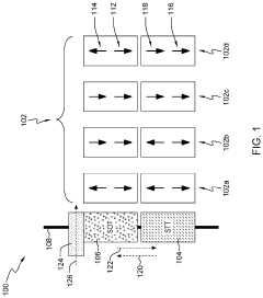
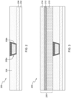
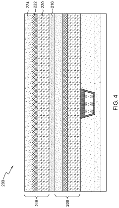
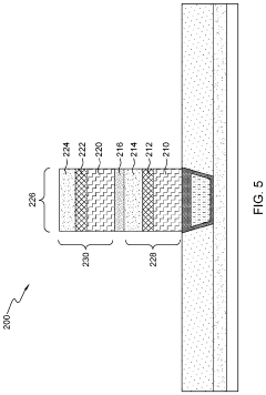
Spin transfer torque (STT) magnetic memory using spin-orbit torque (SOT)
PatentWO2019108417A1
Innovation
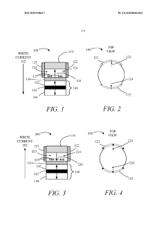
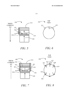
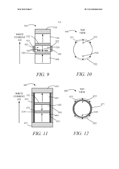
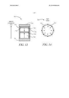
- The use of spin-orbit torque (SOT) current to assist in switching the magnetic state of the free layer in a magnetoresistive device, reducing the amount of write current needed by tilting the magnetization away from its easy axis, thereby making it more susceptible to spin-transfer torque (STT) induced switching.
Energy Efficiency Analysis of SOT vs STT Approaches
Energy efficiency represents a critical performance metric distinguishing spin-orbit torque (SOT) and spin-transfer torque (STT) approaches in spintronic memory applications. The fundamental energy consumption mechanisms differ significantly between these two switching methodologies, directly impacting their viability for next-generation memory technologies.
SOT-based switching demonstrates superior energy efficiency through its three-terminal device architecture, which decouples read and write current paths. This separation enables optimized current flow through heavy metal layers with strong spin-orbit coupling, typically requiring switching currents in the range of 10^6 to 10^7 A/cm². The write energy per bit in SOT devices typically ranges from 0.1 to 1 pJ, representing a substantial improvement over conventional approaches.
STT switching, utilizing a two-terminal configuration, requires spin-polarized current to flow directly through the magnetic tunnel junction. This approach necessitates higher current densities, often exceeding 10^7 A/cm², resulting in increased power consumption and potential reliability concerns. The write energy for STT-MRAM typically ranges from 1 to 10 pJ per switching event, significantly higher than SOT alternatives.
The switching speed characteristics further influence energy efficiency considerations. SOT devices achieve faster switching times, typically in the sub-nanosecond range, due to the enhanced spin torque efficiency and reduced critical current requirements. This rapid switching capability translates to lower dynamic energy consumption during write operations.
Thermal management considerations also favor SOT approaches, as the distributed current flow through heavy metal channels reduces localized heating effects compared to the concentrated current path in STT devices. This thermal advantage contributes to improved endurance and reduced energy losses through heat dissipation.
Scalability analysis reveals that SOT maintains its energy efficiency advantages at advanced technology nodes, while STT faces increasing challenges with dimensional scaling due to the inverse relationship between tunnel magnetoresistance and switching current requirements.
SOT-based switching demonstrates superior energy efficiency through its three-terminal device architecture, which decouples read and write current paths. This separation enables optimized current flow through heavy metal layers with strong spin-orbit coupling, typically requiring switching currents in the range of 10^6 to 10^7 A/cm². The write energy per bit in SOT devices typically ranges from 0.1 to 1 pJ, representing a substantial improvement over conventional approaches.
STT switching, utilizing a two-terminal configuration, requires spin-polarized current to flow directly through the magnetic tunnel junction. This approach necessitates higher current densities, often exceeding 10^7 A/cm², resulting in increased power consumption and potential reliability concerns. The write energy for STT-MRAM typically ranges from 1 to 10 pJ per switching event, significantly higher than SOT alternatives.
The switching speed characteristics further influence energy efficiency considerations. SOT devices achieve faster switching times, typically in the sub-nanosecond range, due to the enhanced spin torque efficiency and reduced critical current requirements. This rapid switching capability translates to lower dynamic energy consumption during write operations.
Thermal management considerations also favor SOT approaches, as the distributed current flow through heavy metal channels reduces localized heating effects compared to the concentrated current path in STT devices. This thermal advantage contributes to improved endurance and reduced energy losses through heat dissipation.
Scalability analysis reveals that SOT maintains its energy efficiency advantages at advanced technology nodes, while STT faces increasing challenges with dimensional scaling due to the inverse relationship between tunnel magnetoresistance and switching current requirements.
Scalability and Manufacturing Considerations for Spintronic Memory
The scalability of spintronic memory technologies faces distinct challenges when comparing Spin-Orbit Torque (SOT) and Spin-Transfer Torque (STT) switching mechanisms. SOT-based devices typically require three-terminal architectures with separate read and write paths, which presents unique scaling considerations. The additional heavy metal layer needed for SOT generation increases the overall device footprint and introduces complexity in vertical scaling scenarios. However, this separation of read and write operations potentially enables better endurance characteristics, which becomes increasingly important as memory arrays scale to higher densities.
STT-MRAM demonstrates superior area efficiency through its two-terminal structure, making it more compatible with conventional memory array architectures. The perpendicular magnetic tunnel junction (pMTJ) stack used in STT devices can be more readily integrated into existing CMOS processes, facilitating cost-effective manufacturing at advanced nodes. Critical dimension scaling below 20nm presents challenges for both technologies, but STT-MRAM has shown more mature development in sub-20nm demonstrations.
Manufacturing considerations reveal significant differences between the two approaches. SOT devices require precise control of heavy metal layer thickness and composition to optimize spin-orbit coupling efficiency. The interface quality between the heavy metal and ferromagnetic layers becomes critical for device performance, demanding advanced deposition techniques and thermal budget management. Process integration complexity increases due to the need for additional lithography steps and contact formation for the three-terminal structure.
STT-MRAM manufacturing benefits from established MTJ fabrication processes, with well-developed etching and annealing procedures. However, achieving uniform switching characteristics across large arrays remains challenging, particularly regarding write current distribution and thermal management. The write current requirements for STT switching can stress the access transistors, necessitating careful co-optimization of the memory cell and selection device.
Yield considerations favor different aspects of each technology. SOT devices may exhibit more uniform switching due to the decoupled read/write paths, but the increased process complexity can impact overall yield. STT-MRAM faces challenges with MTJ resistance distribution and breakdown, but benefits from simpler device structures that are more amenable to high-volume manufacturing.
STT-MRAM demonstrates superior area efficiency through its two-terminal structure, making it more compatible with conventional memory array architectures. The perpendicular magnetic tunnel junction (pMTJ) stack used in STT devices can be more readily integrated into existing CMOS processes, facilitating cost-effective manufacturing at advanced nodes. Critical dimension scaling below 20nm presents challenges for both technologies, but STT-MRAM has shown more mature development in sub-20nm demonstrations.
Manufacturing considerations reveal significant differences between the two approaches. SOT devices require precise control of heavy metal layer thickness and composition to optimize spin-orbit coupling efficiency. The interface quality between the heavy metal and ferromagnetic layers becomes critical for device performance, demanding advanced deposition techniques and thermal budget management. Process integration complexity increases due to the need for additional lithography steps and contact formation for the three-terminal structure.
STT-MRAM manufacturing benefits from established MTJ fabrication processes, with well-developed etching and annealing procedures. However, achieving uniform switching characteristics across large arrays remains challenging, particularly regarding write current distribution and thermal management. The write current requirements for STT switching can stress the access transistors, necessitating careful co-optimization of the memory cell and selection device.
Yield considerations favor different aspects of each technology. SOT devices may exhibit more uniform switching due to the decoupled read/write paths, but the increased process complexity can impact overall yield. STT-MRAM faces challenges with MTJ resistance distribution and breakdown, but benefits from simpler device structures that are more amenable to high-volume manufacturing.
Unlock deeper insights with Patsnap Eureka Quick Research — get a full tech report to explore trends and direct your research. Try now!
Generate Your Research Report Instantly with AI Agent
Supercharge your innovation with Patsnap Eureka AI Agent Platform!