

High-Density Spintronic Memory vs DRAM for Data Centers
JUN 5, 20268 MIN READ
Generate Your Research Report Instantly with AI Agent
PatSnap Eureka helps you evaluate technical feasibility & market potential.
Spintronic Memory Evolution and Data Center Goals
Spintronic memory technology has undergone significant evolution since its theoretical foundations were established in the late 20th century. The discovery of giant magnetoresistance (GMR) in 1988 and subsequent development of tunnel magnetoresistance (TMR) effects laid the groundwork for modern spintronic devices. Early magnetic random-access memory (MRAM) implementations in the 2000s demonstrated the basic principles but suffered from high switching currents and limited scalability.
The breakthrough came with spin-transfer torque MRAM (STT-MRAM) development in the 2010s, which dramatically reduced power consumption and enabled higher density integration. Recent advances in spin-orbit torque (SOT) mechanisms and perpendicular magnetic anisotropy materials have further enhanced performance characteristics, making spintronic memory a viable alternative to traditional semiconductor memory technologies.
Modern data centers face unprecedented challenges in memory hierarchy optimization. The exponential growth of data processing demands, driven by artificial intelligence, machine learning, and big data analytics, requires memory solutions that can bridge the performance gap between volatile DRAM and non-volatile storage. Current data center architectures struggle with DRAM's volatility, high refresh power consumption, and limited capacity scaling at reasonable costs.
The primary technical objectives for next-generation data center memory include achieving sub-nanosecond access times comparable to DRAM while maintaining non-volatility, scaling to multi-terabit capacities per module, and reducing overall power consumption by eliminating refresh operations. Additionally, the goal encompasses improving data retention reliability, enhancing endurance for frequent read-write cycles, and maintaining cost-effectiveness at enterprise scale.
High-density spintronic memory emerges as a promising solution to address these multifaceted requirements. The technology aims to combine DRAM-like performance with flash-like non-volatility, potentially revolutionizing data center memory architectures. Key development targets include achieving access latencies below 10 nanoseconds, scaling beyond current DRAM density limitations, and providing instant-on capabilities that eliminate lengthy boot sequences and reduce standby power consumption in cloud computing environments.
Data Center Memory Market Demand Analysis
The global data center memory market is experiencing unprecedented growth driven by the exponential expansion of cloud computing, artificial intelligence, and big data analytics. Traditional DRAM has dominated this space for decades, but emerging workloads are creating new performance and efficiency requirements that challenge conventional memory architectures. The increasing demand for real-time data processing, machine learning inference, and high-performance computing applications is pushing the boundaries of what current memory technologies can deliver.
Data centers are facing critical challenges related to memory wall limitations, where the performance gap between processors and memory continues to widen. This bottleneck significantly impacts overall system efficiency and total cost of ownership. Additionally, the growing emphasis on energy efficiency and sustainability in data center operations is driving demand for memory solutions that can deliver superior performance per watt ratios.
The market demand for high-density memory solutions is particularly acute in hyperscale data centers operated by major cloud service providers. These facilities require massive memory capacity to support virtualization, containerization, and distributed computing frameworks. Current DRAM scaling limitations and increasing costs per bit are creating opportunities for alternative memory technologies that can offer higher density and better economics.
Emerging applications such as in-memory databases, real-time analytics, and edge computing are generating new memory access patterns that favor non-volatile characteristics. The ability to maintain data persistence while delivering near-DRAM performance levels represents a significant value proposition for data center operators seeking to optimize their infrastructure investments.
The market is also responding to the need for memory solutions that can support heterogeneous computing architectures, including CPU-GPU combinations and specialized AI accelerators. These systems require memory technologies that can efficiently serve diverse workload requirements while maintaining consistent performance characteristics across different processing units.
Enterprise customers are increasingly prioritizing memory solutions that offer improved reliability, reduced maintenance overhead, and enhanced data integrity features. The growing complexity of data center workloads demands memory technologies that can provide consistent performance under varying operational conditions while supporting advanced error correction and fault tolerance mechanisms.
Current Spintronic vs DRAM Technology Status
DRAM technology has dominated data center memory architectures for decades, leveraging capacitor-based charge storage to achieve high-speed random access capabilities. Current DRAM implementations in enterprise environments typically operate at DDR4 and DDR5 standards, delivering bandwidth rates of 25.6-51.2 GB/s per module with access latencies around 10-15 nanoseconds. However, DRAM faces fundamental scaling limitations as manufacturers approach the physical boundaries of capacitor miniaturization, with current production nodes at 10-12nm experiencing increased leakage currents and reduced retention times.
The volatile nature of DRAM requires continuous power consumption for data retention, contributing significantly to data center operational costs. Modern server configurations utilizing 512GB to 2TB of DRAM per node consume approximately 20-30% of total system power solely for memory operations. Additionally, DRAM density improvements have plateaued, with current high-density modules reaching 128GB per DIMM, creating capacity bottlenecks for memory-intensive applications like in-memory databases and real-time analytics.
Spintronic memory technologies, particularly STT-MRAM and SOT-MRAM variants, represent emerging non-volatile alternatives that exploit electron spin properties for data storage. Current commercial spintronic implementations achieve densities comparable to embedded DRAM while maintaining non-volatility, with access times ranging from 20-50 nanoseconds. Leading manufacturers have demonstrated spintronic memory cells with endurance exceeding 10^15 write cycles, significantly surpassing traditional flash memory limitations.
The primary technical challenge facing spintronic memory adoption lies in write energy requirements and thermal stability. Current STT-MRAM implementations require 50-100 times more write energy than DRAM, though recent SOT-MRAM developments show promising reductions in switching currents. Manufacturing scalability remains another constraint, with most spintronic production limited to specialized foundries using modified CMOS processes.
Performance characteristics reveal distinct trade-offs between the technologies. While DRAM maintains superior bandwidth and lower access latency, spintronic memory offers instant-on capabilities, eliminating boot times and enabling persistent memory architectures. Current spintronic prototypes demonstrate read speeds approaching DRAM performance while providing the data persistence traditionally associated with storage-class memory, positioning them as potential unified memory-storage solutions for next-generation data center architectures.
Existing High-Density Memory Solutions
01 Magnetic tunnel junction structures for high-density memory
Magnetic tunnel junction structures utilize thin insulating barriers between ferromagnetic layers to create memory cells with high storage density. These structures enable precise control of magnetic states through spin-polarized tunneling effects, allowing for compact memory architectures with improved bit density per unit area.- Magnetic tunnel junction structures for high-density memory: Magnetic tunnel junction structures utilize thin insulating barriers between ferromagnetic layers to create memory cells with high storage density. These structures enable precise control of magnetic states through spin-polarized tunneling effects, allowing for compact memory architectures with improved bit density per unit area.
- Spin-transfer torque switching mechanisms: Spin-transfer torque mechanisms enable efficient switching of magnetic states in memory devices by using spin-polarized currents. This approach reduces power consumption while maintaining fast switching speeds, making it suitable for high-density memory applications where energy efficiency is critical.
- Three-dimensional memory cell architectures: Three-dimensional stacking of memory cells significantly increases storage density by utilizing vertical space in addition to horizontal layouts. These architectures incorporate multiple layers of spintronic elements to achieve higher bit densities while maintaining reliable read and write operations.
- Advanced material compositions for spintronic devices: Specialized magnetic materials and alloy compositions enhance the performance characteristics of spintronic memory devices. These materials provide improved magnetic anisotropy, thermal stability, and retention properties essential for high-density memory applications with long-term data reliability.
- Integration techniques for memory array optimization: Advanced integration methods optimize the arrangement and interconnection of spintronic memory cells within large arrays. These techniques address challenges related to cross-talk, access speed, and manufacturing scalability while maximizing the achievable memory density in practical device implementations.
02 Spin-transfer torque switching mechanisms
Spin-transfer torque mechanisms enable efficient switching of magnetic states in memory devices by using spin-polarized currents. This approach reduces power consumption while maintaining fast switching speeds, making it suitable for high-density memory applications where energy efficiency is critical.Expand Specific Solutions03 Three-dimensional memory cell architectures
Three-dimensional stacking of memory cells significantly increases storage density by utilizing vertical space in addition to planar arrangements. These architectures incorporate multiple layers of spintronic elements to achieve higher bit densities while maintaining reliable read and write operations.Expand Specific Solutions04 Advanced material compositions for spintronic devices
Specialized magnetic materials and alloy compositions enhance the performance characteristics of spintronic memory devices. These materials provide improved magnetic anisotropy, thermal stability, and retention properties essential for high-density memory applications with long-term data storage requirements.Expand Specific Solutions05 Integration methods for scalable memory arrays
Advanced fabrication and integration techniques enable the creation of large-scale spintronic memory arrays with high yield and uniformity. These methods address challenges related to device variability, cross-talk reduction, and manufacturing scalability for commercial high-density memory production.Expand Specific Solutions
Major Memory and Data Center Industry Players
The high-density spintronic memory versus DRAM competition for data centers represents an emerging technology battleground in the early commercialization stage. The market is experiencing significant growth driven by increasing data center demands, with traditional DRAM manufacturers like Samsung Electronics, SK Hynix, Micron Technology, and Intel maintaining dominant positions in the established memory market. However, technology maturity varies considerably across players. While conventional DRAM technology is highly mature with established supply chains, spintronic memory solutions remain in advanced development phases. Specialized companies like Everspin Technologies and Avalanche Technology are pioneering MRAM commercialization, while major semiconductor firms including Intel, Samsung, and research institutions like CEA and Max Planck Society are investing heavily in next-generation spintronic technologies. The competitive landscape suggests a transitional period where traditional memory giants leverage manufacturing scale while innovative startups and research organizations drive technological breakthroughs in spintronic solutions.
Intel Corp.
Technical Solution: Intel has invested heavily in 3D XPoint technology and spintronic memory research for data center applications, developing solutions that bridge the gap between DRAM and storage. Their approach to spintronic memory focuses on creating storage class memory that offers higher density than DRAM while providing significantly faster access times than traditional storage. Intel's spintronic memory strategy targets data center workloads requiring persistent memory capabilities, such as in-memory databases and real-time analytics. The company's technology emphasizes byte-addressable non-volatile memory that can reduce data center power consumption by eliminating DRAM refresh requirements while providing near-DRAM performance for specific applications.
Advantages: Strong data center market presence, proven track record in memory technologies, comprehensive platform integration. Disadvantages: 3D XPoint faced market challenges, higher latency compared to DRAM for some applications.
Samsung Electronics Co., Ltd.
Technical Solution: Samsung has developed advanced spintronic memory technologies including STT-MRAM and SOT-MRAM (Spin-Orbit Torque MRAM) for data center applications. Their approach focuses on integrating spintronic memory as a storage class memory bridge between DRAM and NAND flash, offering higher density than traditional MRAM while maintaining fast access times. Samsung's spintronic solutions target specific data center use cases such as database acceleration, persistent memory applications, and reducing DRAM refresh overhead. The company leverages its advanced semiconductor manufacturing capabilities to scale spintronic memory density while optimizing for data center power efficiency and reliability requirements.
Advantages: Advanced manufacturing capabilities, integrated memory ecosystem, strong R&D resources. Disadvantages: Still in development phase for high-density applications, faces competition from established DRAM dominance.
Core Spintronic Memory Innovations
A high density 3D magnetic memory device
PatentWO2025108583A1
Innovation
- A 3D magnetic memory device is developed, featuring a stack of dielectric and silicon-based layers with a magnetic channel that extends through the stack, allowing for the storage of multiple magnetic bits along its length. This configuration exploits all three dimensions, increasing memory density and enabling more information storage.


Multi-state spin-torque transfer magnetic random access memory
PatentInactiveUS20090218645A1
Innovation
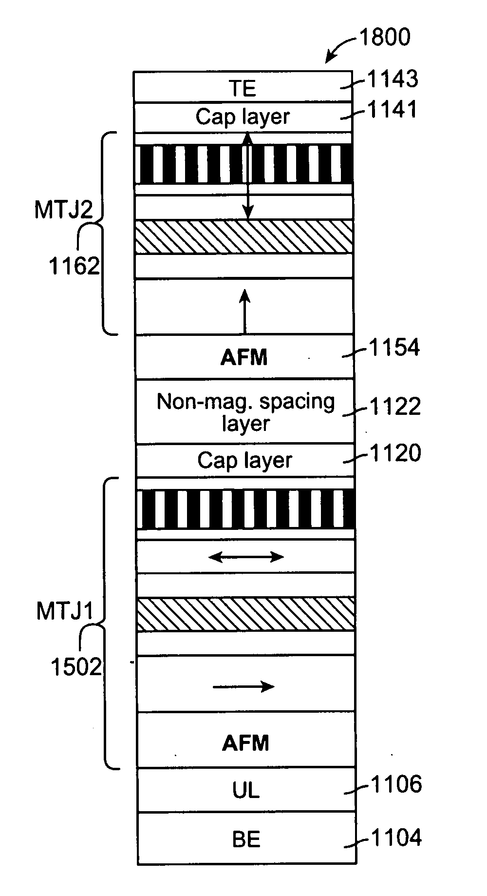
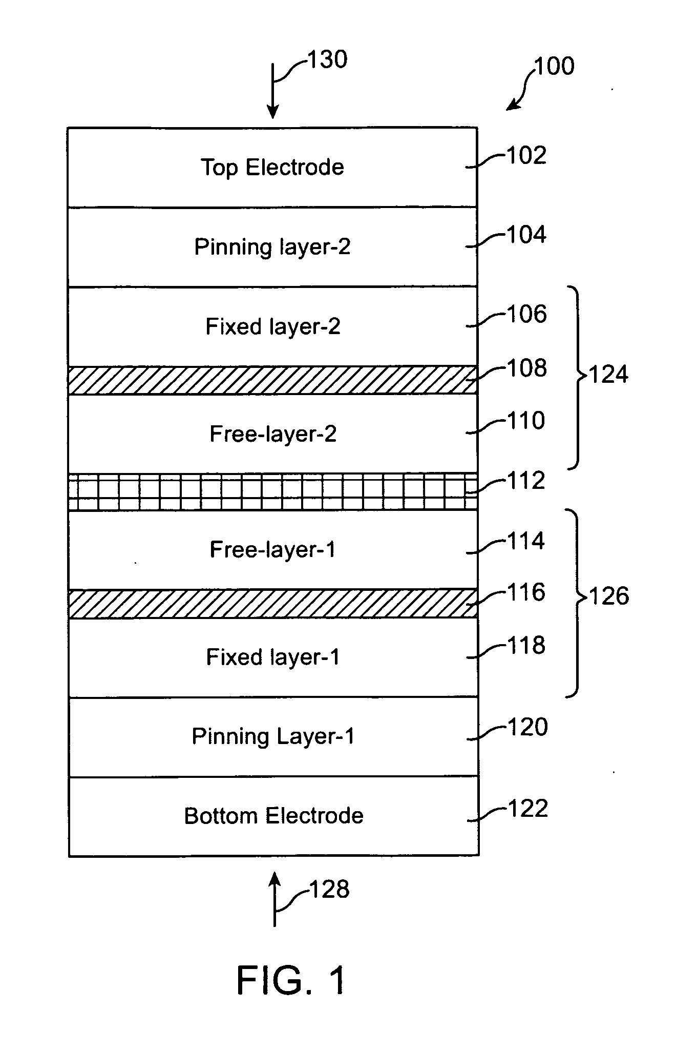
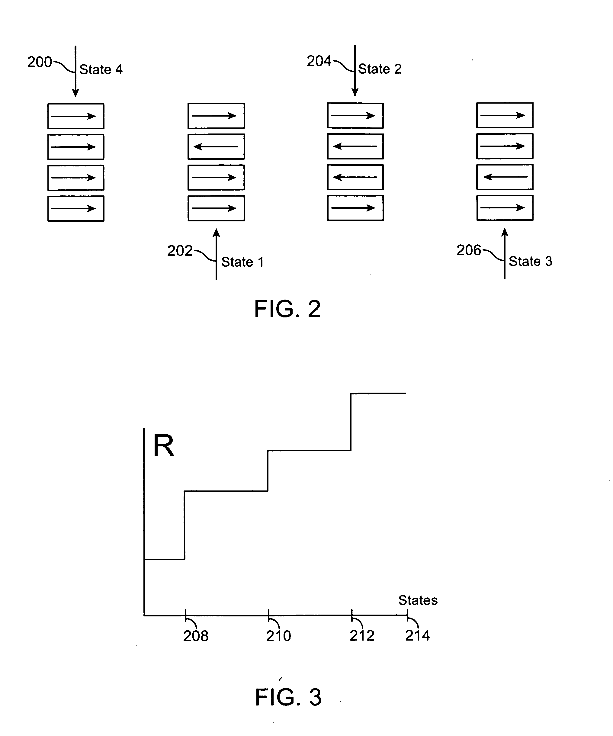
- A multi-state spin-torque transfer magnetic random access memory (STTMRAM) is developed with stacked magnetic tunnel junctions (MTJs) having magnetic anisotropy perpendicular to the plane, allowing for reduced switching current and increased thermal stability, enabling scalability down to below 30 nm.

Energy Efficiency Standards for Data Centers
The transition from DRAM to high-density spintronic memory in data centers necessitates a comprehensive reevaluation of existing energy efficiency standards. Current standards, primarily designed around volatile memory architectures, focus on metrics such as Power Usage Effectiveness (PUE) and memory power consumption per gigabyte. These frameworks inadequately address the unique energy characteristics of spintronic memory technologies, which exhibit fundamentally different power consumption patterns during read, write, and standby operations.
Spintronic memory's non-volatile nature introduces new energy efficiency paradigms that challenge conventional measurement methodologies. Unlike DRAM's continuous refresh power requirements, spintronic memory consumes energy primarily during switching operations, creating intermittent power profiles that existing standards struggle to accurately assess. This necessitates the development of dynamic energy measurement protocols that can capture the temporal variations in power consumption characteristic of spintronic devices.
International standards organizations, including IEEE and JEDEC, are actively developing new benchmarking frameworks specifically tailored to emerging memory technologies. These evolving standards emphasize total cost of ownership metrics that incorporate both operational energy consumption and embodied energy costs. The proposed frameworks introduce concepts such as "energy per bit-operation" and "standby power efficiency ratios" that better reflect spintronic memory's operational characteristics.
Regulatory compliance requirements are becoming increasingly stringent, with organizations like the European Union's Energy Efficiency Directive and the US EPA's ENERGY STAR program expanding their scope to include next-generation memory technologies. Data center operators must prepare for new certification processes that will likely mandate specific energy efficiency thresholds for spintronic memory implementations.
The establishment of these new standards will significantly influence technology adoption decisions, as compliance requirements directly impact operational licensing and potential tax incentives. Early adopters of spintronic memory technologies must navigate this evolving regulatory landscape while ensuring their implementations meet both current and anticipated future efficiency requirements.
Scalability Challenges in Memory Integration
The integration of high-density spintronic memory into existing data center architectures presents significant scalability challenges that fundamentally differ from traditional DRAM scaling approaches. Unlike DRAM's well-established manufacturing processes and standardized interfaces, spintronic memory technologies require novel integration methodologies that must accommodate their unique physical properties and operational characteristics.
Manufacturing scalability represents a primary bottleneck in spintronic memory deployment. The fabrication of magnetic tunnel junctions and spin-orbit torque devices demands precise control over nanoscale magnetic domains and interface properties. Current production yields for high-density spintronic arrays remain substantially lower than mature DRAM processes, creating cost barriers for large-scale deployment. The complexity of maintaining uniform magnetic properties across wafer-scale production introduces variability that impacts memory cell reliability and performance consistency.
Thermal management challenges intensify as spintronic memory density increases. While individual spintronic devices typically consume less power than DRAM cells, the heat dissipation patterns differ significantly due to localized current densities required for magnetic switching. High-density arrays can experience thermal gradients that affect magnetic coercivity and retention characteristics, potentially leading to data integrity issues in densely packed configurations.
Interface standardization poses another critical scalability hurdle. Existing memory controllers and bus architectures are optimized for DRAM's charge-based operation and specific timing requirements. Spintronic memory's fundamentally different read/write mechanisms and latency profiles necessitate substantial modifications to memory management units and cache hierarchies. The lack of industry-standard protocols for spintronic memory integration complicates adoption across diverse data center platforms.
Interconnect density limitations become increasingly problematic as spintronic memory arrays scale beyond current DRAM configurations. The need for specialized current drivers and sense amplifiers optimized for magnetic signal detection requires additional circuitry that can constrain achievable memory densities. Furthermore, electromagnetic interference between densely packed spintronic cells can introduce crosstalk effects that degrade signal integrity and limit practical scaling boundaries.
Error correction and reliability mechanisms must evolve to address spintronic memory's unique failure modes. Traditional ECC schemes designed for DRAM's predictable failure patterns may prove inadequate for managing magnetic domain instabilities and retention variations inherent in high-density spintronic arrays, requiring development of specialized correction algorithms and redundancy strategies.
Unlock deeper insights with PatSnap Eureka Quick Research — get a full tech report to explore trends and direct your research. Try now!
Generate Your Research Report Instantly with AI Agent
Supercharge your innovation with PatSnap Eureka AI Agent Platform!