

Spintronic Memory vs SRAM: Latency and Throughput Analysis
JUN 5, 20269 MIN READ
Generate Your Research Report Instantly with AI Agent
PatSnap Eureka helps you evaluate technical feasibility & market potential.
Spintronic Memory Development Background and Objectives
Spintronic memory technology emerged from the fundamental discovery of giant magnetoresistance (GMR) in the late 1980s, which revolutionized the understanding of electron spin manipulation in magnetic materials. This breakthrough laid the foundation for exploiting electron spin as an additional degree of freedom beyond charge, opening unprecedented possibilities for next-generation memory devices. The subsequent development of tunnel magnetoresistance (TMR) effects in magnetic tunnel junctions further accelerated the practical implementation of spintronic memory solutions.
The evolution of spintronic memory has been driven by the increasing limitations of conventional semiconductor memory technologies, particularly SRAM, in meeting the demands of modern computing systems. As device scaling approaches physical limits and power consumption becomes a critical constraint, the semiconductor industry has intensively pursued alternative memory architectures that can deliver superior performance characteristics while maintaining energy efficiency.
The primary technological objective of spintronic memory development centers on achieving non-volatile storage capabilities with performance metrics comparable to or exceeding those of volatile memory technologies like SRAM. This includes targeting sub-nanosecond switching speeds, unlimited endurance cycles, and near-zero standby power consumption. The inherent non-volatility of magnetic states provides a fundamental advantage over charge-based memory systems, eliminating the need for continuous refresh operations.
Contemporary research efforts focus on optimizing the magnetic tunnel junction structure to minimize switching latency while maximizing data retention and thermal stability. Key technical goals include reducing critical switching current densities, enhancing tunneling magnetoresistance ratios, and developing scalable fabrication processes compatible with existing CMOS technology platforms.
The strategic vision for spintronic memory encompasses creating a universal memory solution that bridges the performance gap between high-speed cache memory and non-volatile storage. This convergence aims to eliminate the traditional memory hierarchy limitations, enabling instant-on computing systems with persistent data storage capabilities. Advanced spintronic architectures, including spin-orbit torque and voltage-controlled magnetic anisotropy mechanisms, represent the next frontier in achieving these ambitious performance targets while addressing the scalability challenges of conventional spin-transfer torque approaches.
Market Demand for High-Performance Memory Solutions
The global memory market is experiencing unprecedented demand driven by the exponential growth of data-intensive applications across multiple sectors. Cloud computing infrastructure, artificial intelligence workloads, and edge computing deployments require memory solutions that can deliver exceptional performance while maintaining energy efficiency. Traditional memory hierarchies are being challenged by applications demanding both high-speed access and large-scale data processing capabilities.
Enterprise data centers represent the largest segment driving high-performance memory adoption. Modern server architectures supporting virtualization, containerization, and distributed computing frameworks require memory subsystems capable of handling massive parallel workloads. The proliferation of in-memory databases, real-time analytics platforms, and machine learning inference engines has created substantial demand for memory technologies that can bridge the performance gap between processor speeds and storage access times.
Mobile and embedded systems constitute another critical market segment where memory performance directly impacts user experience and battery life. Smartphones, tablets, and IoT devices require memory solutions that can support complex multimedia processing, augmented reality applications, and real-time sensor data processing while operating under strict power constraints. The automotive industry's transition toward autonomous vehicles and advanced driver assistance systems has further amplified demand for reliable, high-performance memory solutions capable of processing sensor fusion data in real-time.
High-performance computing applications in scientific research, financial modeling, and cryptocurrency mining continue to push memory performance boundaries. These applications often require sustained high throughput with minimal latency variations, creating opportunities for specialized memory architectures that can outperform conventional solutions in specific use cases.
The gaming industry and content creation markets demand memory solutions supporting high-resolution graphics rendering, real-time ray tracing, and 4K video processing. These applications require both high bandwidth and low latency characteristics, making them ideal testing grounds for emerging memory technologies.
Emerging technologies such as neuromorphic computing, quantum computing interfaces, and advanced robotics are creating new market niches where traditional memory solutions may prove inadequate. These applications often require memory architectures that can support novel computing paradigms while maintaining compatibility with existing software ecosystems.
Market dynamics indicate growing preference for memory solutions offering superior performance-per-watt ratios, reduced physical footprints, and enhanced reliability under extreme operating conditions. Organizations are increasingly willing to adopt innovative memory technologies that demonstrate clear performance advantages over established solutions, particularly when these benefits translate into measurable improvements in application performance and operational efficiency.
Current State of Spintronic vs SRAM Technologies
Spintronic memory technologies have emerged as promising alternatives to traditional SRAM, with several variants reaching different stages of commercial maturity. Magnetoresistive Random Access Memory (MRAM) represents the most advanced spintronic solution, with STT-MRAM (Spin-Transfer Torque MRAM) achieving commercial deployment in embedded applications since 2019. Leading manufacturers including Everspin Technologies, Samsung, and GlobalFoundries have successfully integrated STT-MRAM into production processes ranging from 28nm to 14nm nodes.
Current STT-MRAM implementations demonstrate write latencies of 10-20 nanoseconds and read latencies of 3-5 nanoseconds, positioning them between SRAM and flash memory in the memory hierarchy. However, these figures still lag behind high-performance SRAM, which achieves sub-nanosecond access times in cache applications. The endurance characteristics of STT-MRAM exceed 10^15 write cycles, significantly surpassing traditional non-volatile memories while maintaining data retention for over 10 years at operating temperatures.
SRAM technology continues to dominate high-speed cache applications despite facing significant scaling challenges below 7nm process nodes. Static power consumption has become increasingly problematic as leakage currents rise exponentially with transistor miniaturization. Advanced SRAM designs now incorporate sophisticated power management techniques, including dynamic voltage scaling and selective bit-line precharging, to mitigate these issues while maintaining performance advantages.
Emerging spintronic variants show promise for bridging the performance gap with SRAM. Voltage-Controlled Magnetic Anisotropy (VCMA) MRAM and Spin-Orbit Torque (SOT) MRAM are demonstrating improved switching speeds and reduced power consumption in laboratory settings. SOT-MRAM particularly shows potential for achieving write speeds approaching SRAM levels while maintaining non-volatility benefits.
The current technological landscape reveals complementary rather than directly competitive positioning. SRAM maintains superiority in ultra-high-speed applications requiring sub-nanosecond latencies, while spintronic memories excel in power-constrained environments where non-volatility provides system-level advantages. Manufacturing maturity favors SRAM with decades of optimization, whereas spintronic technologies are rapidly advancing through materials engineering and device architecture innovations.
Current Latency and Throughput Solutions
01 Memory cell architecture optimization for reduced latency
Spintronic memory devices utilize optimized cell architectures to minimize access latency through improved magnetic tunnel junction designs, reduced parasitic capacitance, and enhanced switching mechanisms. These architectural improvements enable faster read and write operations by reducing the time required for spin state transitions and signal propagation through the memory array.- Memory cell architecture optimization for reduced latency: Spintronic memory devices utilize optimized cell architectures to minimize access latency. These architectures focus on reducing the switching time of magnetic tunnel junctions and spin-transfer torque elements through improved electrode designs, barrier layer optimization, and enhanced magnetic anisotropy. The cell structures are designed to enable faster read and write operations while maintaining data retention and endurance characteristics.
- Write operation enhancement techniques: Advanced write mechanisms are employed to improve the throughput of spintronic memory systems. These techniques include optimized current pulse shaping, voltage-controlled magnetic anisotropy, and spin-orbit torque switching methods. The implementations focus on reducing write energy consumption while increasing write speed and reliability through precise control of magnetic domain switching processes.
- Read sensing circuit improvements: Enhanced sensing circuits and read amplifiers are developed to accelerate read operations and improve overall memory throughput. These circuits incorporate differential sensing schemes, reference cell optimization, and noise reduction techniques to enable faster and more accurate data retrieval. The designs focus on minimizing read disturb effects while maximizing sensing margin and speed.
- Memory array organization and access protocols: Optimized memory array architectures and access protocols are implemented to enhance both latency and throughput performance. These include hierarchical memory structures, parallel access schemes, and advanced addressing methods that enable concurrent operations across multiple memory banks. The designs incorporate efficient data path routing and minimize conflicts during simultaneous read and write operations.
- Interface and controller optimization: Advanced memory controllers and interface circuits are designed to maximize data transfer rates and minimize command processing delays. These systems implement sophisticated caching mechanisms, predictive algorithms, and optimized command scheduling to reduce overall system latency. The controllers manage data flow efficiently while coordinating with host systems to achieve maximum throughput performance.
02 Parallel processing and multi-level access schemes
Advanced spintronic memory systems implement parallel processing capabilities and multi-level access schemes to enhance throughput performance. These approaches allow simultaneous operations across multiple memory banks or arrays, enabling higher data transfer rates and improved overall system performance through concurrent read/write operations.Expand Specific Solutions03 Write current optimization and switching speed enhancement
Techniques for optimizing write currents and enhancing switching speeds focus on reducing the energy and time required for magnetic state transitions. These methods involve precise current pulse shaping, thermal assistance, and advanced materials engineering to achieve faster switching while maintaining data integrity and reducing power consumption.Expand Specific Solutions04 Error correction and reliability mechanisms
Spintronic memory systems incorporate sophisticated error correction codes and reliability mechanisms to maintain high throughput while ensuring data integrity. These systems implement real-time error detection and correction algorithms that operate without significantly impacting memory access speeds, enabling reliable high-performance operation.Expand Specific Solutions05 Interface and controller optimization
Memory interface and controller optimizations focus on reducing communication overhead and improving data transfer efficiency between the spintronic memory and host systems. These enhancements include advanced buffering schemes, predictive caching algorithms, and optimized command scheduling to maximize both latency and throughput performance.Expand Specific Solutions
Key Players in Spintronic and SRAM Industries
The spintronic memory versus SRAM competition represents an emerging technology landscape where traditional memory architectures face potential disruption from novel magnetic storage approaches. The industry is in early commercialization stages, with significant R&D investments from major players like Intel, Samsung Electronics, SK Hynix, and Micron Technology driving development of spintronic solutions including STT-MRAM and SOT-MRAM technologies. Market size remains nascent compared to established SRAM markets, but growing demand for non-volatile, low-power memory solutions is accelerating adoption. Technology maturity varies significantly, with companies like Qualcomm and TSMC advancing manufacturing processes while research institutions including CNRS and Max Planck Society contribute fundamental breakthroughs. Traditional memory leaders such as Samsung and SK Hynix are hedging strategies by developing both technologies, while specialized firms like Headway Technologies focus specifically on magnetic memory innovations, creating a competitive ecosystem balancing established SRAM dominance against promising spintronic alternatives.
Intel Corp.
Technical Solution: Intel has developed Spin-Transfer Torque Magnetic RAM (STT-MRAM) technology as a next-generation memory solution. Their approach focuses on integrating spintronic memory with existing CMOS processes, achieving sub-nanosecond switching speeds while maintaining non-volatility. Intel's STT-MRAM demonstrates competitive read latencies comparable to SRAM at around 1-2ns, with significantly lower standby power consumption. The company has implemented advanced magnetic tunnel junction (MTJ) designs with perpendicular magnetic anisotropy to improve thermal stability and reduce write currents. Their spintronic memory solutions target cache applications where SRAM's volatility and high leakage power present limitations, particularly in mobile and edge computing scenarios.
Strengths: Mature CMOS integration capabilities, strong process technology, established market presence. Weaknesses: Higher write latency compared to SRAM, complex manufacturing process requirements.
Samsung Electronics Co., Ltd.
Technical Solution: Samsung has pioneered commercial STT-MRAM production with their embedded MRAM (eMRAM) technology, targeting automotive and IoT applications. Their spintronic memory architecture achieves read access times of approximately 10ns while offering unlimited endurance and 10-year data retention at 150°C. Samsung's approach utilizes advanced 28nm FD-SOI process technology to integrate MRAM cells directly with logic circuits, eliminating the need for separate memory dies. The company has demonstrated throughput capabilities exceeding 1GB/s in their latest implementations, with power consumption 80% lower than equivalent SRAM solutions during standby operations. Their technology roadmap includes scaling to sub-20nm nodes while maintaining competitive performance metrics against traditional volatile memories.
Strengths: Commercial production capability, proven reliability in harsh environments, excellent data retention. Weaknesses: Higher write energy requirements, limited density compared to DRAM alternatives.
Core Patents in Spintronic Memory Performance
Spintronic devices with integrated transistors
PatentInactiveUS20110280063A1
Innovation
- A semiconductor memory device incorporating a spin-dependent logic device, such as a Giant Magneto-Resistive (GMR) device, interconnected with CMOS inverter circuits to store logic states, allowing for non-volatile operation by utilizing resistance differentials to maintain binary logic states independently of power supply.


Non-volatile static random access memory incorporating resistive random-access memory
PatentActiveUS11984158B2
Innovation
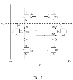
- Incorporating resistive random-access memories (RRAMs) between SRAM storage nodes and transistors, specifically between the drains of pull-up and pull-down transistors, to enable non-volatile storage without increasing the layout area, utilizing a 6T4C architecture with RRAMs positioned for setting contacts and overlapping with transistor drains.
Manufacturing Scalability Challenges
Manufacturing scalability represents one of the most significant barriers to widespread adoption of spintronic memory technologies when compared to the mature SRAM manufacturing ecosystem. Current spintronic memory fabrication requires precise control of magnetic tunnel junction (MTJ) structures at nanoscale dimensions, demanding specialized equipment and processes that differ substantially from conventional CMOS manufacturing lines.
The deposition of magnetic materials in spintronic devices presents unique challenges in achieving uniformity across large wafer areas. Unlike SRAM's well-established silicon-based processes, spintronic memory requires multiple thin-film magnetic layers with thickness variations controlled to sub-nanometer precision. This level of control becomes increasingly difficult as wafer sizes scale up to 300mm and beyond, directly impacting yield rates and manufacturing costs.
Thermal budget constraints during spintronic device fabrication create additional complexity compared to SRAM manufacturing. The magnetic properties of MTJ stacks are highly sensitive to temperature variations during subsequent processing steps, requiring careful thermal management throughout the entire fabrication sequence. This sensitivity limits the flexibility of manufacturing processes and increases the risk of device degradation during backend processing.
Integration challenges emerge when incorporating spintronic memory cells into existing CMOS foundry workflows. The magnetic materials used in spintronic devices can contaminate standard semiconductor processing equipment, necessitating dedicated fabrication lines or extensive cleaning protocols. This requirement significantly increases capital expenditure and operational complexity compared to SRAM's seamless integration with standard CMOS processes.
Yield optimization for spintronic memory faces fundamental materials science challenges that SRAM manufacturing has already overcome through decades of process refinement. Defects in magnetic layers, interface roughness, and magnetic domain variations can severely impact device performance and reliability. The statistical nature of magnetic switching processes introduces additional variability that must be controlled through advanced process monitoring and feedback systems.
Cost scaling trajectories for spintronic memory manufacturing remain unfavorable compared to SRAM's established learning curves. While SRAM benefits from shared infrastructure and process commonality with logic devices, spintronic memory requires specialized materials, equipment, and expertise that currently command premium pricing. The transition from laboratory-scale fabrication to high-volume manufacturing requires substantial investment in process development and equipment qualification, creating significant barriers for market entry and cost competitiveness.
Power Efficiency Comparison Analysis
Power consumption represents a critical differentiator between spintronic memory and SRAM technologies, with fundamental architectural differences driving distinct energy profiles. Spintronic memory devices, particularly STT-MRAM and SOT-MRAM, demonstrate superior static power efficiency due to their non-volatile nature, eliminating the continuous refresh operations required by SRAM cells. This characteristic enables spintronic memories to achieve near-zero standby power consumption, making them particularly attractive for battery-powered and edge computing applications.
SRAM exhibits significantly higher static power consumption due to its volatile storage mechanism, requiring constant power supply to maintain data integrity. The six-transistor cell structure of conventional SRAM necessitates continuous leakage current management, with power consumption scaling proportionally to memory capacity. Advanced process nodes exacerbate this challenge, as increased transistor density leads to elevated leakage currents despite voltage scaling efforts.
Dynamic power analysis reveals contrasting performance characteristics between the two technologies. SRAM demonstrates lower write energy per operation, typically ranging from 0.1 to 1 picojoule per bit, due to its charge-based switching mechanism. However, spintronic memories require higher write currents to overcome magnetic anisotropy barriers, resulting in write energies between 1 to 10 picojoules per bit, depending on the specific spintronic mechanism employed.
Read operations present a more favorable comparison for spintronic memories, with energy consumption comparable to or lower than SRAM in many implementations. The resistive sensing mechanism in spintronic devices can achieve read energies below 0.5 picojoules per bit, while maintaining non-destructive readout capabilities that eliminate refresh penalties associated with some emerging memory technologies.
Thermal efficiency considerations further distinguish these technologies, as spintronic memories typically exhibit better temperature stability and reduced cooling requirements. The magnetic storage mechanism demonstrates inherent resilience to temperature variations, potentially reducing overall system power consumption through decreased thermal management overhead compared to temperature-sensitive SRAM implementations.
Unlock deeper insights with PatSnap Eureka Quick Research — get a full tech report to explore trends and direct your research. Try now!
Generate Your Research Report Instantly with AI Agent
Supercharge your innovation with PatSnap Eureka AI Agent Platform!