

Spintronic Memory vs Flash Memory: Durability Under Extreme Loads
JUN 5, 20269 MIN READ
Generate Your Research Report Instantly with AI Agent
PatSnap Eureka helps you evaluate technical feasibility & market potential.
Spintronic vs Flash Memory Technology Background and Objectives
Memory technology has undergone significant evolution since the early days of computing, with each generation addressing specific limitations while introducing new challenges. Traditional volatile memory solutions like DRAM provided high-speed access but suffered from data loss during power interruptions. The emergence of non-volatile memory technologies marked a pivotal shift, with Flash memory becoming the dominant solution for data storage in mobile devices, solid-state drives, and embedded systems over the past two decades.
Flash memory technology, based on floating-gate transistors, revolutionized portable electronics by offering non-volatile storage with reasonable performance characteristics. However, as applications demand increasingly robust performance under extreme conditions, Flash memory's fundamental limitations have become more apparent. The technology faces significant challenges in high-radiation environments, extreme temperatures, and applications requiring millions of write-erase cycles, particularly in aerospace, automotive, and industrial control systems.
Spintronic memory represents a paradigm shift in memory technology, leveraging electron spin rather than charge for information storage. This emerging technology family, including Spin-Transfer Torque Magnetic RAM (STT-MRAM) and other spin-based variants, promises to address many limitations inherent in charge-based memory systems. The fundamental physics of spintronic devices suggests superior radiation hardness, extended temperature operating ranges, and potentially unlimited endurance cycles.
The primary objective of comparing these technologies under extreme load conditions centers on evaluating their respective durability characteristics across multiple stress factors. Extreme loads encompass high-frequency read-write operations, elevated temperatures exceeding standard operating ranges, ionizing radiation exposure, and mechanical stress conditions typical in harsh industrial environments. Understanding how each technology responds to these stressors is crucial for next-generation system design.
Current market demands increasingly require memory solutions that maintain data integrity and operational reliability in challenging environments. Space applications, autonomous vehicles, industrial IoT devices, and military systems represent growing market segments where memory durability under extreme conditions directly impacts system reliability and mission success. The evaluation framework must therefore consider not only laboratory performance metrics but also real-world application scenarios where these technologies will be deployed.
Market Demand Analysis for High-Durability Memory Solutions
The global memory market is experiencing unprecedented demand for high-durability solutions driven by the proliferation of mission-critical applications across multiple sectors. Enterprise data centers, automotive systems, aerospace applications, and industrial IoT deployments require memory technologies that can withstand extreme operational conditions while maintaining data integrity over extended periods. Traditional flash memory, despite its widespread adoption, faces significant limitations in harsh environments where temperature fluctuations, radiation exposure, and intensive read-write cycles can compromise performance and reliability.
Data center operators are increasingly seeking memory solutions that can handle continuous high-throughput operations without degradation. The exponential growth of cloud computing, artificial intelligence workloads, and real-time analytics has created substantial demand for non-volatile memory that can endure millions of program-erase cycles while maintaining consistent performance. Current flash memory technologies typically support limited write cycles, creating bottlenecks in data-intensive applications and necessitating frequent replacements that increase operational costs.
The automotive industry represents a rapidly expanding market segment for durable memory solutions. Advanced driver assistance systems, autonomous vehicle platforms, and electric vehicle control units require memory technologies capable of operating reliably across extreme temperature ranges and vibration conditions. These applications demand memory solutions that can function continuously for vehicle lifespans exceeding fifteen years while maintaining critical safety data integrity.
Aerospace and defense applications constitute another significant market driver, where memory systems must withstand radiation exposure, extreme temperatures, and mechanical stress while ensuring mission-critical data preservation. Satellite systems, avionics equipment, and military hardware require memory technologies with exceptional endurance characteristics that far exceed conventional flash memory capabilities.
Industrial automation and edge computing deployments are generating substantial demand for ruggedized memory solutions. Manufacturing environments, oil and gas operations, and smart infrastructure systems require memory technologies that can operate reliably in harsh conditions while supporting real-time data processing and storage requirements. The growing adoption of Industry 4.0 technologies is accelerating demand for memory solutions that combine high performance with exceptional durability.
Market analysis indicates strong growth potential for spintronic memory technologies that can address these durability challenges. Organizations are increasingly willing to invest in premium memory solutions that offer superior endurance characteristics, reduced maintenance requirements, and enhanced operational reliability compared to traditional flash memory alternatives.
Current Status and Challenges in Extreme Load Memory Applications
The current landscape of extreme load memory applications reveals a complex technological battleground where traditional flash memory faces mounting challenges while spintronic memory emerges as a promising alternative. Flash memory, despite its widespread adoption in consumer electronics and enterprise storage systems, demonstrates significant limitations when subjected to extreme operational conditions including high temperatures, intense radiation, and demanding write/erase cycles.
Contemporary flash memory technologies, particularly 3D NAND structures, exhibit degradation patterns under extreme loads that manifest as reduced endurance, increased error rates, and compromised data retention capabilities. The fundamental physics of charge-based storage mechanisms inherently limit flash memory's resilience, with tunnel oxide degradation and charge leakage becoming pronounced under stress conditions exceeding standard operational parameters.
Spintronic memory technologies, encompassing STT-MRAM, SOT-MRAM, and emerging variants, present fundamentally different operational principles that potentially address many limitations observed in flash memory under extreme conditions. These technologies leverage electron spin states rather than charge storage, theoretically offering superior radiation hardness, extended temperature ranges, and enhanced endurance characteristics.
Current deployment scenarios reveal that extreme load applications span aerospace systems, automotive electronics, industrial automation, and military hardware, where memory components must withstand temperature fluctuations from -55°C to 150°C, radiation exposure exceeding 100 krad, and operational lifespans extending beyond conventional consumer specifications. These demanding environments expose critical gaps in existing memory solutions.
The primary technical challenges confronting both memory technologies include thermal stability maintenance, write endurance optimization, and error correction efficiency under stress conditions. Flash memory struggles with charge retention degradation and increased bit error rates, while spintronic memory faces obstacles related to magnetic thermal fluctuations and write current optimization. Manufacturing scalability and cost considerations further complicate the adoption of spintronic alternatives in price-sensitive applications.
Geographical distribution of technological capabilities shows concentrated development in regions with advanced semiconductor manufacturing infrastructure, creating supply chain vulnerabilities for extreme load applications requiring specialized memory solutions with enhanced durability characteristics.
Current Technical Solutions for Memory Durability Enhancement
01 Spintronic memory cell structure and architecture
Advanced memory cell structures utilizing spin-based phenomena for data storage, including magnetic tunnel junctions and spin-transfer torque mechanisms. These structures enable non-volatile memory operation with improved switching characteristics and reduced power consumption compared to conventional memory technologies.- Spintronic memory cell structures and architectures: Advanced spintronic memory devices utilize specialized cell structures that leverage spin-transfer torque and magnetic tunnel junctions to achieve non-volatile data storage. These architectures incorporate magnetic layers with different coercivities and spin-polarized current paths to enable reliable switching between memory states. The cell designs focus on optimizing the magnetic anisotropy and thermal stability to enhance data retention and reduce power consumption during read and write operations.
- Flash memory endurance enhancement techniques: Various methods are employed to improve the durability and lifespan of flash memory devices by reducing wear-out mechanisms and optimizing program/erase cycles. These techniques include advanced error correction algorithms, wear leveling strategies, and voltage optimization schemes that distribute stress across memory cells more evenly. Additionally, novel programming methods and cell design modifications help minimize degradation effects such as charge trapping and oxide breakdown.
- Write endurance optimization in non-volatile memories: Specialized algorithms and control mechanisms are implemented to extend the write endurance of both spintronic and flash memory systems. These approaches involve intelligent data management, adaptive programming voltages, and dynamic threshold adjustment techniques that minimize stress on memory cells during repeated write operations. The optimization strategies also include predictive wear monitoring and proactive data migration to prevent premature failure of heavily used memory regions.
- Memory reliability and error correction mechanisms: Robust error detection and correction systems are integrated into memory architectures to maintain data integrity and extend operational lifetime. These mechanisms include advanced coding schemes, redundancy techniques, and real-time monitoring systems that can detect and compensate for various failure modes. The reliability enhancement methods also encompass temperature compensation, voltage regulation, and adaptive refresh strategies to maintain consistent performance across different operating conditions.
- Hybrid memory systems and interface optimization: Integration of different memory technologies and optimization of their interfaces to achieve improved overall system durability and performance. These hybrid approaches combine the advantages of various memory types while mitigating their individual limitations through intelligent controller designs and adaptive management algorithms. The systems incorporate dynamic allocation strategies and cross-technology wear leveling to maximize the collective endurance of the memory subsystem.
02 Flash memory endurance enhancement techniques
Methods and systems for improving the durability and lifespan of flash memory devices through advanced programming algorithms, wear leveling techniques, and error correction mechanisms. These approaches help maintain data integrity and extend the operational lifetime of memory cells under repeated program and erase cycles.Expand Specific Solutions03 Memory controller and management systems
Sophisticated control circuits and algorithms designed to optimize memory performance and reliability. These systems manage data flow, implement error detection and correction, and coordinate memory operations to ensure consistent performance and data protection across various operating conditions.Expand Specific Solutions04 Hybrid memory architectures combining different technologies
Integration of multiple memory technologies to leverage the advantages of each type while mitigating individual limitations. These hybrid approaches combine fast access times with high density storage and improved endurance characteristics for enhanced overall system performance.Expand Specific Solutions05 Memory reliability and data retention mechanisms
Techniques for ensuring long-term data stability and preventing data loss in memory devices. These mechanisms include refresh operations, redundancy schemes, and advanced materials engineering to maintain data integrity over extended periods and under various environmental conditions.Expand Specific Solutions
Major Players in Spintronic and Flash Memory Industries
The spintronic memory versus flash memory durability competition represents an emerging technology battleground in the early commercialization stage, with the global memory market exceeding $150 billion annually. While flash memory dominates current applications through established players like Samsung Electronics, Micron Technology, Intel, and KIOXIA, spintronic memory technologies including MRAM are gaining traction for extreme durability requirements. Technology maturity varies significantly - flash memory has reached industrial maturity with companies like Western Digital, Toshiba, and Taiwan Semiconductor Manufacturing providing robust solutions, while spintronic alternatives remain in advanced development phases. Key innovators like Avalanche Technology, Zhejiang Hikstor Technology, and research institutions including CEA and Electronics & Telecommunications Research Institute are driving spintronic breakthroughs. The competitive landscape suggests flash memory maintains current advantages in cost and density, but spintronic solutions show superior endurance characteristics for specialized applications requiring extreme load tolerance.
Intel Corp.
Technical Solution: Intel has invested significantly in spintronic memory research, particularly focusing on STT-MRAM and SOT-MRAM (Spin-Orbit Torque) technologies for next-generation non-volatile memory solutions. Their spintronic memory designs target extreme durability requirements with endurance levels reaching 10^12 to 10^15 write cycles, substantially outperforming NAND flash memory's typical 10^3 to 10^5 cycles. Intel's approach emphasizes integration with existing CMOS processes and optimization for data center applications where high reliability under continuous operation loads is critical. Their research demonstrates spintronic memory's ability to maintain performance stability across wide temperature ranges and under mechanical stress conditions.
Strengths: Strong semiconductor manufacturing expertise, established partnerships with major technology companies, comprehensive IP portfolio in memory technologies. Weaknesses: Limited commercial spintronic memory products currently available, competition from established flash memory market dominance.
Samsung Electronics Co., Ltd.
Technical Solution: Samsung has developed advanced spintronic memory technologies including STT-MRAM (Spin-Transfer Torque Magnetoresistive Random Access Memory) with enhanced durability characteristics. Their spintronic solutions demonstrate superior endurance compared to traditional flash memory, with write/erase cycles exceeding 10^15 operations under extreme temperature conditions ranging from -40°C to 125°C. The company's spintronic memory architecture utilizes perpendicular magnetic tunnel junctions (pMTJ) that maintain data integrity under high radiation and electromagnetic interference environments, making them suitable for aerospace and automotive applications where extreme load conditions are prevalent.
Strengths: Industry-leading manufacturing capabilities, extensive R&D investment in spintronic technologies, proven track record in memory solutions. Weaknesses: Higher production costs compared to conventional flash memory, limited commercial availability of advanced spintronic products.
Core Technology Analysis in Spintronic Memory Innovation
Magnetoelectronic devices based on colossal magnetoresistive thin films
PatentInactiveUS20070096228A1
Innovation
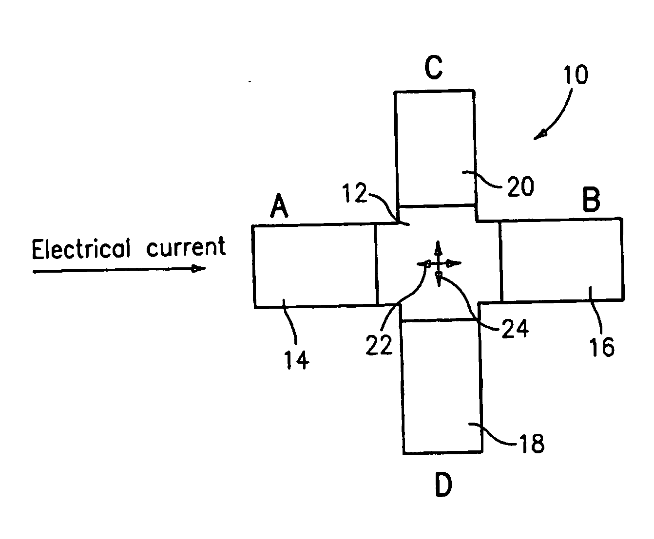
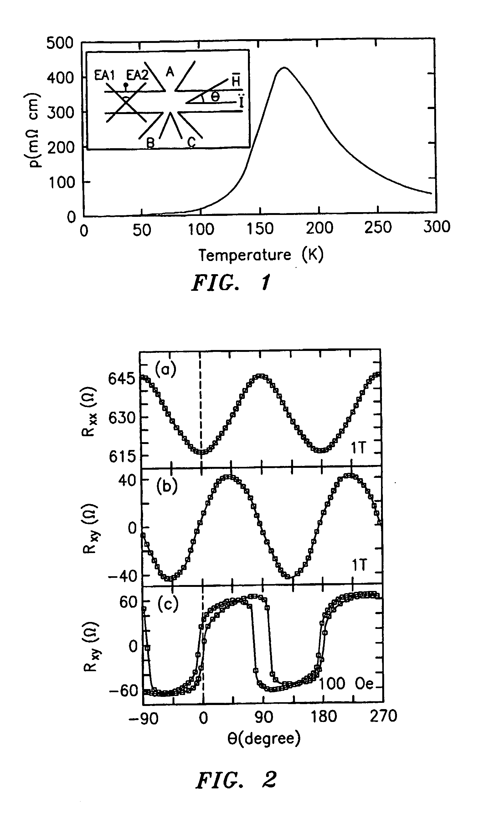
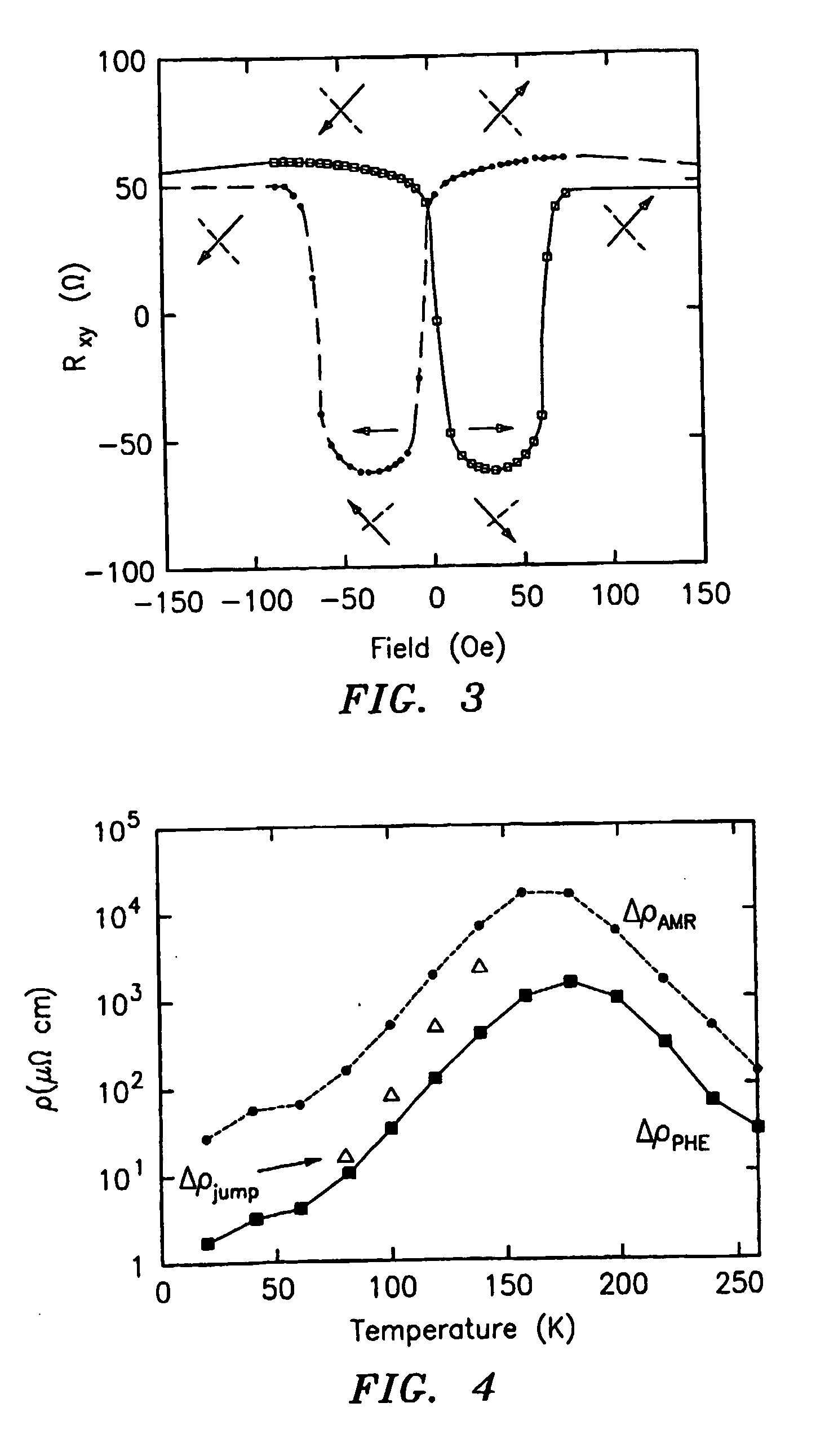
- Manganite thin films exhibiting planar Hall effect and biaxial magnetic anisotropy are used as active areas in magnetic sensors and MRAM devices, with conductive leads arranged to drive current and measure voltage, simplifying the structure and enhancing performance.

Apparatus and method for endurance of non-volatile memory banks via wear leveling in a round robin fashion
PatentActiveUS11869562B1
Innovation
- Implementing a wear leveling scheme that uses index rotation, outlier compensation, and random swap injection to distribute memory requests evenly across memory locations, combined with error correction mechanisms to enhance memory endurance and mitigate wear out attacks.


Reliability Standards and Testing Protocols for Memory Devices
Memory device reliability standards have evolved significantly to address the growing demands of modern computing applications, particularly as spintronic and flash memory technologies compete for market dominance. The Joint Electron Device Engineering Council (JEDEC) serves as the primary standardization body, establishing comprehensive testing protocols through standards such as JESD22 series for environmental stress testing and JESD47 for stress-test-driven qualification of integrated circuits.
Current reliability testing frameworks encompass multiple stress categories including thermal cycling, high-temperature operating life (HTOL), temperature humidity bias (THB), and electrostatic discharge (ESD) testing. For flash memory devices, specific protocols like JESD218A define endurance testing methodologies, while wear-leveling algorithms are evaluated under JESD219 standards. These protocols typically require devices to withstand 10,000 to 100,000 program-erase cycles depending on the application tier.
Spintronic memory devices face unique challenges in standardization due to their relatively nascent commercial deployment. Existing protocols are being adapted to address magnetic field immunity, spin-transfer torque endurance, and thermal magnetic stability. The IEEE 1149.10 standard for boundary scan testing has been extended to accommodate spintronic device characteristics, while new test methodologies are being developed to evaluate magnetic tunnel junction degradation under repetitive switching operations.
Extreme load testing protocols simulate real-world operational stresses through accelerated aging techniques. Temperature acceleration factors following Arrhenius models are commonly applied, with test temperatures ranging from 85°C to 150°C for consumer applications and up to 200°C for automotive-grade devices. Voltage stress testing employs elevated supply voltages to accelerate oxide degradation and interface trap generation, particularly critical for flash memory reliability assessment.
Data retention testing represents another crucial aspect of reliability validation, with standards requiring non-volatile memory devices to maintain data integrity for specified periods under various environmental conditions. JEDEC JESD22-A117 outlines high-temperature data retention testing, while JESD22-A108 addresses temperature cycling effects on data stability. These protocols are being refined to accommodate the different failure mechanisms observed in spintronic versus charge-based storage technologies.
Emerging reliability standards are incorporating machine learning-based predictive analytics to enhance failure detection capabilities. Advanced statistical methods including Weibull analysis and physics-of-failure modeling are being integrated into standard testing protocols to provide more accurate lifetime predictions under extreme operational scenarios.
Thermal Management Strategies in High-Performance Memory Systems
Thermal management represents a critical challenge in high-performance memory systems, particularly when comparing spintronic memory and flash memory under extreme operational loads. Both memory technologies generate substantial heat during intensive read/write operations, but their thermal characteristics and management requirements differ significantly due to their underlying physical mechanisms.
Spintronic memory devices, including STT-MRAM and SOT-MRAM, exhibit unique thermal behaviors during switching operations. The spin-transfer torque mechanism requires current densities that can reach 10^6 to 10^7 A/cm², generating localized heating effects. However, spintronic devices demonstrate superior thermal stability once programmed, with data retention capabilities extending beyond 150°C. The thermal management strategy for spintronic memory focuses on managing transient heating during write operations while leveraging the technology's inherent thermal resilience.
Flash memory systems face different thermal challenges, particularly in high-density configurations where charge trapping and tunneling mechanisms are temperature-sensitive. NAND flash performance degrades significantly above 85°C, with increased bit error rates and reduced endurance cycles. The thermal management approach for flash memory emphasizes maintaining consistent operating temperatures through active cooling and thermal spreading techniques.
Advanced thermal management strategies for high-performance memory systems incorporate multi-layered approaches. Heat spreaders and thermal interface materials optimize heat dissipation from memory dies to heat sinks. Dynamic thermal management algorithms monitor temperature sensors and adjust operational parameters, including reducing clock frequencies or implementing thermal throttling during peak load conditions.
Emerging solutions include integrated cooling technologies such as micro-channel cooling and thermoelectric coolers positioned directly adjacent to memory arrays. Phase-change materials are being explored for passive thermal regulation, absorbing excess heat during peak operations and releasing it during idle periods. Additionally, architectural innovations like 3D memory stacking require sophisticated thermal modeling to prevent hotspot formation in vertical memory structures.
The selection of thermal management strategies depends heavily on the specific memory technology, application requirements, and system constraints, with spintronic memory offering advantages in high-temperature environments while flash memory requiring more aggressive cooling solutions for sustained high-performance operations.
Unlock deeper insights with PatSnap Eureka Quick Research — get a full tech report to explore trends and direct your research. Try now!
Generate Your Research Report Instantly with AI Agent
Supercharge your innovation with PatSnap Eureka AI Agent Platform!