

Comparing Wafer Thinning Methods for Die Handling Ease
APR 7, 20269 MIN READ
Generate Your Research Report Instantly with AI Agent
Patsnap Eureka helps you evaluate technical feasibility & market potential.
Wafer Thinning Technology Background and Objectives
Wafer thinning technology has emerged as a critical process in semiconductor manufacturing, driven by the relentless pursuit of miniaturization and enhanced performance in electronic devices. The fundamental principle involves reducing the thickness of silicon wafers from their standard 725-775 micrometers to as thin as 25-100 micrometers, enabling the production of ultra-thin dies that meet the stringent requirements of modern applications.
The evolution of wafer thinning can be traced back to the early 2000s when the semiconductor industry began recognizing the need for thinner substrates to accommodate advanced packaging technologies. Initially developed for memory devices and power semiconductors, the technology has expanded across various application domains including mobile processors, sensors, and RF components. The driving forces behind this evolution include the demand for reduced package thickness, improved thermal management, and enhanced electrical performance.
Contemporary wafer thinning encompasses multiple methodologies, each presenting distinct advantages and challenges in terms of die handling characteristics. Mechanical grinding remains the most widely adopted approach, utilizing diamond wheels and precision control systems to achieve target thickness with relatively high throughput. Chemical mechanical polishing represents a hybrid solution that combines mechanical action with chemical etching to produce superior surface quality. Plasma etching technologies offer precise thickness control through reactive ion processes, while wet chemical etching provides selective material removal capabilities.
The primary objective of comparing these thinning methods centers on optimizing die handling ease throughout the manufacturing workflow. This encompasses multiple performance dimensions including die strength retention, surface roughness minimization, stress distribution uniformity, and defect density reduction. Enhanced die handling characteristics directly translate to improved yield rates during subsequent assembly processes, reduced breakage during transport and manipulation, and increased reliability in final applications.
Current technological goals focus on achieving sub-50 micrometer thickness capabilities while maintaining mechanical integrity sufficient for automated handling systems. The industry seeks to establish standardized metrics for evaluating die handling performance across different thinning approaches, enabling manufacturers to make informed process selection decisions based on specific application requirements and production constraints.
The evolution of wafer thinning can be traced back to the early 2000s when the semiconductor industry began recognizing the need for thinner substrates to accommodate advanced packaging technologies. Initially developed for memory devices and power semiconductors, the technology has expanded across various application domains including mobile processors, sensors, and RF components. The driving forces behind this evolution include the demand for reduced package thickness, improved thermal management, and enhanced electrical performance.
Contemporary wafer thinning encompasses multiple methodologies, each presenting distinct advantages and challenges in terms of die handling characteristics. Mechanical grinding remains the most widely adopted approach, utilizing diamond wheels and precision control systems to achieve target thickness with relatively high throughput. Chemical mechanical polishing represents a hybrid solution that combines mechanical action with chemical etching to produce superior surface quality. Plasma etching technologies offer precise thickness control through reactive ion processes, while wet chemical etching provides selective material removal capabilities.
The primary objective of comparing these thinning methods centers on optimizing die handling ease throughout the manufacturing workflow. This encompasses multiple performance dimensions including die strength retention, surface roughness minimization, stress distribution uniformity, and defect density reduction. Enhanced die handling characteristics directly translate to improved yield rates during subsequent assembly processes, reduced breakage during transport and manipulation, and increased reliability in final applications.
Current technological goals focus on achieving sub-50 micrometer thickness capabilities while maintaining mechanical integrity sufficient for automated handling systems. The industry seeks to establish standardized metrics for evaluating die handling performance across different thinning approaches, enabling manufacturers to make informed process selection decisions based on specific application requirements and production constraints.
Market Demand for Advanced Wafer Thinning Solutions
The semiconductor industry's relentless pursuit of miniaturization and enhanced performance has created substantial market demand for advanced wafer thinning solutions. As electronic devices become increasingly compact while requiring greater functionality, manufacturers face mounting pressure to reduce die thickness without compromising structural integrity or handling efficiency. This trend is particularly pronounced in mobile devices, wearables, and automotive electronics where space constraints drive innovation.
Market drivers for advanced wafer thinning technologies stem from multiple industry segments. The consumer electronics sector demands ultra-thin dies for smartphones, tablets, and IoT devices, where every micrometer of thickness reduction translates to valuable space savings. Memory manufacturers require precise thinning capabilities to achieve high-density 3D NAND and DRAM packaging configurations. Power semiconductor applications, especially in electric vehicles and renewable energy systems, necessitate improved thermal management through optimized die thickness control.
The packaging industry's evolution toward advanced formats such as through-silicon vias, wafer-level packaging, and system-in-package solutions has intensified requirements for uniform thinning processes. These applications demand exceptional thickness uniformity across entire wafers while maintaining die strength sufficient for subsequent handling operations. The challenge becomes more complex as wafer sizes increase and target thicknesses decrease below traditional limits.
Quality and yield considerations significantly influence market demand patterns. Manufacturers increasingly seek thinning methods that minimize subsurface damage, reduce stress-induced warpage, and maintain consistent die strength characteristics. The economic impact of improved handling ease extends beyond immediate processing benefits to encompass reduced downstream failures and enhanced assembly yields.
Emerging applications in flexible electronics, biomedical devices, and advanced sensor technologies are creating new market segments with specialized thinning requirements. These applications often demand non-traditional thickness profiles or ultra-thin configurations that challenge conventional processing approaches. The market responds by seeking innovative thinning methodologies that balance aggressive thickness reduction with practical handling constraints.
Regional market dynamics reflect varying technological priorities and manufacturing capabilities. Asian markets emphasize high-volume consumer electronics applications, while European and North American segments focus on automotive and industrial applications with stringent reliability requirements. This geographic distribution influences the specific performance characteristics most valued in advanced thinning solutions.
Market drivers for advanced wafer thinning technologies stem from multiple industry segments. The consumer electronics sector demands ultra-thin dies for smartphones, tablets, and IoT devices, where every micrometer of thickness reduction translates to valuable space savings. Memory manufacturers require precise thinning capabilities to achieve high-density 3D NAND and DRAM packaging configurations. Power semiconductor applications, especially in electric vehicles and renewable energy systems, necessitate improved thermal management through optimized die thickness control.
The packaging industry's evolution toward advanced formats such as through-silicon vias, wafer-level packaging, and system-in-package solutions has intensified requirements for uniform thinning processes. These applications demand exceptional thickness uniformity across entire wafers while maintaining die strength sufficient for subsequent handling operations. The challenge becomes more complex as wafer sizes increase and target thicknesses decrease below traditional limits.
Quality and yield considerations significantly influence market demand patterns. Manufacturers increasingly seek thinning methods that minimize subsurface damage, reduce stress-induced warpage, and maintain consistent die strength characteristics. The economic impact of improved handling ease extends beyond immediate processing benefits to encompass reduced downstream failures and enhanced assembly yields.
Emerging applications in flexible electronics, biomedical devices, and advanced sensor technologies are creating new market segments with specialized thinning requirements. These applications often demand non-traditional thickness profiles or ultra-thin configurations that challenge conventional processing approaches. The market responds by seeking innovative thinning methodologies that balance aggressive thickness reduction with practical handling constraints.
Regional market dynamics reflect varying technological priorities and manufacturing capabilities. Asian markets emphasize high-volume consumer electronics applications, while European and North American segments focus on automotive and industrial applications with stringent reliability requirements. This geographic distribution influences the specific performance characteristics most valued in advanced thinning solutions.
Current Wafer Thinning Methods and Die Handling Challenges
Wafer thinning has become an essential process in modern semiconductor manufacturing, driven by the increasing demand for miniaturized electronic devices and advanced packaging technologies. The primary objective is to reduce wafer thickness from the standard 725-775 micrometers to as thin as 25-100 micrometers, enabling the production of ultra-thin dies suitable for stacked packaging, flexible electronics, and mobile applications.
Current wafer thinning methods encompass several distinct approaches, each presenting unique advantages and challenges for subsequent die handling operations. Mechanical grinding remains the most widely adopted technique, utilizing diamond wheels to remove silicon material from the wafer backside. This method offers excellent thickness uniformity and cost-effectiveness but introduces subsurface damage and micro-cracks that can compromise die strength during handling and assembly processes.
Chemical mechanical polishing represents a refined approach that combines mechanical abrasion with chemical etching to achieve superior surface quality. While this method significantly reduces subsurface damage compared to pure grinding, it requires precise control of slurry chemistry and polishing parameters, making it more complex and time-consuming for high-volume production environments.
Plasma etching technologies, including deep reactive ion etching and atmospheric downstream plasma, provide damage-free thinning capabilities by selectively removing silicon through controlled chemical reactions. These methods preserve die mechanical integrity but face limitations in throughput and uniformity across large wafer areas, particularly for ultra-thin target thicknesses below 50 micrometers.
The primary challenge in die handling emerges from the inverse relationship between wafer thickness reduction and mechanical fragility. Thinned wafers exhibit dramatically increased susceptibility to cracking, warpage, and breakage during dicing, pick-and-place operations, and subsequent assembly steps. Surface roughness variations introduced by different thinning methods directly impact die adhesion properties and handling reliability.
Stress-induced warpage represents another critical concern, as residual stresses from thinning processes can cause wafers to bow or curl, complicating automated handling equipment operation and potentially leading to die placement errors. The selection of appropriate thinning methodology must therefore balance thickness uniformity, surface quality, throughput requirements, and downstream handling compatibility to ensure optimal manufacturing yield and product reliability.
Current wafer thinning methods encompass several distinct approaches, each presenting unique advantages and challenges for subsequent die handling operations. Mechanical grinding remains the most widely adopted technique, utilizing diamond wheels to remove silicon material from the wafer backside. This method offers excellent thickness uniformity and cost-effectiveness but introduces subsurface damage and micro-cracks that can compromise die strength during handling and assembly processes.
Chemical mechanical polishing represents a refined approach that combines mechanical abrasion with chemical etching to achieve superior surface quality. While this method significantly reduces subsurface damage compared to pure grinding, it requires precise control of slurry chemistry and polishing parameters, making it more complex and time-consuming for high-volume production environments.
Plasma etching technologies, including deep reactive ion etching and atmospheric downstream plasma, provide damage-free thinning capabilities by selectively removing silicon through controlled chemical reactions. These methods preserve die mechanical integrity but face limitations in throughput and uniformity across large wafer areas, particularly for ultra-thin target thicknesses below 50 micrometers.
The primary challenge in die handling emerges from the inverse relationship between wafer thickness reduction and mechanical fragility. Thinned wafers exhibit dramatically increased susceptibility to cracking, warpage, and breakage during dicing, pick-and-place operations, and subsequent assembly steps. Surface roughness variations introduced by different thinning methods directly impact die adhesion properties and handling reliability.
Stress-induced warpage represents another critical concern, as residual stresses from thinning processes can cause wafers to bow or curl, complicating automated handling equipment operation and potentially leading to die placement errors. The selection of appropriate thinning methodology must therefore balance thickness uniformity, surface quality, throughput requirements, and downstream handling compatibility to ensure optimal manufacturing yield and product reliability.
Existing Wafer Thinning Methods and Die Handling Solutions
01 Temporary bonding and debonding techniques for wafer thinning
Methods involving temporary bonding of wafers to carrier substrates during thinning processes, followed by controlled debonding after thinning is complete. This approach provides mechanical support during grinding and polishing operations, preventing wafer breakage and facilitating easier die handling. The temporary bonding materials can be removed through thermal, mechanical, or chemical processes without damaging the thinned wafer.- Temporary bonding and debonding methods for wafer thinning: Temporary bonding techniques involve attaching the wafer to a carrier substrate before thinning to provide mechanical support and facilitate handling of ultra-thin dies. The bonding materials can include adhesives, polymers, or wax-based compounds that can be easily removed after thinning. Debonding methods such as thermal, mechanical, or laser-assisted release enable safe separation of the thinned wafer from the carrier without damage. These techniques significantly improve die handling ease during and after the thinning process.
- Grinding and polishing techniques with protective layers: Mechanical grinding and chemical-mechanical polishing are primary wafer thinning methods that can be enhanced with protective layers applied to the wafer surface. These protective layers, such as resist coatings or protective tapes, prevent surface damage and contamination during the thinning process. The use of multi-stage grinding with progressively finer abrasives reduces subsurface damage and improves final wafer quality. Protective measures ensure that dies remain intact and are easier to handle after thinning operations.
- Dicing-before-grinding and grinding-before-dicing approaches: Dicing-before-grinding involves singulating the wafer into individual dies before the thinning process, which can reduce stress and improve yield for certain applications. Grinding-before-dicing follows the traditional approach where the wafer is thinned first and then diced. The choice between these methods affects die strength, edge quality, and handling characteristics. Advanced techniques combine both approaches with intermediate support structures to optimize die handling ease and minimize breakage during subsequent processing steps.
- Wafer mounting and support structures during thinning: Specialized mounting fixtures and support structures are designed to hold wafers securely during thinning operations while minimizing stress and deformation. These structures may include vacuum chucks, frame-based support systems, or rigid carrier plates that distribute forces evenly across the wafer. Proper mounting prevents wafer warpage and cracking, which are critical for maintaining die integrity. Enhanced support systems facilitate easier die handling by maintaining flatness and reducing the risk of damage during transfer and subsequent processing.
- Post-thinning die handling and transfer technologies: After wafer thinning, specialized handling equipment and methods are employed to safely transfer and process ultra-thin dies. These include pick-and-place systems with controlled vacuum or electrostatic gripping, automated die ejection mechanisms, and gentle release techniques that minimize mechanical stress. Surface treatments and edge reinforcement methods can be applied to improve die strength and handling robustness. Advanced transfer technologies incorporate vision systems and precision robotics to ensure accurate placement and reduce handling-related defects in thinned wafers.
02 Protective layer application before thinning
Application of protective coatings or films on the active surface of wafers prior to backside thinning operations. These protective layers shield the circuit side from contamination and mechanical damage during grinding processes. The protective materials also provide structural reinforcement that reduces wafer warpage and cracking, making subsequent die separation and handling operations more reliable.Expand Specific Solutions03 Stress relief structures and patterns
Integration of stress relief features such as grooves, trenches, or patterned structures on wafer surfaces to manage mechanical stress during and after thinning. These structures help control crack propagation and reduce wafer warpage, improving die strength and handling characteristics. The stress relief patterns can be formed before or after thinning to optimize die singulation and pickup processes.Expand Specific Solutions04 Multi-stage grinding and polishing processes
Sequential thinning approaches using multiple grinding and polishing stages with progressively finer abrasives and controlled removal rates. This gradual thinning methodology minimizes subsurface damage and residual stress in the wafer, resulting in improved die strength and reduced chipping during handling. The multi-stage process allows for better thickness uniformity and surface quality control.Expand Specific Solutions05 Dicing-before-grinding and related techniques
Processes where wafers are partially or fully diced into individual die before the backside thinning operation. This approach allows each die to be thinned while still supported by a carrier or frame structure, reducing edge chipping and improving die handling after thinning. The pre-formed separation lines facilitate easier die pickup and transfer operations in subsequent packaging steps.Expand Specific Solutions
Key Players in Wafer Thinning Equipment and Services
The wafer thinning technology landscape is in a mature growth phase, driven by increasing demand for thinner, more compact semiconductor devices in mobile and automotive applications. The market demonstrates significant scale with established players spanning equipment manufacturing, foundry services, and materials supply. Technology maturity varies across different thinning approaches, with mechanical grinding being well-established while advanced plasma-based and chemical methods continue evolving. Key equipment providers like DISCO Corp., Tokyo Seimitsu, and Applied Materials lead in precision grinding and processing technologies. Major foundries including Taiwan Semiconductor Manufacturing Co., Samsung Electronics, and Semiconductor Manufacturing International Corp. drive implementation standards. Assembly and test specialists such as Advanced Semiconductor Engineering, Siliconware Precision Industries, and STATS ChipPAC optimize post-thinning die handling processes. Materials companies like Dow Silicones Corp. and Tokyo Ohka Kogyo provide essential chemicals and protective coatings. The competitive landscape shows strong regional clusters in Asia-Pacific, with emerging players like Nexchip Semiconductor and established leaders maintaining technological differentiation through integrated process solutions and specialized equipment capabilities.
Samsung Electronics Co., Ltd.
Technical Solution: Samsung Electronics has developed comprehensive wafer thinning technologies for their advanced memory and logic devices, particularly focusing on 3D NAND and high-bandwidth memory (HBM) applications. Their thinning process combines mechanical back-grinding with plasma etching and chemical mechanical polishing to achieve ultra-thin wafers while maintaining structural integrity. Samsung's approach incorporates proprietary stress management techniques including controlled cooling systems and specialized chuck designs that prevent wafer warpage during processing. The company has implemented advanced metrology systems that provide real-time thickness monitoring and feedback control, ensuring consistent die quality and improved handling characteristics. Their integrated manufacturing approach allows for seamless transition from thinning to subsequent packaging processes, reducing handling steps and potential damage.
Strengths: Integrated manufacturing capabilities, advanced stress management, proven high-volume production. Weaknesses: Focus primarily on internal applications, limited equipment availability for external customers.
DISCO Corp.
Technical Solution: DISCO Corporation specializes in precision cutting, grinding, and polishing equipment for semiconductor wafer processing. Their wafer thinning solutions include back-grinding systems that utilize diamond wheels for mechanical thinning, achieving thickness uniformity within ±1μm across 300mm wafers. The company's DFG series grinders incorporate advanced spindle technology and automated handling systems to minimize die stress and prevent cracking during the thinning process. Their integrated approach combines grinding with subsequent processes like tape mounting and dicing, optimizing die handling ease through reduced mechanical stress and improved surface quality control.
Strengths: Industry-leading precision and thickness uniformity, integrated processing solutions. Weaknesses: Higher equipment costs, mechanical stress limitations on ultra-thin applications.
Core Technologies in Wafer Thinning Process Optimization
DBG system and method with adhesive layer severing
PatentInactiveUS20060189101A1
Innovation
- An adhesive layer is applied between the dicing tape and the grooved wafer, and a second grinding or severing step is used to sever this layer through the grooves, preventing die tilt by ensuring stable separation of individual die.


Die thinning methods
PatentInactiveUS6861336B1
Innovation
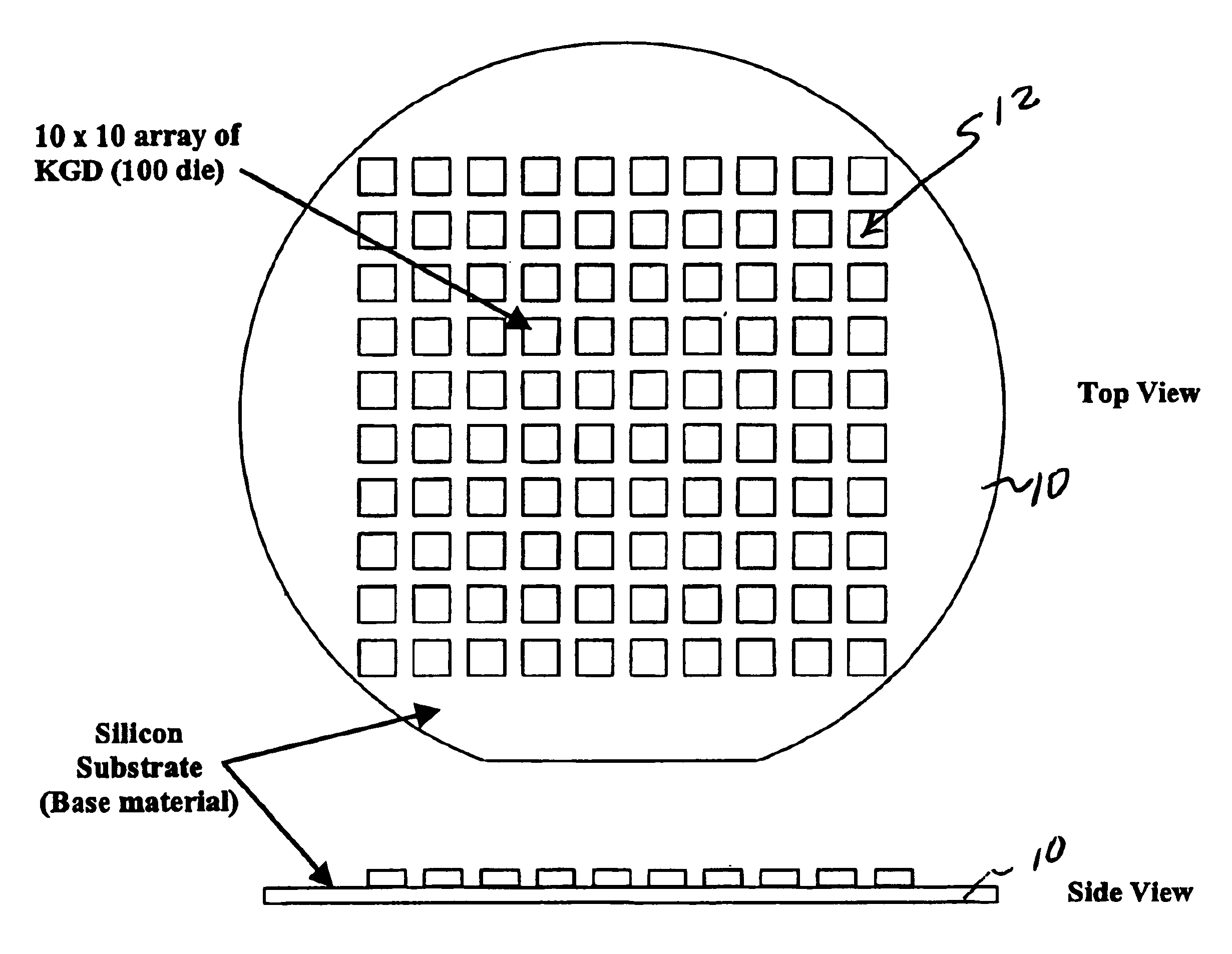
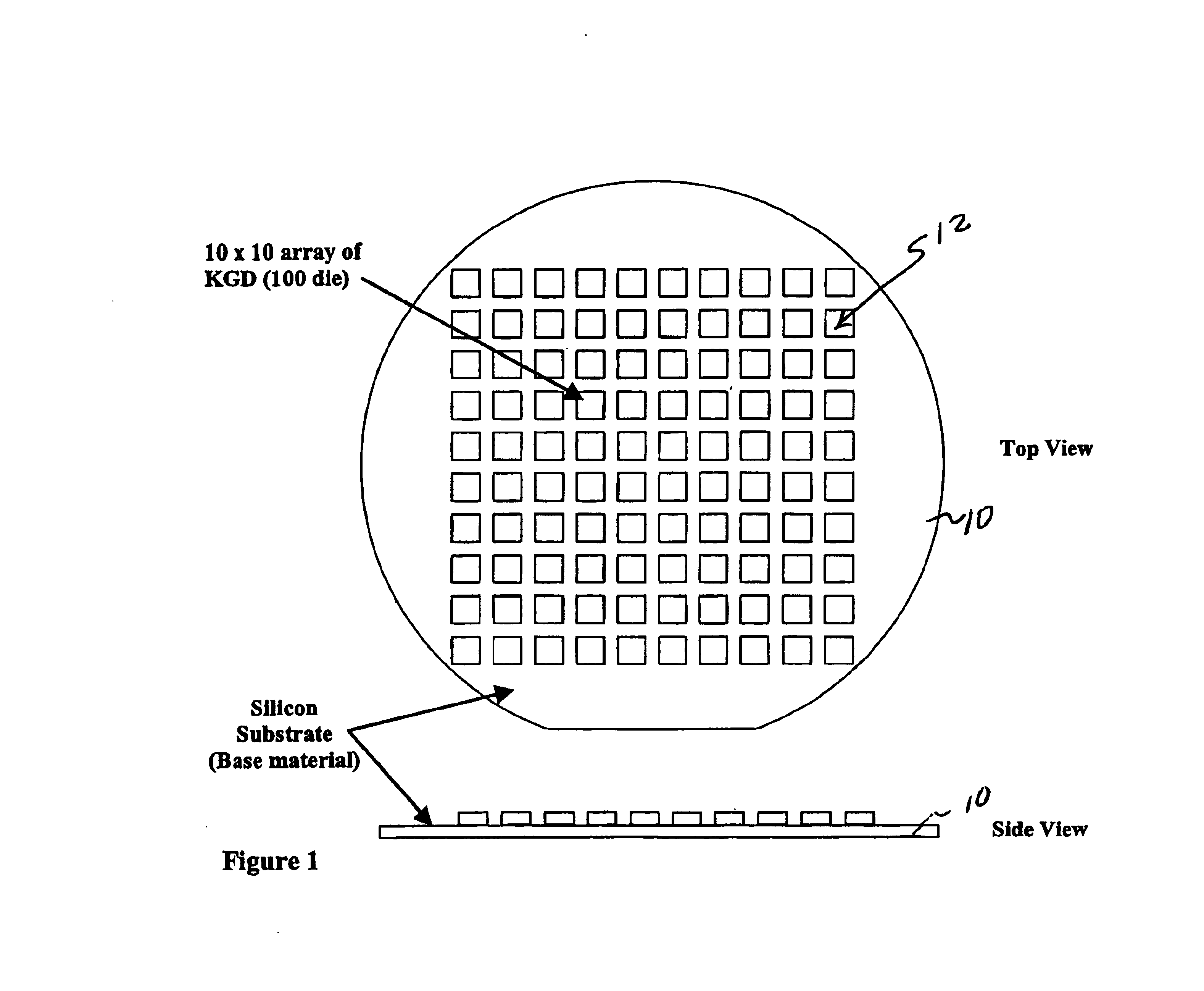
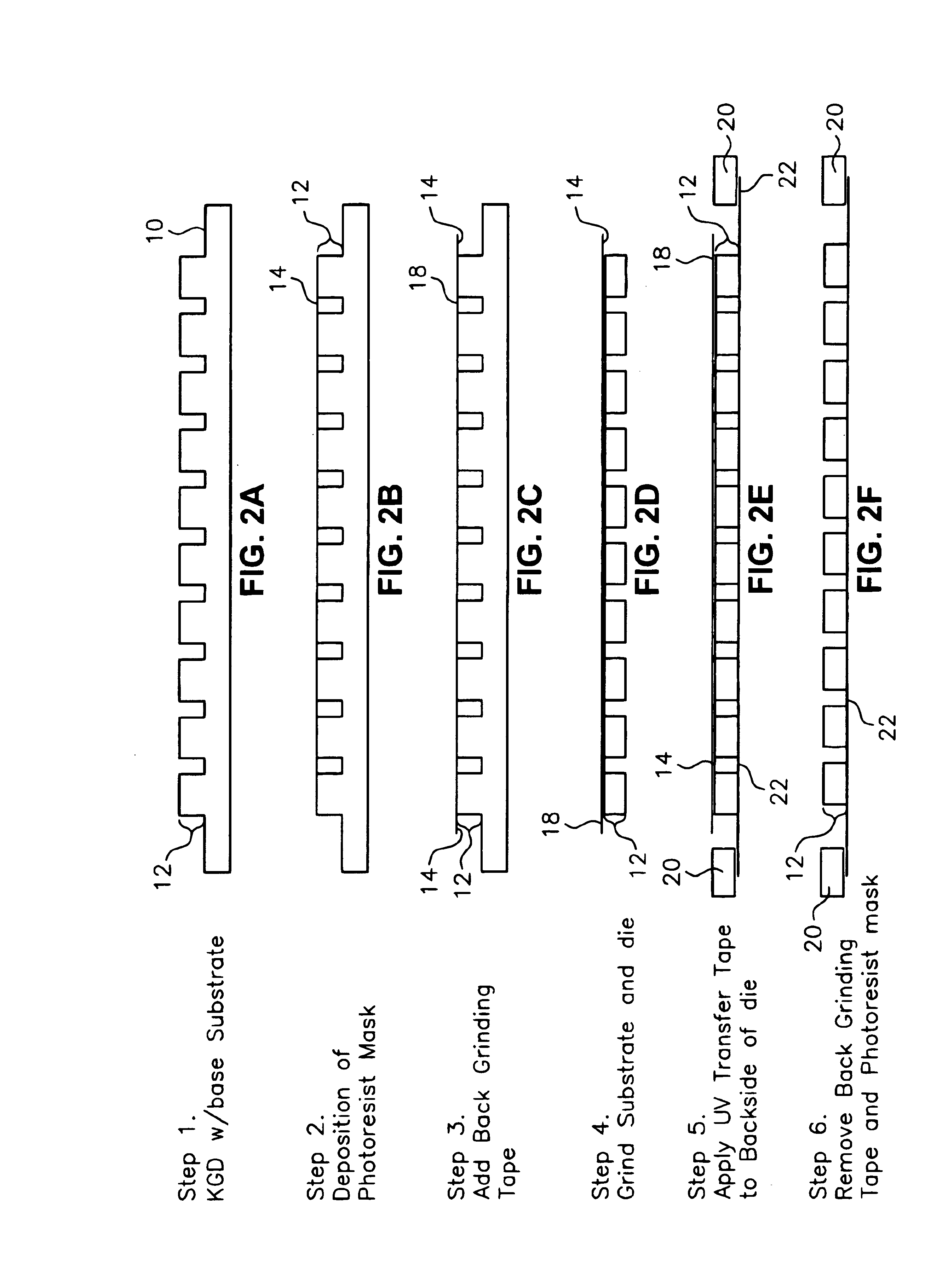
- The method involves depositing a substrate bonding material on a substrate, securing die to the substrate, applying a mask material, grinding to thin the die, using UV transfer tape for removal, and curing the adhesive materials to reduce adhesive strength, allowing for the thinning of die from 26 mils to 5 mils while maintaining mechanical integrity.
Semiconductor Manufacturing Quality Standards and Compliance
Semiconductor manufacturing quality standards play a critical role in governing wafer thinning processes, establishing comprehensive frameworks that ensure consistent die handling performance across different thinning methodologies. International standards such as SEMI specifications, JEDEC guidelines, and ISO quality management systems provide the foundational requirements for evaluating thinning process effectiveness, particularly focusing on dimensional accuracy, surface integrity, and mechanical reliability parameters that directly impact subsequent die handling operations.
Quality compliance in wafer thinning encompasses multiple measurement criteria including total thickness variation (TTV), bow and warp specifications, surface roughness parameters, and edge quality standards. These metrics are particularly crucial when comparing mechanical grinding, chemical mechanical polishing (CMP), and plasma etching approaches, as each method exhibits distinct compliance profiles. Mechanical grinding typically achieves excellent thickness uniformity but may introduce subsurface damage, while CMP delivers superior surface quality at the cost of throughput efficiency.
Regulatory frameworks mandate specific testing protocols for die strength evaluation, including three-point bend tests, die shear strength measurements, and thermal cycling assessments. These standardized testing procedures enable objective comparison of thinning methods by quantifying their impact on die mechanical integrity and handling robustness. Compliance documentation must demonstrate that thinned wafers meet minimum strength requirements while maintaining acceptable yield rates during subsequent assembly processes.
Traceability requirements under quality standards necessitate comprehensive process monitoring and documentation throughout the thinning workflow. This includes real-time thickness measurement systems, defect detection protocols, and statistical process control implementations that ensure consistent quality delivery regardless of the chosen thinning methodology. Advanced metrology systems must comply with calibration standards and measurement uncertainty specifications to provide reliable comparative data.
Quality management systems integration becomes essential when implementing multiple thinning approaches within a single facility, requiring standardized procedures for method selection, process validation, and continuous improvement initiatives. These systems must address risk management protocols, supplier qualification requirements, and customer-specific compliance needs while maintaining operational flexibility across different thinning technologies to optimize die handling characteristics for diverse application requirements.
Quality compliance in wafer thinning encompasses multiple measurement criteria including total thickness variation (TTV), bow and warp specifications, surface roughness parameters, and edge quality standards. These metrics are particularly crucial when comparing mechanical grinding, chemical mechanical polishing (CMP), and plasma etching approaches, as each method exhibits distinct compliance profiles. Mechanical grinding typically achieves excellent thickness uniformity but may introduce subsurface damage, while CMP delivers superior surface quality at the cost of throughput efficiency.
Regulatory frameworks mandate specific testing protocols for die strength evaluation, including three-point bend tests, die shear strength measurements, and thermal cycling assessments. These standardized testing procedures enable objective comparison of thinning methods by quantifying their impact on die mechanical integrity and handling robustness. Compliance documentation must demonstrate that thinned wafers meet minimum strength requirements while maintaining acceptable yield rates during subsequent assembly processes.
Traceability requirements under quality standards necessitate comprehensive process monitoring and documentation throughout the thinning workflow. This includes real-time thickness measurement systems, defect detection protocols, and statistical process control implementations that ensure consistent quality delivery regardless of the chosen thinning methodology. Advanced metrology systems must comply with calibration standards and measurement uncertainty specifications to provide reliable comparative data.
Quality management systems integration becomes essential when implementing multiple thinning approaches within a single facility, requiring standardized procedures for method selection, process validation, and continuous improvement initiatives. These systems must address risk management protocols, supplier qualification requirements, and customer-specific compliance needs while maintaining operational flexibility across different thinning technologies to optimize die handling characteristics for diverse application requirements.
Cost-Benefit Analysis of Different Wafer Thinning Approaches
The economic evaluation of wafer thinning approaches reveals significant variations in both initial investment requirements and long-term operational costs. Mechanical grinding represents the most cost-effective entry point, with equipment costs ranging from $200,000 to $500,000 per system and processing costs of approximately $0.15-0.25 per wafer for standard thickness reduction. The method's mature infrastructure and widespread availability contribute to lower maintenance costs and readily available consumables.
Chemical mechanical polishing systems require substantially higher capital investment, typically $800,000 to $1.5 million per tool, with processing costs escalating to $0.40-0.65 per wafer due to expensive slurries and pad consumption. However, CMP delivers superior surface quality and thickness uniformity, reducing downstream yield losses and potentially offsetting higher processing costs through improved die quality and handling reliability.
Plasma etching technologies present the highest initial investment barrier, with advanced systems costing $1.2-2.5 million. Processing costs vary significantly based on etch chemistry and throughput requirements, ranging from $0.30-0.80 per wafer. The method's precision control capabilities and minimal mechanical stress generation provide substantial benefits for ultra-thin applications below 50 micrometers, where die handling becomes critically challenging.
The benefit analysis demonstrates that grinding's speed advantage translates to higher throughput potential, processing 150-200 wafers per hour compared to CMP's 80-120 wafers per hour. This throughput differential significantly impacts manufacturing economics for high-volume production scenarios. Plasma etching, while slower at 60-100 wafers per hour, offers unmatched process control and damage-free thinning.
Total cost of ownership calculations over five years indicate that mechanical grinding maintains cost leadership for thickness targets above 75 micrometers. CMP becomes economically favorable for applications requiring exceptional surface quality, particularly when downstream assembly yield improvements exceed 2-3%. Plasma etching justifies its premium cost structure primarily in ultra-thin applications where alternative methods face technical limitations or unacceptable die breakage rates during handling operations.
Chemical mechanical polishing systems require substantially higher capital investment, typically $800,000 to $1.5 million per tool, with processing costs escalating to $0.40-0.65 per wafer due to expensive slurries and pad consumption. However, CMP delivers superior surface quality and thickness uniformity, reducing downstream yield losses and potentially offsetting higher processing costs through improved die quality and handling reliability.
Plasma etching technologies present the highest initial investment barrier, with advanced systems costing $1.2-2.5 million. Processing costs vary significantly based on etch chemistry and throughput requirements, ranging from $0.30-0.80 per wafer. The method's precision control capabilities and minimal mechanical stress generation provide substantial benefits for ultra-thin applications below 50 micrometers, where die handling becomes critically challenging.
The benefit analysis demonstrates that grinding's speed advantage translates to higher throughput potential, processing 150-200 wafers per hour compared to CMP's 80-120 wafers per hour. This throughput differential significantly impacts manufacturing economics for high-volume production scenarios. Plasma etching, while slower at 60-100 wafers per hour, offers unmatched process control and damage-free thinning.
Total cost of ownership calculations over five years indicate that mechanical grinding maintains cost leadership for thickness targets above 75 micrometers. CMP becomes economically favorable for applications requiring exceptional surface quality, particularly when downstream assembly yield improvements exceed 2-3%. Plasma etching justifies its premium cost structure primarily in ultra-thin applications where alternative methods face technical limitations or unacceptable die breakage rates during handling operations.
Unlock deeper insights with Patsnap Eureka Quick Research — get a full tech report to explore trends and direct your research. Try now!
Generate Your Research Report Instantly with AI Agent
Supercharge your innovation with Patsnap Eureka AI Agent Platform!