

How to Optimize Adhesion During Wafer Thinning
APR 7, 20269 MIN READ
Generate Your Research Report Instantly with AI Agent
Patsnap Eureka helps you evaluate technical feasibility & market potential.
Wafer Thinning Adhesion Technology Background and Objectives
Wafer thinning has emerged as a critical process in semiconductor manufacturing, driven by the relentless pursuit of miniaturization and enhanced device performance. As electronic devices become increasingly compact and multifunctional, the demand for thinner semiconductor wafers has intensified across various applications, from mobile processors to advanced memory devices. The evolution from thick wafers to ultra-thin substrates represents a fundamental shift in manufacturing paradigms, where traditional mechanical grinding and chemical etching processes must achieve unprecedented precision while maintaining structural integrity.
The historical development of wafer thinning technology traces back to the early 2000s when device thickness requirements began approaching sub-50 micrometer ranges. Initially, manufacturers relied primarily on mechanical back-grinding techniques, which provided adequate results for relatively thick applications. However, as target thicknesses decreased below 25 micrometers, adhesion-related challenges became increasingly prominent, leading to significant yield losses and manufacturing inefficiencies.
Contemporary wafer thinning processes face multifaceted adhesion challenges that directly impact manufacturing success rates. The primary concern centers on maintaining adequate substrate adhesion during aggressive material removal processes while ensuring clean release without residual contamination or mechanical damage. These challenges are particularly acute in advanced packaging applications, where ultra-thin dies must maintain structural integrity throughout complex assembly sequences.
The fundamental objective of optimizing adhesion during wafer thinning encompasses several critical performance targets. Primary goals include achieving consistent adhesion strength across varying substrate materials and surface conditions, minimizing adhesive residue formation that could compromise subsequent processing steps, and maintaining thermal stability throughout temperature cycling inherent in thinning operations. Additionally, the technology must demonstrate compatibility with diverse wafer materials, including silicon, gallium arsenide, and emerging compound semiconductors.
Advanced adhesion optimization also targets enhanced process reliability and repeatability, reducing variability in thinning outcomes that historically plagued high-volume manufacturing environments. The technology evolution aims to establish predictable adhesion characteristics that remain stable across extended processing windows, enabling manufacturers to achieve consistent results regardless of environmental fluctuations or equipment variations.
Furthermore, next-generation adhesion solutions must address emerging requirements for environmentally sustainable processing, incorporating materials and methodologies that minimize waste generation while maintaining superior performance characteristics essential for cutting-edge semiconductor applications.
The historical development of wafer thinning technology traces back to the early 2000s when device thickness requirements began approaching sub-50 micrometer ranges. Initially, manufacturers relied primarily on mechanical back-grinding techniques, which provided adequate results for relatively thick applications. However, as target thicknesses decreased below 25 micrometers, adhesion-related challenges became increasingly prominent, leading to significant yield losses and manufacturing inefficiencies.
Contemporary wafer thinning processes face multifaceted adhesion challenges that directly impact manufacturing success rates. The primary concern centers on maintaining adequate substrate adhesion during aggressive material removal processes while ensuring clean release without residual contamination or mechanical damage. These challenges are particularly acute in advanced packaging applications, where ultra-thin dies must maintain structural integrity throughout complex assembly sequences.
The fundamental objective of optimizing adhesion during wafer thinning encompasses several critical performance targets. Primary goals include achieving consistent adhesion strength across varying substrate materials and surface conditions, minimizing adhesive residue formation that could compromise subsequent processing steps, and maintaining thermal stability throughout temperature cycling inherent in thinning operations. Additionally, the technology must demonstrate compatibility with diverse wafer materials, including silicon, gallium arsenide, and emerging compound semiconductors.
Advanced adhesion optimization also targets enhanced process reliability and repeatability, reducing variability in thinning outcomes that historically plagued high-volume manufacturing environments. The technology evolution aims to establish predictable adhesion characteristics that remain stable across extended processing windows, enabling manufacturers to achieve consistent results regardless of environmental fluctuations or equipment variations.
Furthermore, next-generation adhesion solutions must address emerging requirements for environmentally sustainable processing, incorporating materials and methodologies that minimize waste generation while maintaining superior performance characteristics essential for cutting-edge semiconductor applications.
Market Demand for Advanced Wafer Thinning Solutions
The semiconductor industry's relentless pursuit of miniaturization and performance enhancement has created substantial market demand for advanced wafer thinning solutions. As electronic devices become increasingly compact while requiring higher functionality, manufacturers face mounting pressure to produce thinner wafers without compromising structural integrity or yield rates. This demand is particularly pronounced in mobile device manufacturing, where space constraints drive the need for ultra-thin semiconductor components.
Market drivers extend beyond consumer electronics into automotive, aerospace, and medical device sectors. The automotive industry's transition toward electric vehicles and autonomous driving systems requires sophisticated sensor arrays and power management chips that benefit from optimized wafer thinning processes. These applications demand exceptional reliability standards, making adhesion optimization during thinning a critical quality factor that directly impacts market competitiveness.
The proliferation of Internet of Things devices and wearable technology has intensified demand for cost-effective thinning solutions. Manufacturers seek processes that can achieve consistent adhesion performance across high-volume production runs while maintaining economic viability. Market research indicates growing interest in thinning technologies that can handle diverse substrate materials and varying thickness requirements without extensive process reconfiguration.
Advanced packaging technologies, including through-silicon vias and three-dimensional integrated circuits, represent emerging market segments with specific adhesion requirements. These applications require precise control over wafer handling during thinning operations, as any adhesion-related defects can compromise the entire package assembly. The market increasingly values solutions that provide real-time monitoring and adaptive control capabilities.
Regional market dynamics show concentrated demand in Asia-Pacific manufacturing hubs, where high-volume semiconductor production facilities require scalable thinning solutions. European and North American markets emphasize specialized applications requiring premium adhesion performance, particularly in aerospace and medical device manufacturing. This geographic distribution influences technology development priorities and market entry strategies for advanced wafer thinning equipment suppliers.
Market drivers extend beyond consumer electronics into automotive, aerospace, and medical device sectors. The automotive industry's transition toward electric vehicles and autonomous driving systems requires sophisticated sensor arrays and power management chips that benefit from optimized wafer thinning processes. These applications demand exceptional reliability standards, making adhesion optimization during thinning a critical quality factor that directly impacts market competitiveness.
The proliferation of Internet of Things devices and wearable technology has intensified demand for cost-effective thinning solutions. Manufacturers seek processes that can achieve consistent adhesion performance across high-volume production runs while maintaining economic viability. Market research indicates growing interest in thinning technologies that can handle diverse substrate materials and varying thickness requirements without extensive process reconfiguration.
Advanced packaging technologies, including through-silicon vias and three-dimensional integrated circuits, represent emerging market segments with specific adhesion requirements. These applications require precise control over wafer handling during thinning operations, as any adhesion-related defects can compromise the entire package assembly. The market increasingly values solutions that provide real-time monitoring and adaptive control capabilities.
Regional market dynamics show concentrated demand in Asia-Pacific manufacturing hubs, where high-volume semiconductor production facilities require scalable thinning solutions. European and North American markets emphasize specialized applications requiring premium adhesion performance, particularly in aerospace and medical device manufacturing. This geographic distribution influences technology development priorities and market entry strategies for advanced wafer thinning equipment suppliers.
Current Adhesion Challenges in Wafer Thinning Processes
Wafer thinning processes face significant adhesion-related challenges that directly impact manufacturing yield and device performance. The primary challenge stems from maintaining optimal adhesive bond strength between the wafer and carrier substrate throughout the mechanical grinding and chemical-mechanical polishing stages. Insufficient adhesion leads to wafer detachment, causing catastrophic substrate damage and production losses, while excessive adhesion creates difficulties during subsequent debonding processes.
Temperature-induced adhesion degradation represents a critical constraint in current thinning operations. As wafers undergo grinding processes, frictional heat generation can reach temperatures exceeding 150°C, causing thermal expansion mismatches between silicon wafers and carrier materials. This thermal stress often results in localized adhesive failure, particularly at wafer edges where stress concentration is highest. The challenge intensifies with larger wafer diameters, where thermal gradients become more pronounced across the substrate surface.
Chemical compatibility issues between adhesive materials and process environments pose another significant challenge. Many conventional adhesives exhibit poor resistance to the alkaline slurries used in chemical-mechanical polishing, leading to adhesive swelling, softening, or chemical degradation. This degradation compromises the mechanical integrity of the wafer-carrier bond and introduces contamination risks that can affect subsequent processing steps.
Stress management during ultra-thin wafer processing presents increasingly complex challenges as target thicknesses approach 50 micrometers or less. The mechanical stress induced by grinding forces must be effectively distributed across the wafer surface to prevent micro-crack formation and wafer breakage. Current adhesive systems often lack the necessary stress-dampening properties to protect ultra-thin substrates from mechanical damage during high-precision thinning operations.
Surface preparation and adhesive uniformity control remain persistent challenges affecting adhesion quality. Wafer surface contamination, including organic residues and native oxide variations, creates inconsistent bonding conditions that lead to non-uniform adhesion strength distribution. Additionally, achieving consistent adhesive layer thickness across large wafer surfaces proves difficult with current application methods, resulting in localized stress concentrations and potential failure points during processing.
Temperature-induced adhesion degradation represents a critical constraint in current thinning operations. As wafers undergo grinding processes, frictional heat generation can reach temperatures exceeding 150°C, causing thermal expansion mismatches between silicon wafers and carrier materials. This thermal stress often results in localized adhesive failure, particularly at wafer edges where stress concentration is highest. The challenge intensifies with larger wafer diameters, where thermal gradients become more pronounced across the substrate surface.
Chemical compatibility issues between adhesive materials and process environments pose another significant challenge. Many conventional adhesives exhibit poor resistance to the alkaline slurries used in chemical-mechanical polishing, leading to adhesive swelling, softening, or chemical degradation. This degradation compromises the mechanical integrity of the wafer-carrier bond and introduces contamination risks that can affect subsequent processing steps.
Stress management during ultra-thin wafer processing presents increasingly complex challenges as target thicknesses approach 50 micrometers or less. The mechanical stress induced by grinding forces must be effectively distributed across the wafer surface to prevent micro-crack formation and wafer breakage. Current adhesive systems often lack the necessary stress-dampening properties to protect ultra-thin substrates from mechanical damage during high-precision thinning operations.
Surface preparation and adhesive uniformity control remain persistent challenges affecting adhesion quality. Wafer surface contamination, including organic residues and native oxide variations, creates inconsistent bonding conditions that lead to non-uniform adhesion strength distribution. Additionally, achieving consistent adhesive layer thickness across large wafer surfaces proves difficult with current application methods, resulting in localized stress concentrations and potential failure points during processing.
Current Adhesion Optimization Solutions for Wafer Thinning
01 Adhesive tape and film materials for wafer thinning
Specialized adhesive tapes and films are used during wafer thinning processes to temporarily bond and protect the wafer surface. These materials must provide strong adhesion during grinding or polishing operations while allowing clean removal without residue or damage. The adhesive compositions are designed to withstand mechanical stress and maintain dimensional stability throughout the thinning process.- Temporary bonding adhesives for wafer thinning processes: Specialized temporary bonding adhesives are used to secure wafers to carrier substrates during thinning operations. These adhesives must provide strong adhesion during grinding and polishing while allowing clean debonding after processing. The adhesives are designed to withstand mechanical stress and chemical exposure during thinning, ensuring wafer integrity throughout the process.
- Adhesive tape and film materials for wafer support: Adhesive tapes and films serve as protective layers during wafer thinning, providing mechanical support and preventing damage. These materials feature specific thickness, elasticity, and adhesion properties optimized for semiconductor processing. The tapes must maintain dimensional stability under temperature variations and mechanical stress while enabling residue-free removal.
- Wafer mounting and demounting methods: Various techniques are employed for mounting wafers onto support substrates and subsequent removal after thinning. These methods include thermal release mechanisms, UV-curable adhesives, and mechanical separation processes. The approaches focus on minimizing wafer stress, preventing contamination, and ensuring high yield during the bonding and debonding cycles.
- Surface treatment and preparation for enhanced adhesion: Surface modification techniques are applied to wafers and carrier substrates to improve adhesion quality during thinning. These treatments include plasma processing, chemical cleaning, and primer application to optimize bonding strength. Proper surface preparation ensures uniform adhesion distribution and reduces defects such as voids or delamination during subsequent processing steps.
- Equipment and apparatus for wafer thinning adhesion: Specialized equipment is designed to facilitate wafer bonding and thinning operations with precise control over adhesion parameters. These systems include vacuum chucks, heating stages, and pressure application mechanisms to ensure uniform bonding. The apparatus enables automated handling and processing while maintaining cleanroom standards and minimizing particle contamination.
02 Temporary bonding methods using thermoplastic adhesives
Thermoplastic adhesive materials enable temporary bonding of wafers to carrier substrates during thinning operations. These adhesives can be softened by heat application for bonding and subsequently removed by heating or solvent treatment after processing. The thermoplastic approach provides reversible adhesion suitable for ultra-thin wafer handling and processing.Expand Specific Solutions03 Wafer support systems and carrier plates
Support systems including carrier plates and backing substrates are employed to provide mechanical reinforcement during wafer thinning. These systems use adhesive layers to attach thin wafers to rigid carriers, preventing breakage and enabling handling of ultra-thin semiconductor substrates. The carrier systems facilitate uniform thinning and subsequent processing steps.Expand Specific Solutions04 Adhesive removal and debonding techniques
Various methods are employed to remove adhesives and separate thinned wafers from support structures after processing. Techniques include thermal decomposition, solvent dissolution, mechanical peeling, and laser-assisted debonding. These methods must ensure complete adhesive removal without causing damage to the thinned wafer or leaving contaminating residues that could affect subsequent manufacturing steps.Expand Specific Solutions05 Surface treatment and adhesion enhancement
Surface preparation and treatment methods are applied to improve adhesion between wafers and temporary bonding materials during thinning processes. These treatments may include plasma treatment, chemical modification, or application of primer layers to enhance bonding strength and uniformity. Proper surface treatment ensures reliable adhesion throughout the thinning process while maintaining compatibility with subsequent debonding operations.Expand Specific Solutions
Key Players in Semiconductor Wafer Processing Industry
The wafer thinning adhesion optimization market represents a mature yet evolving segment within the semiconductor manufacturing ecosystem, currently valued at several billion dollars globally and experiencing steady growth driven by advanced packaging demands. The industry has reached technological maturity in traditional applications but faces renewed innovation pressure from emerging requirements like ultra-thin wafers for 5G and IoT devices. Key players demonstrate varying technological capabilities: equipment manufacturers like SUSS MicroTec and Applied Materials provide specialized bonding and debonding systems, while foundries including Taiwan Semiconductor Manufacturing and Semiconductor Manufacturing International implement these solutions at scale. Material suppliers such as Brewer Science, Henkel, and Tokyo Ohka Kogyo compete in developing advanced temporary bonding adhesives and release technologies. Silicon wafer producers like SUMCO and Shin-Etsu Handotai contribute substrate expertise, while companies like Intel and Infineon drive application-specific requirements, creating a competitive landscape characterized by specialized expertise across the manufacturing value chain.
Taiwan Semiconductor Manufacturing Co., Ltd.
Technical Solution: TSMC employs advanced temporary bonding adhesives and carrier wafer technologies for ultra-thin wafer processing down to 25μm thickness. Their approach utilizes thermoplastic adhesives that provide strong bonding during grinding and chemical mechanical polishing processes, while enabling clean debonding at controlled temperatures between 150-200°C. The company has developed proprietary surface treatment methods to enhance adhesion uniformity and reduce wafer warpage during thinning operations. Their process includes plasma activation of carrier wafers and precise adhesive coating thickness control to maintain consistent bonding strength across 300mm wafers.
Strengths: Industry-leading experience in high-volume production, excellent process control and yield optimization. Weaknesses: High capital investment requirements, complex process integration challenges.
Applied Materials South East Asia Pte Ltd.
Technical Solution: Applied Materials offers comprehensive wafer thinning solutions through their Producer platform, featuring advanced temporary bonding systems with specialized adhesive materials. Their technology incorporates real-time monitoring of adhesion strength during the grinding process, utilizing pressure-sensitive adhesives that maintain bond integrity under mechanical stress while allowing controlled release. The system includes automated adhesive dispensing with thickness uniformity of ±2μm across the wafer surface, temperature-controlled bonding chambers, and integrated debonding capabilities using thermal and mechanical release mechanisms. Their approach also includes surface conditioning treatments to optimize adhesion between different substrate materials.
Strengths: Comprehensive equipment solutions, strong R&D capabilities, excellent technical support. Weaknesses: High equipment costs, dependency on proprietary consumables.
Core Patents in Wafer Thinning Adhesion Enhancement
Method of manufacturing laminate and kit of adhesive compositions
PatentPendingUS20240363387A1
Innovation
- A method involving a laminate with a semiconductor substrate, a light-transmissive support substrate, and adhesive layers, where a release layer absorbs light to facilitate easy separation without excessive load on the substrate, using specific thermosetting components and catalysts in the adhesive compositions.


Method of bonding, thinning, and releasing wafer
PatentInactiveUS20090199957A1
Innovation
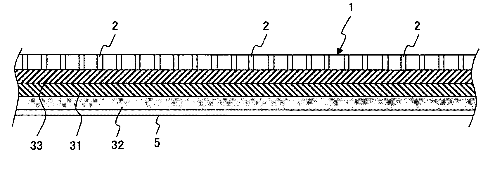
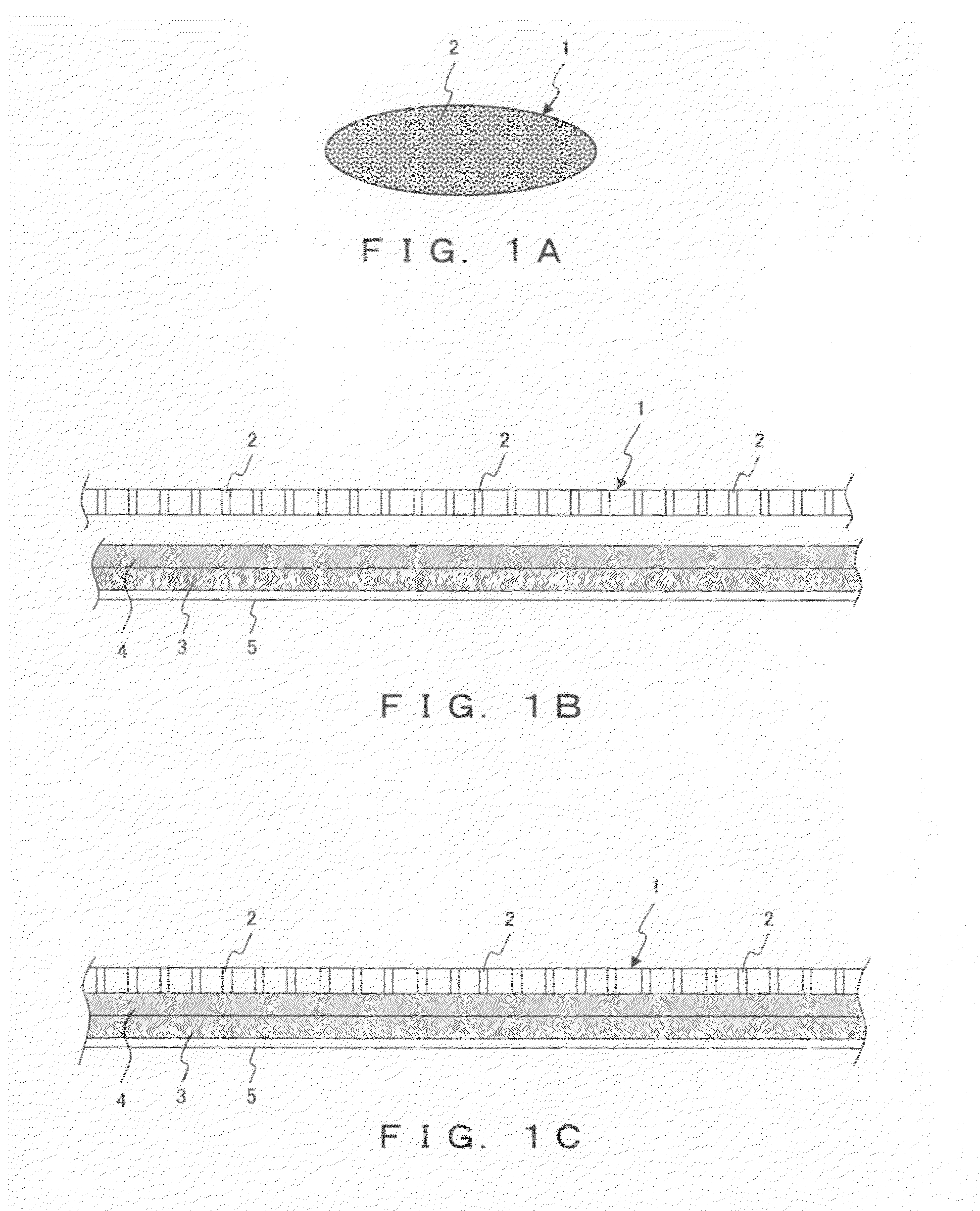
- A method using a combination of soft and hard adhesive agent layers, applied in a three-layer configuration with a hard layer sandwiched between two soft layers, to bond the wafer to a support plate, preventing pattern transfer and ensuring secure bonding without damaging the wafer during grinding and polishing, and using a release agent to dissolve the adhesive layers for safe wafer release.

Environmental Impact of Wafer Thinning Processes
The environmental implications of wafer thinning processes have become increasingly significant as semiconductor manufacturing scales up globally. Traditional mechanical grinding and chemical etching methods generate substantial waste streams, including silicon particulates, chemical slurries, and contaminated process fluids. These byproducts require specialized treatment and disposal protocols, contributing to the overall environmental footprint of semiconductor fabrication facilities.
Chemical mechanical planarization (CMP) processes, commonly employed in wafer thinning, utilize abrasive slurries containing silica particles and various chemical additives. The disposal of spent slurries presents environmental challenges due to their complex composition and potential toxicity. Additionally, the high water consumption required for cleaning and rinsing operations during thinning processes places considerable strain on local water resources, particularly in regions where semiconductor manufacturing is concentrated.
Energy consumption represents another critical environmental consideration. Wafer thinning operations require significant electrical power for equipment operation, including grinding spindles, vacuum systems, and temperature control mechanisms. The carbon footprint associated with this energy usage varies substantially depending on the regional energy mix and facility efficiency measures.
Atmospheric emissions from wafer thinning processes include volatile organic compounds (VOCs) from cleaning solvents and particulate matter from mechanical operations. These emissions necessitate sophisticated air filtration and treatment systems to meet environmental regulations. The implementation of closed-loop systems and advanced filtration technologies has become essential for minimizing atmospheric impact.
Recent regulatory developments have intensified focus on sustainable manufacturing practices within the semiconductor industry. Environmental compliance requirements now mandate comprehensive monitoring of waste streams, energy consumption, and emissions throughout the wafer thinning process. This regulatory pressure has accelerated the adoption of greener alternatives, including waterless cleaning technologies, biodegradable process chemicals, and energy-efficient equipment designs.
The industry's response to environmental concerns has catalyzed innovation in process optimization and waste reduction strategies. Advanced process control systems now enable real-time monitoring of resource consumption, facilitating immediate adjustments to minimize environmental impact while maintaining production quality standards.
Chemical mechanical planarization (CMP) processes, commonly employed in wafer thinning, utilize abrasive slurries containing silica particles and various chemical additives. The disposal of spent slurries presents environmental challenges due to their complex composition and potential toxicity. Additionally, the high water consumption required for cleaning and rinsing operations during thinning processes places considerable strain on local water resources, particularly in regions where semiconductor manufacturing is concentrated.
Energy consumption represents another critical environmental consideration. Wafer thinning operations require significant electrical power for equipment operation, including grinding spindles, vacuum systems, and temperature control mechanisms. The carbon footprint associated with this energy usage varies substantially depending on the regional energy mix and facility efficiency measures.
Atmospheric emissions from wafer thinning processes include volatile organic compounds (VOCs) from cleaning solvents and particulate matter from mechanical operations. These emissions necessitate sophisticated air filtration and treatment systems to meet environmental regulations. The implementation of closed-loop systems and advanced filtration technologies has become essential for minimizing atmospheric impact.
Recent regulatory developments have intensified focus on sustainable manufacturing practices within the semiconductor industry. Environmental compliance requirements now mandate comprehensive monitoring of waste streams, energy consumption, and emissions throughout the wafer thinning process. This regulatory pressure has accelerated the adoption of greener alternatives, including waterless cleaning technologies, biodegradable process chemicals, and energy-efficient equipment designs.
The industry's response to environmental concerns has catalyzed innovation in process optimization and waste reduction strategies. Advanced process control systems now enable real-time monitoring of resource consumption, facilitating immediate adjustments to minimize environmental impact while maintaining production quality standards.
Quality Control Standards for Wafer Thinning Operations
Quality control standards for wafer thinning operations represent a critical framework that ensures consistent adhesion performance throughout the manufacturing process. These standards encompass comprehensive measurement protocols, acceptance criteria, and monitoring procedures that directly impact the optimization of adhesion during wafer processing. The establishment of rigorous quality control measures serves as the foundation for maintaining process reliability and product yield in semiconductor manufacturing.
Dimensional tolerance specifications form the cornerstone of adhesion-related quality control, with thickness uniformity requirements typically maintained within ±2-5 micrometers across the wafer surface. Surface roughness parameters must be controlled to Ra values below 10 nanometers to ensure optimal adhesive contact. Contamination control standards mandate particle density limits below 0.1 particles per square centimeter for particles larger than 0.3 micrometers, as surface contaminants directly compromise adhesive bond strength and uniformity.
Temperature monitoring protocols require continuous tracking of substrate and adhesive temperatures during application and curing phases. Standard operating procedures specify temperature stability within ±2°C during critical adhesion processes, with mandatory calibration of thermal measurement equipment every 30 days. Humidity control standards maintain relative humidity between 45-55% in processing environments to prevent moisture-induced adhesion variability.
Adhesive application quality metrics include coverage uniformity assessments using optical inspection systems with resolution capabilities of 1 micrometer or better. Bubble detection standards require identification and documentation of any air inclusions larger than 50 micrometers in diameter. Bond strength verification procedures mandate periodic destructive testing using standardized peel tests with force measurements accurate to ±0.1 Newton.
Process validation requirements include statistical process control implementation with control charts tracking key adhesion parameters. Capability studies must demonstrate process capability indices (Cpk) greater than 1.33 for critical adhesion characteristics. Documentation standards require comprehensive traceability records linking process parameters to final adhesion performance metrics.
Inspection frequency protocols specify in-line monitoring at predetermined intervals, with 100% inspection for critical dimension measurements and statistical sampling for adhesion strength verification. Non-conformance handling procedures establish clear escalation paths and corrective action requirements when adhesion parameters exceed specified control limits, ensuring immediate process adjustment and quality recovery.
Dimensional tolerance specifications form the cornerstone of adhesion-related quality control, with thickness uniformity requirements typically maintained within ±2-5 micrometers across the wafer surface. Surface roughness parameters must be controlled to Ra values below 10 nanometers to ensure optimal adhesive contact. Contamination control standards mandate particle density limits below 0.1 particles per square centimeter for particles larger than 0.3 micrometers, as surface contaminants directly compromise adhesive bond strength and uniformity.
Temperature monitoring protocols require continuous tracking of substrate and adhesive temperatures during application and curing phases. Standard operating procedures specify temperature stability within ±2°C during critical adhesion processes, with mandatory calibration of thermal measurement equipment every 30 days. Humidity control standards maintain relative humidity between 45-55% in processing environments to prevent moisture-induced adhesion variability.
Adhesive application quality metrics include coverage uniformity assessments using optical inspection systems with resolution capabilities of 1 micrometer or better. Bubble detection standards require identification and documentation of any air inclusions larger than 50 micrometers in diameter. Bond strength verification procedures mandate periodic destructive testing using standardized peel tests with force measurements accurate to ±0.1 Newton.
Process validation requirements include statistical process control implementation with control charts tracking key adhesion parameters. Capability studies must demonstrate process capability indices (Cpk) greater than 1.33 for critical adhesion characteristics. Documentation standards require comprehensive traceability records linking process parameters to final adhesion performance metrics.
Inspection frequency protocols specify in-line monitoring at predetermined intervals, with 100% inspection for critical dimension measurements and statistical sampling for adhesion strength verification. Non-conformance handling procedures establish clear escalation paths and corrective action requirements when adhesion parameters exceed specified control limits, ensuring immediate process adjustment and quality recovery.
Unlock deeper insights with Patsnap Eureka Quick Research — get a full tech report to explore trends and direct your research. Try now!
Generate Your Research Report Instantly with AI Agent
Supercharge your innovation with Patsnap Eureka AI Agent Platform!