

Evaluate Plasma Thinning vs Wet Etching for Performance
APR 7, 20269 MIN READ
Generate Your Research Report Instantly with AI Agent
PatSnap Eureka helps you evaluate technical feasibility & market potential.
Plasma Thinning vs Wet Etching Background and Objectives
Semiconductor manufacturing has undergone continuous evolution since the 1960s, with material removal processes serving as fundamental enablers of device miniaturization and performance enhancement. The transition from purely chemical wet etching methods to plasma-based techniques represents a pivotal technological shift that has shaped modern integrated circuit fabrication. As device geometries have shrunk from micrometers to nanometers, the precision requirements for material removal have intensified exponentially.
Wet etching emerged as the earliest material removal technique in semiconductor processing, utilizing liquid chemical solutions to dissolve target materials through isotropic reactions. This approach dominated early semiconductor manufacturing due to its simplicity, cost-effectiveness, and ability to achieve high selectivity between different materials. However, as feature sizes decreased below 1 micrometer, the inherent limitations of wet etching became increasingly problematic for advanced applications.
Plasma thinning technology developed as a response to the geometric constraints imposed by wet etching processes. By utilizing ionized gases and reactive species in a controlled plasma environment, this dry etching approach enables anisotropic material removal with superior dimensional control. The technology has evolved through multiple generations, incorporating advances in plasma chemistry, reactor design, and process control systems to meet the stringent requirements of sub-nanometer manufacturing nodes.
The primary objective of evaluating plasma thinning versus wet etching performance centers on determining optimal process selection criteria for specific manufacturing applications. This evaluation encompasses multiple performance dimensions including etch rate uniformity, surface roughness control, selectivity ratios, and process-induced damage minimization. Understanding these trade-offs is critical for making informed decisions in advanced semiconductor manufacturing.
Contemporary manufacturing challenges demand comprehensive assessment of both techniques across various substrate materials, device architectures, and production scales. The evaluation must consider not only immediate processing performance but also long-term reliability implications, cost structures, and environmental impact factors. This holistic approach ensures that technology selection aligns with both current production requirements and future scalability needs.
The ultimate goal involves establishing quantitative performance benchmarks that enable data-driven process selection while identifying potential hybrid approaches that leverage the complementary strengths of both plasma thinning and wet etching methodologies.
Market Demand for Advanced Semiconductor Etching Solutions
The semiconductor industry is experiencing unprecedented demand for advanced etching solutions, driven by the continuous miniaturization of electronic devices and the proliferation of emerging technologies. As device geometries shrink below 7nm nodes, traditional manufacturing processes face significant challenges in achieving the precision and selectivity required for next-generation semiconductors. This technological evolution has created a substantial market opportunity for innovative etching solutions that can deliver superior performance while maintaining cost-effectiveness.
The global semiconductor etching equipment market has witnessed robust growth, fueled by increasing demand from multiple sectors including artificial intelligence, 5G communications, automotive electronics, and Internet of Things applications. Memory manufacturers, particularly those producing DRAM and NAND flash devices, represent a significant portion of this demand as they require increasingly sophisticated etching capabilities to achieve higher storage densities and improved performance characteristics.
Advanced logic device manufacturers are driving demand for etching solutions that can handle complex three-dimensional structures and ultra-thin layers with atomic-level precision. The transition to extreme ultraviolet lithography and the adoption of new materials such as high-k dielectrics and metal gates have created additional requirements for etching processes that can maintain critical dimension control while minimizing damage to sensitive device structures.
The market demand is particularly strong for etching solutions that can address specific challenges in plasma thinning and wet etching applications. Plasma thinning processes are increasingly sought after for their ability to achieve uniform material removal across large wafer surfaces, while wet etching solutions remain critical for applications requiring high selectivity and minimal surface damage. Manufacturers are actively seeking technologies that can optimize the trade-offs between these approaches.
Regional demand patterns show significant concentration in Asia-Pacific markets, where major semiconductor foundries and memory manufacturers are expanding production capacity. However, growing demand from automotive and industrial applications is creating new market opportunities in North America and Europe, where specialized semiconductor devices require tailored etching solutions.
The market is also responding to sustainability concerns, with increasing demand for etching processes that reduce chemical consumption, minimize waste generation, and improve energy efficiency. This trend is driving innovation in both plasma and wet etching technologies, as manufacturers seek solutions that can meet environmental regulations while maintaining high performance standards.
Current State and Challenges in Plasma and Wet Etching
Plasma etching has emerged as the dominant technology in advanced semiconductor manufacturing, particularly for sub-10nm nodes where precision and anisotropic profiles are critical. Current plasma systems utilize inductively coupled plasma (ICP) and capacitively coupled plasma (CCP) configurations, achieving etch rates of 100-500 nm/min with aspect ratios exceeding 50:1. However, plasma damage remains a significant concern, with ion bombardment causing lattice defects and charging effects that can degrade device performance by 5-15%.
Wet etching continues to play essential roles in specific applications, particularly for isotropic etching and material selectivity requirements. Modern wet processes achieve selectivity ratios of 1000:1 or higher between different materials, with etch rates ranging from 10-200 nm/min depending on chemistry and temperature. Silicon dioxide wet etching using buffered hydrofluoric acid maintains excellent uniformity across 300mm wafers, with thickness variation below 2%.
The primary challenge in plasma etching centers on controlling plasma-induced damage while maintaining etch precision. Advanced techniques like pulsed plasma and atomic layer etching (ALE) have been developed to minimize damage, but these approaches significantly reduce throughput. Temperature control during plasma processing remains problematic, with substrate heating often exceeding 200°C, potentially affecting temperature-sensitive materials and structures.
Wet etching faces fundamental limitations in pattern fidelity as feature sizes shrink below 20nm. Isotropic nature of wet processes creates undercutting issues, limiting critical dimension control. Additionally, surface tension effects and capillary forces during drying can cause pattern collapse in high-aspect-ratio structures, particularly problematic for advanced memory devices.
Process integration challenges affect both technologies. Plasma etching requires sophisticated endpoint detection and real-time monitoring systems, adding complexity and cost. Wet etching demands precise chemical composition control and waste management, with environmental regulations increasingly restricting certain chemistries. Cross-contamination between different etching steps remains a persistent issue in both approaches.
Equipment scaling represents another significant challenge. Plasma systems require increasingly complex hardware for uniform processing across larger substrates, while maintaining the precise control necessary for advanced nodes. Wet etching equipment must handle more aggressive chemistries while ensuring operator safety and environmental compliance.
Existing Plasma Thinning and Wet Etching Solutions
01 Plasma etching selectivity and uniformity control
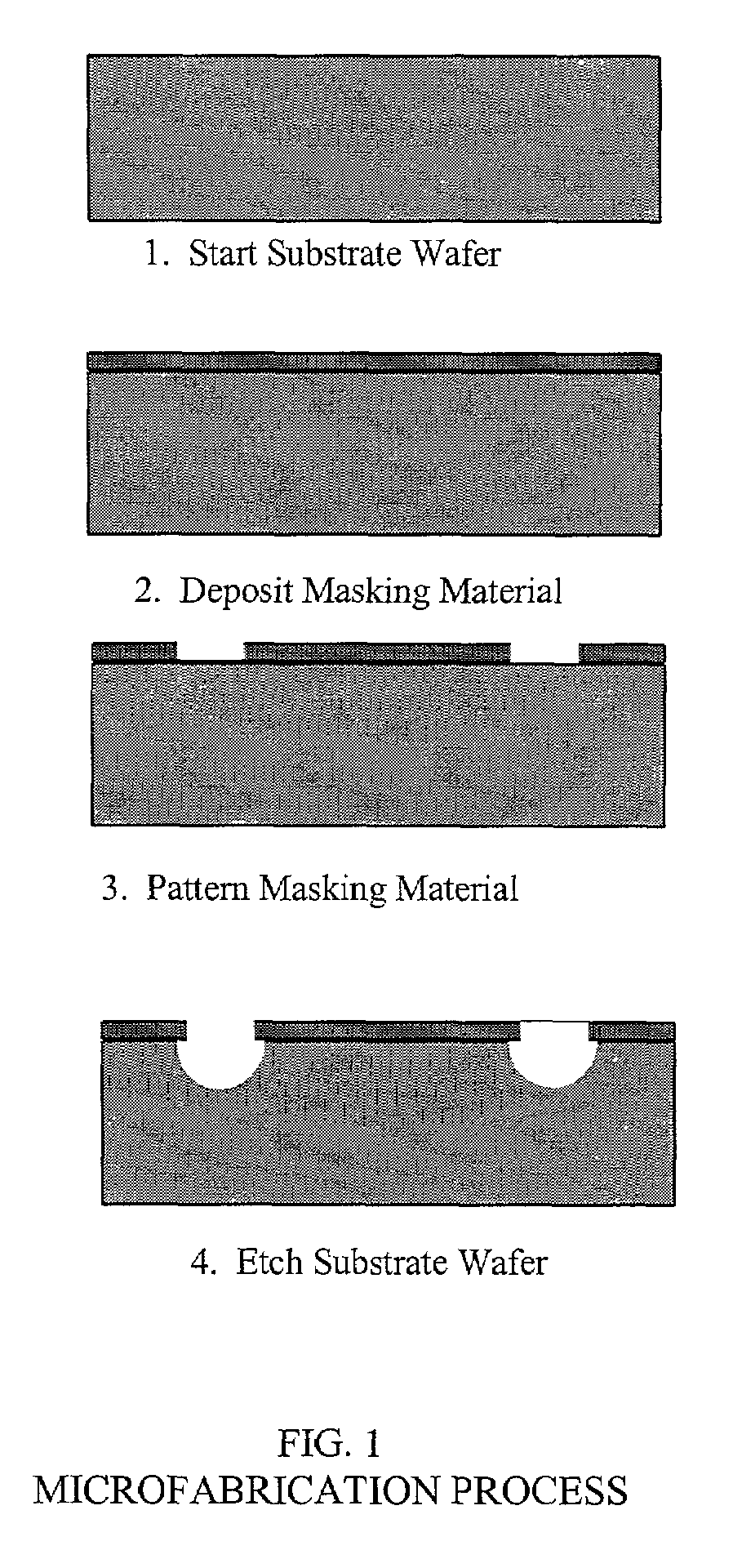
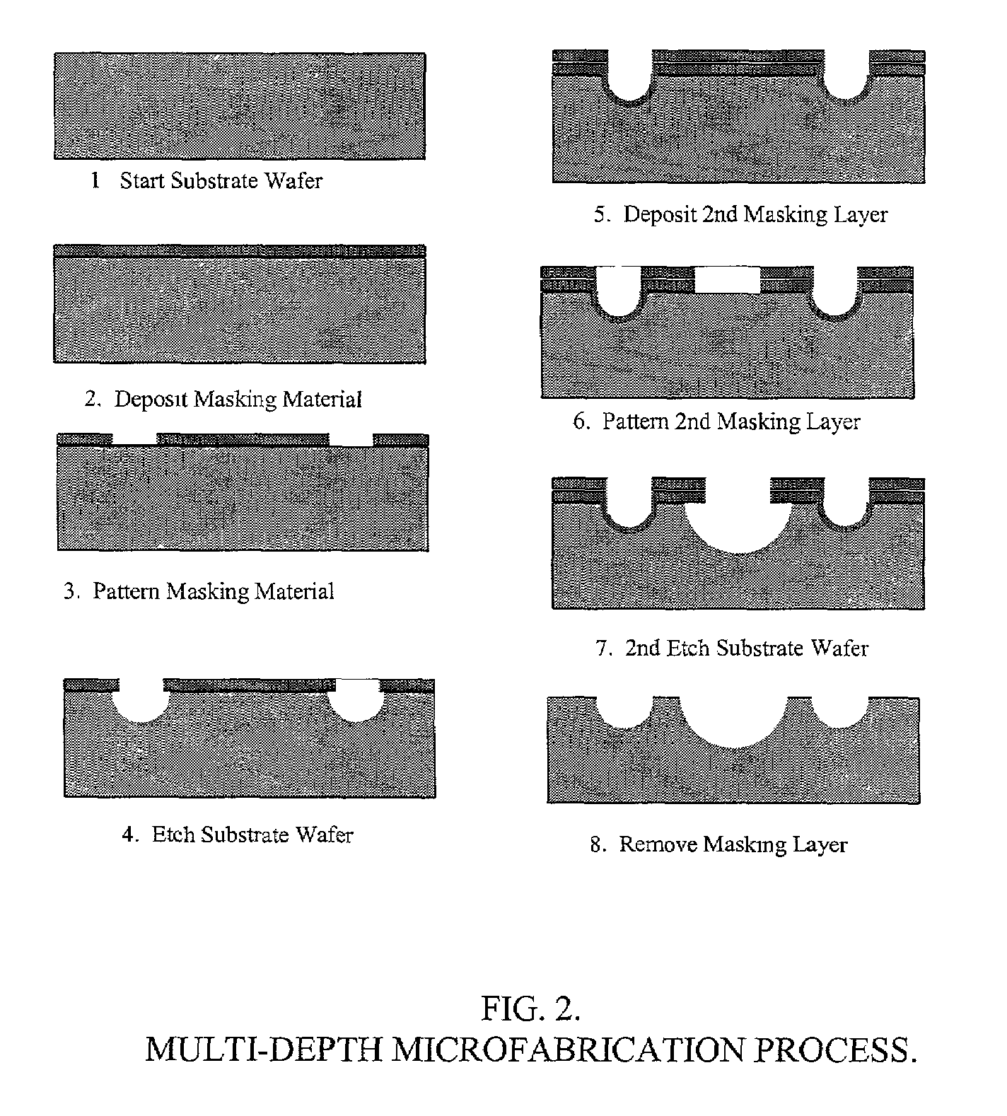
Plasma etching techniques focus on achieving high selectivity between different materials and maintaining uniformity across the substrate. This involves optimizing plasma parameters such as gas composition, pressure, and power to control the etching rate and profile. Advanced plasma systems utilize specific gas mixtures and process conditions to achieve precise material removal while minimizing damage to underlying layers. The selectivity control is crucial for maintaining critical dimensions in semiconductor manufacturing.- Plasma etching selectivity and uniformity control: Plasma etching techniques focus on achieving high selectivity between different material layers while maintaining uniform etching across the substrate surface. This involves optimizing plasma parameters such as gas composition, pressure, and power to control the etching rate and profile. Advanced plasma systems utilize specific gas mixtures and process conditions to achieve anisotropic etching with minimal damage to underlying layers, which is critical for high-aspect-ratio structures in semiconductor manufacturing.
- Wet etching chemical composition and etch rate optimization: Wet etching processes rely on chemical solutions to remove material through isotropic dissolution. The performance depends on the chemical composition of etchants, temperature control, and concentration management to achieve desired etch rates and surface quality. Various chemical formulations are designed to provide specific selectivity ratios between different materials while minimizing surface roughness and contamination. The process is particularly suitable for bulk material removal and cleaning applications.
- Hybrid etching processes combining plasma and wet methods: Combined etching approaches integrate both plasma and wet etching techniques to leverage the advantages of each method. This hybrid strategy typically uses plasma etching for precise pattern definition and anisotropic profiles, followed by wet etching for cleaning, smoothing, or selective material removal. The sequential or alternating application of these methods can improve overall process efficiency, reduce defects, and achieve better dimensional control in complex device structures.
- Damage control and surface quality in etching processes: Both plasma and wet etching methods must address surface damage and quality issues that affect device performance. Plasma etching can cause ion bombardment damage, charging effects, and sidewall roughness, while wet etching may lead to undercutting, surface contamination, and non-uniform material removal. Various techniques are employed to minimize these effects, including optimized process parameters, protective layer deposition, and post-etch treatment procedures to restore surface integrity and ensure reliable device characteristics.
- Equipment design and process monitoring for etching performance: Advanced etching equipment incorporates sophisticated chamber designs, gas delivery systems, and real-time monitoring capabilities to ensure consistent performance. For plasma systems, this includes electrode configuration, magnetic field control, and plasma generation methods. Wet etching equipment focuses on solution circulation, temperature uniformity, and chemical concentration control. In-situ monitoring techniques such as optical emission spectroscopy, interferometry, and endpoint detection enable precise process control and reproducibility across multiple substrates.
02 Wet etching chemical composition and etch rate optimization
Wet etching processes rely on chemical solutions to selectively remove materials through controlled chemical reactions. The performance depends on factors such as etchant composition, temperature, concentration, and immersion time. Different chemical formulations are designed for specific materials to achieve desired etch rates and surface quality. The process enables isotropic etching with good selectivity and is particularly effective for bulk material removal and cleaning applications.Expand Specific Solutions03 Comparative damage and surface quality analysis
The comparison between plasma and wet etching methods reveals distinct differences in surface damage, roughness, and material integrity. Plasma processes can introduce ion bombardment damage and charging effects, while wet etching typically produces smoother surfaces with less physical damage. Evaluation methods include surface morphology analysis, defect inspection, and electrical characterization to assess the impact of each etching technique on device performance and reliability.Expand Specific Solutions04 Anisotropic vs isotropic etching characteristics
Plasma etching generally provides anisotropic profiles with vertical sidewalls due to directional ion bombardment, making it suitable for high-aspect-ratio features and fine pattern transfer. In contrast, wet etching typically exhibits isotropic behavior, etching equally in all directions, which can lead to undercut profiles. The choice between these methods depends on the required feature geometry, critical dimensions, and process integration requirements in device fabrication.Expand Specific Solutions05 Process throughput and cost-effectiveness comparison
The economic and productivity aspects of plasma versus wet etching involve considerations of equipment cost, process time, chemical consumption, and maintenance requirements. Plasma systems typically require higher capital investment but offer better control and automation capabilities. Wet etching processes are generally simpler and more cost-effective for certain applications, with lower equipment costs but potentially higher chemical disposal expenses. Throughput optimization involves balancing batch processing capabilities, cycle times, and yield considerations.Expand Specific Solutions
Key Players in Plasma and Wet Etching Equipment Industry
The plasma thinning versus wet etching technology landscape represents a mature semiconductor processing market experiencing significant evolution driven by advanced node requirements and precision manufacturing demands. The industry is in a consolidation phase where established equipment manufacturers dominate, with market size exceeding $15 billion globally across etch and deposition segments. Technology maturity varies significantly between players, with Applied Materials, Tokyo Electron, and Samsung Electronics leading in advanced plasma processing capabilities, while companies like NAURA Microelectronics and JUSUNG Engineering focus on cost-effective solutions for emerging markets. TSMC and GLOBALFOUNDRIES drive foundry-specific innovations, whereas Plasma-Therm and Veeco Instruments specialize in niche applications. The competitive dynamics show increasing emphasis on atomic-level precision, selectivity improvements, and integration with AI-driven process control, positioning this technology at a critical inflection point between mature wet processing and next-generation plasma solutions.
Applied Materials, Inc.
Technical Solution: Applied Materials offers comprehensive plasma etching solutions through their Centris and Producer platforms, featuring advanced plasma chemistry control and multi-step etching processes. Their plasma thinning technology utilizes precisely controlled ion bombardment and reactive species to achieve uniform material removal with minimal surface damage. The company's wet etching systems incorporate temperature-controlled chemical baths with real-time monitoring capabilities, enabling selective material removal for various semiconductor applications. Their integrated approach combines both plasma and wet etching in sequential processes to optimize performance characteristics including etch rate uniformity, selectivity ratios, and surface roughness control across different substrate materials and device geometries.
Strengths: Industry-leading process control and uniformity, extensive material compatibility, proven scalability for high-volume manufacturing. Weaknesses: Higher capital equipment costs, complex process optimization requirements, longer setup times for new applications.
Tokyo Electron Ltd.
Technical Solution: Tokyo Electron develops advanced plasma etching systems using their proprietary Tactras and Vigus platforms, incorporating innovative plasma source designs and gas delivery systems for precise material removal control. Their plasma thinning approach employs low-damage plasma conditions with optimized ion energy distribution to minimize subsurface defects while maintaining high throughput. The company's wet etching solutions feature advanced chemical delivery systems with precise temperature and concentration control, enabling highly selective etching processes. TEL's comparative analysis shows plasma thinning achieving superior thickness uniformity across large substrates, while wet etching provides better material selectivity for multi-layer structures, with their hybrid processes combining both techniques for optimal performance in advanced semiconductor manufacturing.
Strengths: Excellent process uniformity, strong R&D capabilities, comprehensive process integration solutions. Weaknesses: Limited availability in some regional markets, higher maintenance requirements, steep learning curve for operators.
Core Innovations in Advanced Etching Process Control
Multilayer device for tissue engineering
PatentInactiveUS7371400B2
Innovation
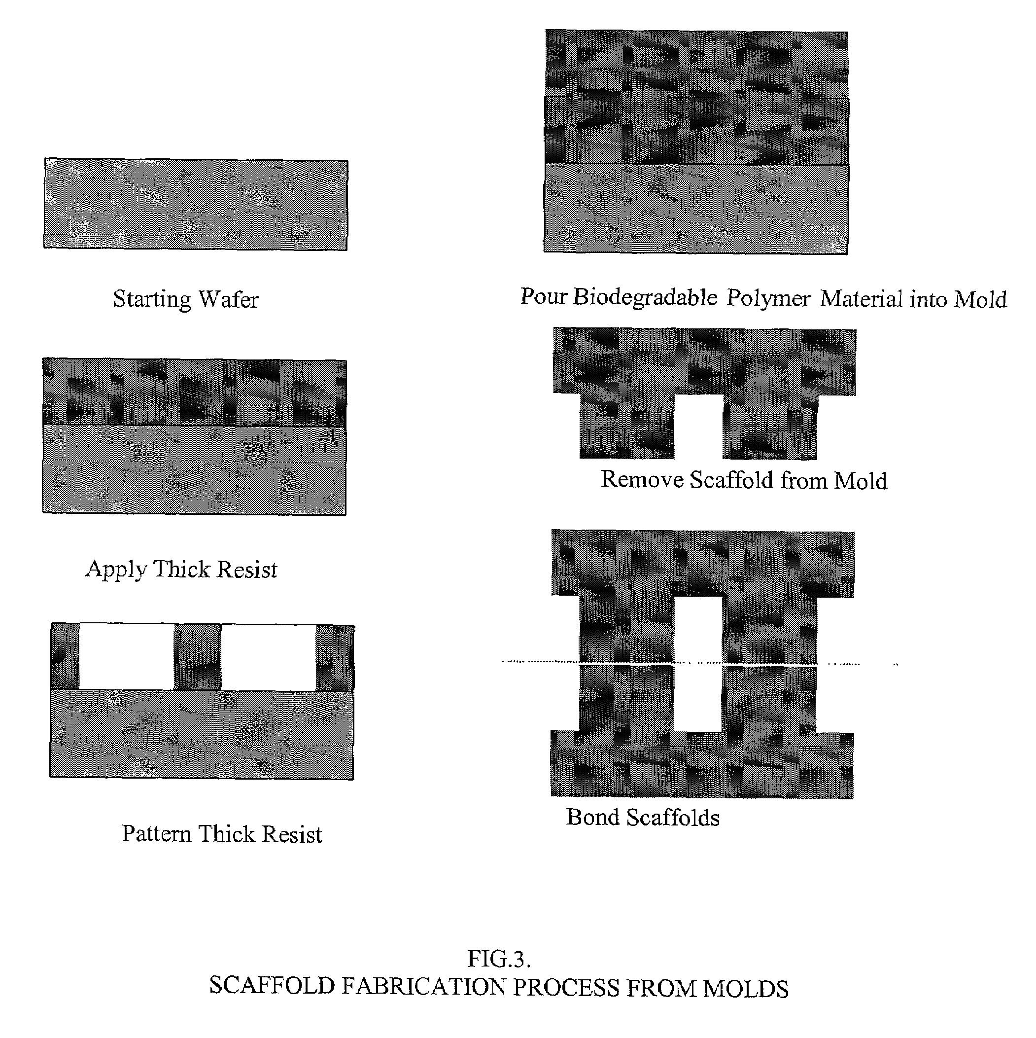
- The development of a method to translate two-dimensional microfabrication technology into the third dimension using high-resolution molding processes to create multilayer devices with connected channels, allowing for the fabrication of biocompatible scaffolds that can be joined to form a vascular network, providing a template for cell adhesion and growth, and enabling the formation of small-diameter blood vessels and other vasculature.

Methods and compositions for selectively etching metal films and structures
PatentInactiveUS20050053869A1
Innovation
- The use of high-concentration chelating agents, tailored to specific metals, in wet chemistry etching processes to form soluble metal complexes, preventing redeposition and preserving other films, with concentrations ranging from 0.5-5 moles/liter and tailored to target specific metals or alloys.


Environmental Impact and Sustainability in Etching Processes
The environmental implications of plasma thinning versus wet etching processes represent a critical consideration in semiconductor manufacturing sustainability. Both technologies present distinct environmental profiles that significantly impact industrial ecological footprints and regulatory compliance strategies.
Plasma thinning processes demonstrate superior environmental performance through reduced chemical consumption and waste generation. These dry etching methods eliminate the need for hazardous liquid chemicals, substantially decreasing toxic waste streams and associated disposal costs. The primary environmental concern involves energy consumption, as plasma generation requires significant electrical power, contributing to carbon emissions depending on energy source composition.
Wet etching processes present more complex environmental challenges due to extensive chemical usage. Traditional wet etching employs acids, bases, and organic solvents that generate substantial liquid waste requiring specialized treatment facilities. Chemical procurement, storage, and disposal create comprehensive environmental management requirements, including air emission controls and groundwater protection measures.
Water consumption patterns differ significantly between these approaches. Wet etching demands substantial deionized water for rinsing operations, creating large volumes of contaminated wastewater requiring treatment before discharge. Plasma processes minimize water usage, primarily requiring cooling systems and occasional cleaning operations, resulting in dramatically reduced water footprint.
Waste stream characteristics vary considerably between technologies. Plasma etching generates gaseous byproducts that can be effectively captured and neutralized through scrubber systems, while wet etching produces liquid waste containing dissolved metals and organic compounds requiring complex treatment processes. The recyclability potential of plasma process waste streams generally exceeds that of wet etching residues.
Regulatory compliance frameworks increasingly favor plasma technologies due to stricter environmental standards. Emerging sustainability metrics emphasize lifecycle assessments, carbon footprint reduction, and circular economy principles, positioning plasma thinning as the more environmentally sustainable option despite higher initial energy requirements.
Future sustainability trends indicate growing preference for plasma-based processes as renewable energy adoption reduces their carbon intensity, while wet etching faces increasing regulatory pressure and disposal cost escalation.
Cost-Performance Trade-offs in Etching Method Selection
The selection between plasma thinning and wet etching technologies involves complex cost-performance considerations that significantly impact manufacturing economics and product quality outcomes. Initial capital expenditure analysis reveals that plasma etching systems typically require substantially higher upfront investments, with advanced inductively coupled plasma (ICP) systems costing between $2-5 million compared to wet etching stations ranging from $200,000-800,000. However, this initial cost differential must be evaluated against long-term operational efficiency and throughput capabilities.
Operational cost structures demonstrate contrasting patterns between these methodologies. Plasma etching incurs higher energy consumption due to RF power requirements and vacuum system maintenance, with typical power consumption ranging from 5-15 kW per chamber. Conversely, wet etching processes consume significantly less energy but generate substantial chemical waste requiring specialized disposal protocols, adding $50-200 per wafer batch in waste management costs depending on chemistry complexity and environmental regulations.
Throughput analysis reveals plasma etching's superior batch processing capabilities, enabling simultaneous processing of 25-300 wafers depending on chamber configuration, compared to wet etching's typical 25-50 wafer capacity. This translates to plasma etching achieving 20-40 wafers per hour throughput versus wet etching's 15-25 wafers per hour, directly impacting per-unit processing costs in high-volume manufacturing scenarios.
Quality-related cost implications present another critical dimension. Plasma etching's superior dimensional control and reduced defect rates translate to higher yield percentages, typically achieving 95-99% yield compared to wet etching's 85-95% range for critical dimension applications. This yield differential significantly impacts overall manufacturing economics, particularly for high-value semiconductor devices where single wafer costs can exceed $1,000.
Process flexibility considerations affect long-term cost optimization strategies. Plasma systems offer greater adaptability for multiple process recipes and materials, reducing the need for dedicated equipment investments when product portfolios expand. Wet etching systems, while less flexible, provide cost-effective solutions for specific applications with established process requirements and lower precision demands.
Maintenance cost analysis shows plasma systems requiring specialized technical expertise and expensive consumables including RF generators, vacuum pumps, and chamber components, typically accounting for 15-25% of annual operational costs. Wet etching maintenance focuses primarily on chemical delivery systems and bath management, representing 8-15% of operational expenses but requiring more frequent chemical replenishment cycles.
Unlock deeper insights with PatSnap Eureka Quick Research — get a full tech report to explore trends and direct your research. Try now!
Generate Your Research Report Instantly with AI Agent
Supercharge your innovation with PatSnap Eureka AI Agent Platform!