

Optimize Wafer Thinning for Thin Die Applications
APR 7, 20269 MIN READ
Generate Your Research Report Instantly with AI Agent
PatSnap Eureka helps you evaluate technical feasibility & market potential.
Wafer Thinning Technology Background and Objectives
Wafer thinning technology has emerged as a critical enabler in the semiconductor industry's relentless pursuit of miniaturization and enhanced performance. This process involves the systematic reduction of silicon wafer thickness from the standard 725-775 micrometers to ultra-thin dimensions, often below 50 micrometers for advanced applications. The technology has evolved from a specialized manufacturing step to an essential requirement for modern electronic devices demanding compact form factors and superior electrical characteristics.
The historical development of wafer thinning can be traced back to the early 1990s when the semiconductor industry first recognized the need for thinner substrates to improve device performance. Initially driven by packaging constraints in mobile devices, the technology has undergone significant transformation through mechanical grinding, chemical-mechanical polishing, and plasma etching methodologies. Each evolutionary phase has addressed specific challenges related to surface quality, thickness uniformity, and structural integrity.
Current market demands for thin die applications span across diverse sectors including mobile communications, automotive electronics, medical implants, and Internet of Things devices. The proliferation of 5G technology, artificial intelligence processors, and wearable electronics has intensified the requirement for ultra-thin semiconductor components that can deliver high performance while occupying minimal space.
The primary technical objectives of optimized wafer thinning encompass achieving precise thickness control with variations below ±2 micrometers across entire wafer surfaces. Surface roughness minimization to sub-nanometer levels represents another critical goal, ensuring optimal die strength and electrical performance. Additionally, the technology aims to eliminate subsurface damage that could compromise device reliability and yield.
Advanced thinning processes must also address thermal management challenges inherent in thin die applications. Reduced substrate thickness affects heat dissipation characteristics, necessitating innovative approaches to maintain operational stability. The integration of stress management techniques during thinning operations has become paramount to prevent wafer warpage and cracking that could render devices unusable.
Future technological trajectories focus on developing hybrid thinning methodologies that combine multiple processing techniques to achieve unprecedented thickness uniformity and surface quality. The incorporation of real-time monitoring systems and artificial intelligence-driven process control represents the next frontier in wafer thinning optimization, promising enhanced yield rates and reduced manufacturing costs while meeting the increasingly stringent requirements of next-generation thin die applications.
Market Demand for Ultra-Thin Die Applications
The semiconductor industry is experiencing unprecedented demand for ultra-thin die applications, driven by the relentless pursuit of miniaturization and enhanced performance across multiple technology sectors. Consumer electronics manufacturers are pushing the boundaries of device thickness to create sleeker smartphones, tablets, and wearables that meet evolving aesthetic and functional requirements. The transition toward foldable displays and flexible electronics has intensified the need for dies with thickness measurements below 50 micrometers, creating new technical challenges for wafer thinning processes.
Mobile device manufacturers represent the largest market segment demanding ultra-thin die solutions. Advanced packaging technologies such as system-in-package and multi-chip modules require extremely thin semiconductor components to achieve optimal space utilization and thermal management. The automotive electronics sector is simultaneously driving demand through the proliferation of advanced driver assistance systems and electric vehicle power management units, where space constraints necessitate ultra-thin semiconductor solutions.
The Internet of Things ecosystem has emerged as a significant growth driver for ultra-thin die applications. Sensor nodes, RFID tags, and embedded processors require minimal form factors to enable seamless integration into everyday objects and industrial equipment. Medical device manufacturers are increasingly adopting ultra-thin semiconductor solutions for implantable devices, continuous monitoring systems, and minimally invasive diagnostic equipment, where biocompatibility and size constraints are paramount.
Memory and storage applications constitute another substantial market segment. Three-dimensional NAND flash memory architectures and high-bandwidth memory configurations demand precise wafer thinning to achieve optimal stacking densities and thermal characteristics. The emergence of neuromorphic computing and artificial intelligence accelerators is creating additional demand for specialized ultra-thin die configurations that enable efficient parallel processing architectures.
Market growth is further accelerated by the expansion of 5G infrastructure and edge computing applications. Base station components, millimeter-wave transceivers, and distributed processing units require ultra-thin semiconductor solutions to meet stringent size and weight specifications. The convergence of these diverse application domains is creating a robust and sustained demand environment that challenges traditional wafer thinning methodologies and drives continuous innovation in semiconductor manufacturing processes.
Current Wafer Thinning Challenges and Technical Barriers
Wafer thinning for thin die applications faces significant technical challenges that limit manufacturing efficiency and yield rates. The primary constraint lies in mechanical stress management during the grinding and polishing processes. As wafer thickness reduces below 50 micrometers, the substrate becomes increasingly susceptible to warpage, cracking, and breakage due to inherent material stress and thermal expansion mismatches.
Process control precision represents another critical barrier in ultra-thin wafer manufacturing. Conventional grinding techniques struggle to maintain uniform thickness distribution across large wafer surfaces, particularly for 300mm substrates. Thickness variation tolerance requirements of ±2 micrometers become extremely difficult to achieve using standard backgrinding equipment, leading to significant yield losses and performance inconsistencies in final devices.
Surface quality degradation emerges as wafers approach extreme thinness levels. Subsurface damage from mechanical grinding processes penetrates deeper relative to the remaining wafer thickness, compromising electrical performance and reliability. Traditional chemical-mechanical polishing methods require extended processing times to remove damaged layers, further increasing the risk of wafer breakage and contamination.
Handling and transportation challenges multiply exponentially with reduced wafer thickness. Standard vacuum chuck systems and robotic handling equipment designed for conventional wafer thicknesses become inadequate for ultra-thin substrates. Wafer bow and stress-induced deformation make reliable wafer transfer between processing stations increasingly problematic, resulting in higher breakage rates and reduced manufacturing throughput.
Temperature management during thinning processes presents additional complexity. Heat generation from grinding operations can cause thermal stress concentrations that exceed the mechanical strength limits of thin wafers. Cooling system optimization becomes critical to prevent thermal damage while maintaining processing efficiency and surface quality standards.
Metrology and inspection limitations constrain process optimization efforts. Existing thickness measurement systems lack sufficient resolution and accuracy for ultra-thin wafer applications. Real-time monitoring capabilities remain inadequate for detecting early signs of stress accumulation or surface defects that could lead to catastrophic wafer failure during subsequent processing steps.
Chemical compatibility issues arise when implementing wet processing steps for stress relief and surface preparation. Etchant penetration rates and selectivity characteristics change significantly with reduced wafer thickness, requiring extensive process requalification and optimization to maintain consistent results across different wafer lots and processing conditions.
Existing Wafer Thinning Process Solutions
01 Grinding and polishing methods for wafer thinning
Wafer thinning can be achieved through mechanical grinding and polishing processes that remove material from the backside of the wafer. These methods involve using abrasive materials and grinding wheels to reduce wafer thickness to desired specifications. The process typically includes rough grinding followed by fine grinding and polishing stages to achieve the target thickness while maintaining surface quality and minimizing damage to the wafer structure.- Grinding and polishing methods for wafer thinning: Various grinding and polishing techniques are employed to reduce wafer thickness to desired specifications. These methods involve mechanical abrasion using grinding wheels with specific grit sizes, followed by fine polishing processes to achieve smooth surfaces and precise thickness control. The processes may include multiple stages with progressively finer abrasives to minimize surface damage and achieve uniform thickness across the wafer.
- Measurement and monitoring systems for thickness control: Advanced measurement technologies are integrated into wafer thinning processes to ensure precise thickness control. These systems utilize optical, capacitive, or ultrasonic sensors to continuously monitor wafer thickness during processing. Real-time feedback mechanisms allow for automatic adjustment of processing parameters to maintain target thickness specifications and improve yield rates.
- Chemical mechanical planarization for ultra-thin wafers: Chemical mechanical planarization combines chemical etching with mechanical polishing to achieve ultra-thin wafer specifications. This hybrid approach allows for controlled material removal while maintaining excellent surface quality and thickness uniformity. The process is particularly effective for achieving very thin wafers required in advanced semiconductor applications, with careful control of slurry composition and processing conditions.
- Protective backing and support structures during thinning: Temporary bonding and support structures are utilized to protect thin wafers during processing and handling. These methods involve applying protective layers or mounting wafers on carrier substrates before thinning operations. The support structures prevent wafer breakage and warping during aggressive thinning processes, and can be removed after processing is complete without damaging the thinned wafer.
- Stress management and defect reduction techniques: Specialized techniques are employed to manage mechanical stress and reduce defects introduced during wafer thinning. These approaches include controlled grinding rates, optimized cooling systems, and post-thinning annealing processes. Stress relief methods help prevent wafer cracking and warping, while defect reduction techniques minimize subsurface damage that could affect device performance and reliability.
02 Thickness measurement and monitoring during thinning process
Accurate measurement and real-time monitoring of wafer thickness during the thinning process is critical for achieving precise thickness control. Various measurement techniques including optical, capacitive, and contact-based methods can be employed to monitor thickness reduction. These measurement systems enable feedback control to ensure uniform thickness across the wafer and prevent over-thinning or damage to the device structures.Expand Specific Solutions03 Chemical mechanical polishing for ultra-thin wafers
Chemical mechanical polishing combines chemical etching with mechanical abrasion to achieve ultra-thin wafer thickness with superior surface quality. This technique is particularly effective for achieving very thin wafers while maintaining excellent surface flatness and minimizing subsurface damage. The process parameters including slurry composition, polishing pressure, and rotation speed can be optimized to control the thinning rate and final thickness.Expand Specific Solutions04 Wafer support and handling systems for thin wafer processing
Specialized support and handling systems are essential for processing ultra-thin wafers to prevent breakage and warping during thinning operations. These systems may include temporary bonding to carrier substrates, vacuum chuck designs, and protective tape applications. The support mechanisms enable safe handling and processing of thin wafers while maintaining thickness uniformity and preventing mechanical stress that could cause wafer cracking or deformation.Expand Specific Solutions05 Plasma etching and dry etching techniques for wafer thinning
Plasma-based and dry etching methods provide alternative approaches to wafer thinning that can achieve precise thickness control without mechanical stress. These techniques use reactive gases and plasma to remove material from the wafer backside through chemical reactions. Dry etching methods offer advantages in terms of process cleanliness, reduced surface damage, and the ability to achieve very uniform thickness across the wafer surface, particularly for advanced semiconductor applications.Expand Specific Solutions
Major Players in Wafer Thinning Equipment Industry
The wafer thinning optimization market for thin die applications represents a mature yet rapidly evolving sector driven by increasing demand for miniaturized electronics and advanced packaging solutions. The industry has reached a consolidation phase where established players dominate through technological expertise and manufacturing scale. Market size continues expanding, particularly in automotive, mobile, and IoT segments requiring ultra-thin semiconductor devices. Technology maturity varies significantly across the competitive landscape. Leading foundries like Taiwan Semiconductor Manufacturing Co. and Semiconductor Manufacturing International demonstrate advanced capabilities, while equipment manufacturers such as Applied Materials, Tokyo Seimitsu, and SPTS Technologies provide specialized thinning solutions. Material suppliers including Shin-Etsu Handotai and Dow Silicones Corp. offer critical substrate and processing materials. Assembly and test service providers like Siliconware Precision Industries and Tianshui Huatian Technology focus on post-thinning packaging optimization, creating a comprehensive ecosystem supporting thin die manufacturing requirements.
Taiwan Semiconductor Manufacturing Co., Ltd.
Technical Solution: TSMC has developed advanced wafer thinning technologies for ultra-thin die applications, utilizing precision grinding and chemical mechanical polishing (CMP) processes. Their approach combines backside grinding with stress relief techniques to achieve wafer thickness down to 25-50 micrometers while maintaining structural integrity. The company employs specialized carrier wafer bonding and debonding processes using temporary adhesives that can withstand high-temperature processing. TSMC's thinning process includes multiple stages: initial rough grinding, fine grinding with diamond wheels, stress relief annealing, and final polishing to achieve mirror-like surface finish with minimal subsurface damage.
Strengths: Industry-leading precision and yield rates, extensive experience with high-volume manufacturing, advanced process control systems. Weaknesses: High capital investment requirements, complex process integration challenges for new materials.
SPTS Technologies Ltd.
Technical Solution: SPTS Technologies provides advanced plasma processing solutions for wafer thinning applications, utilizing deep reactive ion etching (DRIE) and plasma-enhanced chemical vapor deposition (PECVD) technologies. Their approach enables precise thickness control through plasma-based material removal processes that minimize mechanical stress and subsurface damage compared to traditional grinding methods. The company's systems feature advanced endpoint detection capabilities using optical interferometry and mass spectrometry to achieve precise thickness targets. Their technology supports both silicon and compound semiconductor substrates, with specialized process recipes optimized for different material systems and device requirements.
Strengths: Precise plasma-based processing capabilities, minimal mechanical stress introduction, excellent uniformity control across wafer surface. Weaknesses: Lower throughput compared to mechanical grinding methods, higher operating costs due to plasma processing requirements.
Core Patents in Advanced Wafer Thinning Methods
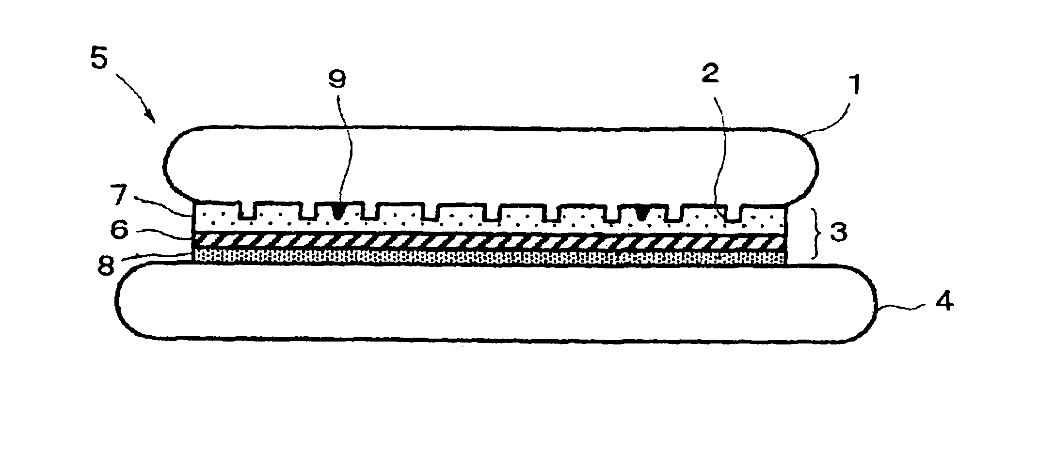
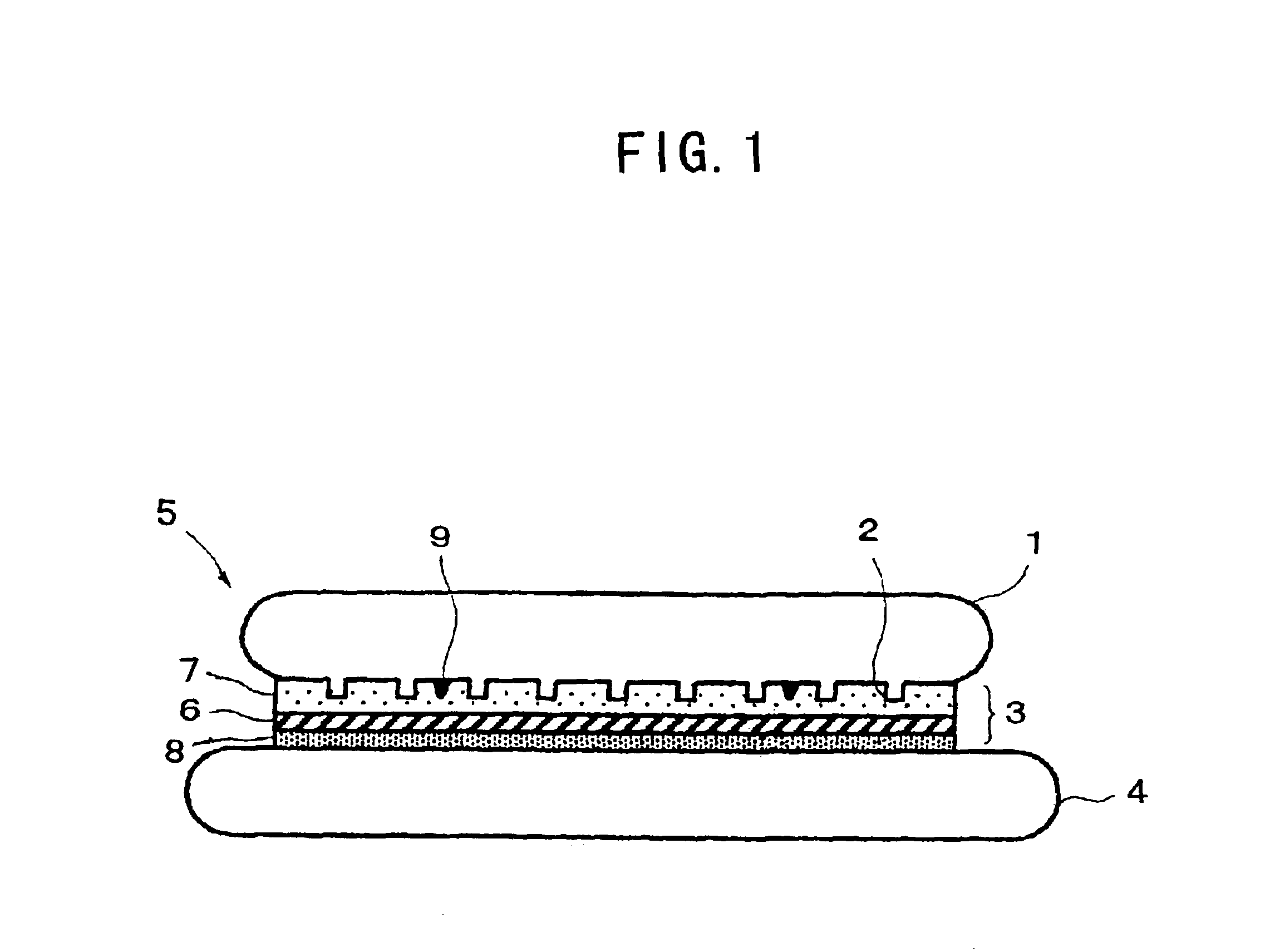
Semiconductor wafer thinning method, and thin semiconductor wafer
PatentInactiveUS6930023B2
Innovation
- A method involving adhering the semiconductor wafer to a support via an adhesive layer, specifically a thermal release double-sided adhesive sheet, and grinding the back surface to achieve thinner wafers without breakage, allowing for easy release and minimizing stress through matching thermal expansion coefficients and using a larger adhesive surface for secure adhesion.

Die thinning processes and structures
PatentWO2009124243A2
Innovation
- A method involving a film to adhere and thin microelectronic dies simultaneously with high accuracy and uniformity, using lapping and chemical-mechanical polishing techniques, and applying pressure through specific centers of pressure to achieve a final thickness of less than 40 μm with minimal variation across dies.


Equipment Safety Standards for Wafer Processing
Equipment safety standards for wafer processing in thin die applications represent a critical framework that governs the operational parameters and protective measures necessary during wafer thinning operations. These standards encompass comprehensive guidelines that address both personnel safety and equipment integrity throughout the mechanical grinding, chemical etching, and plasma processing stages commonly employed in achieving ultra-thin wafer geometries.
The semiconductor industry has established rigorous safety protocols specifically tailored to wafer thinning equipment, with particular emphasis on chemical handling procedures. Given that many thinning processes utilize corrosive chemicals such as hydrofluoric acid, potassium hydroxide, and various organic solvents, equipment must incorporate advanced containment systems, emergency shutdown mechanisms, and real-time monitoring capabilities to prevent exposure incidents and environmental contamination.
Mechanical safety considerations for grinding and polishing equipment include mandatory implementation of vibration dampening systems, precision chuck mechanisms with fail-safe features, and automated thickness monitoring to prevent catastrophic wafer breakage. Equipment operators must adhere to strict protocols regarding protective equipment usage, including specialized gloves, eye protection, and respiratory safety measures when working with particulate-generating processes.
Electrical safety standards mandate comprehensive grounding systems, surge protection, and isolation protocols for high-voltage plasma processing equipment commonly used in advanced thinning applications. Emergency power cutoff systems must be strategically positioned and regularly tested to ensure immediate equipment shutdown capability during anomalous conditions.
Environmental safety protocols require sophisticated exhaust and filtration systems capable of managing both chemical vapors and particulate matter generated during thinning operations. Equipment must incorporate redundant monitoring systems for air quality, chemical concentration levels, and waste stream management to maintain compliance with occupational health standards.
Regular calibration and maintenance schedules form integral components of safety compliance, ensuring that protective systems maintain optimal performance throughout extended production cycles. Documentation requirements mandate detailed logging of safety system performance, incident reporting, and preventive maintenance activities to support continuous improvement initiatives and regulatory compliance verification.
Cost-Benefit Analysis of Thinning Technologies
The economic evaluation of wafer thinning technologies reveals significant variations in cost structures and return on investment across different methodologies. Mechanical grinding, while representing the most established approach, demonstrates relatively low initial capital requirements but faces escalating operational costs due to consumable replacement and maintenance needs. The cost per wafer processed through mechanical grinding typically ranges from $0.15 to $0.35, depending on target thickness and substrate material properties.
Chemical mechanical polishing (CMP) presents a higher upfront investment profile, with equipment costs exceeding mechanical grinding by 40-60%. However, CMP delivers superior surface quality and thickness uniformity, translating to reduced downstream processing costs and improved yield rates. The enhanced die strength achieved through CMP processing can justify the premium, particularly for applications requiring ultra-thin profiles below 50 micrometers.
Plasma-based thinning technologies command the highest initial investment, with system costs often exceeding $2 million per tool. Despite this substantial capital requirement, plasma thinning offers exceptional process control and minimal mechanical stress introduction. The technology demonstrates compelling economics for high-volume production scenarios, where the cost per wafer can decrease to $0.20-$0.30 while maintaining superior quality metrics.
The total cost of ownership analysis reveals that hybrid approaches combining multiple thinning technologies often optimize overall economics. Sequential processing using mechanical grinding for bulk material removal followed by CMP for final finishing can reduce total processing costs by 15-25% compared to single-technology approaches while maintaining quality standards.
Yield impact considerations significantly influence the cost-benefit equation. Advanced thinning technologies that minimize subsurface damage and stress-induced defects can improve overall die yield by 5-12%, effectively offsetting higher processing costs through increased saleable output. This yield enhancement becomes particularly valuable for high-performance applications where die selling prices exceed $10 per unit.
Energy consumption patterns vary substantially across thinning technologies, with plasma-based systems typically consuming 2-3 times more power than mechanical alternatives. However, reduced processing time and improved throughput often compensate for higher energy costs, resulting in comparable or superior cost-per-wafer metrics for high-volume manufacturing environments.
Unlock deeper insights with PatSnap Eureka Quick Research — get a full tech report to explore trends and direct your research. Try now!
Generate Your Research Report Instantly with AI Agent
Supercharge your innovation with PatSnap Eureka AI Agent Platform!