

Wafer Thinning vs Bonding: Ensuring Structural Integrity
APR 7, 20269 MIN READ
Generate Your Research Report Instantly with AI Agent
Patsnap Eureka helps you evaluate technical feasibility & market potential.
Wafer Processing Technology Background and Objectives
Wafer processing technology has undergone remarkable evolution since the inception of semiconductor manufacturing in the 1950s. Initially, wafer thicknesses ranged from 500-700 micrometers, primarily driven by mechanical handling requirements rather than electrical performance considerations. The industry's relentless pursuit of miniaturization and enhanced functionality has fundamentally transformed wafer processing paradigms, particularly in the domains of wafer thinning and bonding technologies.
The emergence of three-dimensional integration and advanced packaging solutions has positioned wafer thinning as a critical enabler for modern semiconductor devices. Traditional grinding and chemical-mechanical polishing techniques have evolved to achieve ultra-thin wafer profiles below 50 micrometers, enabling significant reductions in device footprint and thermal resistance. Concurrently, wafer bonding technologies have matured from simple adhesive-based approaches to sophisticated direct bonding, fusion bonding, and hybrid bonding methodologies.
Contemporary semiconductor applications demand unprecedented levels of structural integrity while maintaining electrical performance and thermal management capabilities. The convergence of Internet of Things devices, 5G communications, artificial intelligence processors, and automotive electronics has created stringent requirements for wafer-level packaging solutions that can withstand mechanical stress, thermal cycling, and environmental challenges.
The primary objective of advancing wafer thinning and bonding technologies centers on achieving optimal balance between structural robustness and functional performance. This encompasses developing methodologies to minimize stress-induced defects during thinning processes, enhancing interfacial adhesion strength in bonded structures, and establishing predictive models for long-term reliability assessment. Critical focus areas include mitigating warpage and bow effects, controlling surface roughness parameters, and optimizing bonding interface characteristics.
Furthermore, the integration of heterogeneous materials through advanced bonding techniques presents both opportunities and challenges for maintaining structural integrity. The objective extends beyond mere mechanical stability to encompass thermal expansion matching, electrical isolation requirements, and compatibility with downstream assembly processes. Success in these endeavors will enable next-generation semiconductor devices with enhanced performance density while ensuring manufacturing yield and long-term reliability in demanding operational environments.
The emergence of three-dimensional integration and advanced packaging solutions has positioned wafer thinning as a critical enabler for modern semiconductor devices. Traditional grinding and chemical-mechanical polishing techniques have evolved to achieve ultra-thin wafer profiles below 50 micrometers, enabling significant reductions in device footprint and thermal resistance. Concurrently, wafer bonding technologies have matured from simple adhesive-based approaches to sophisticated direct bonding, fusion bonding, and hybrid bonding methodologies.
Contemporary semiconductor applications demand unprecedented levels of structural integrity while maintaining electrical performance and thermal management capabilities. The convergence of Internet of Things devices, 5G communications, artificial intelligence processors, and automotive electronics has created stringent requirements for wafer-level packaging solutions that can withstand mechanical stress, thermal cycling, and environmental challenges.
The primary objective of advancing wafer thinning and bonding technologies centers on achieving optimal balance between structural robustness and functional performance. This encompasses developing methodologies to minimize stress-induced defects during thinning processes, enhancing interfacial adhesion strength in bonded structures, and establishing predictive models for long-term reliability assessment. Critical focus areas include mitigating warpage and bow effects, controlling surface roughness parameters, and optimizing bonding interface characteristics.
Furthermore, the integration of heterogeneous materials through advanced bonding techniques presents both opportunities and challenges for maintaining structural integrity. The objective extends beyond mere mechanical stability to encompass thermal expansion matching, electrical isolation requirements, and compatibility with downstream assembly processes. Success in these endeavors will enable next-generation semiconductor devices with enhanced performance density while ensuring manufacturing yield and long-term reliability in demanding operational environments.
Market Demand for Advanced Wafer Processing Solutions
The semiconductor industry is experiencing unprecedented demand for advanced wafer processing solutions, driven by the relentless miniaturization of electronic devices and the proliferation of emerging technologies. Consumer electronics manufacturers are pushing for thinner, lighter devices with enhanced performance capabilities, creating substantial market pressure for innovative wafer thinning and bonding technologies that maintain structural integrity while achieving ultra-thin form factors.
The automotive sector represents a rapidly expanding market segment, particularly with the accelerated adoption of electric vehicles and autonomous driving systems. These applications require robust semiconductor components that can withstand harsh environmental conditions while maintaining reliability. Advanced wafer processing solutions that ensure structural integrity during thinning and bonding operations are becoming critical enablers for automotive-grade semiconductor manufacturing.
Data centers and cloud computing infrastructure are generating significant demand for high-performance computing chips with improved thermal management characteristics. Wafer thinning technologies enable better heat dissipation while advanced bonding techniques facilitate the creation of three-dimensional integrated circuits, addressing the growing need for computational density and energy efficiency in server applications.
The Internet of Things ecosystem is driving demand for miniaturized sensors and wireless communication devices that require ultra-thin semiconductor components. These applications necessitate precise wafer processing techniques that can achieve extreme thickness reduction without compromising mechanical strength or electrical performance, creating substantial market opportunities for specialized processing equipment and materials.
Mobile device manufacturers continue to demand thinner semiconductor packages to enable sleeker product designs while maintaining functionality. Advanced wafer processing solutions that combine effective thinning with reliable bonding are essential for producing the compact, high-performance chips required for smartphones, tablets, and wearable devices.
Medical device applications are emerging as a significant growth driver, requiring biocompatible semiconductor components with exceptional reliability standards. The demand for implantable devices and portable medical equipment is creating new market segments for wafer processing technologies that can deliver both miniaturization and long-term structural stability.
The market demand is further amplified by the transition to advanced packaging technologies, including system-in-package and wafer-level packaging solutions, which require sophisticated processing capabilities to maintain structural integrity throughout the manufacturing process while achieving the desired performance characteristics.
The automotive sector represents a rapidly expanding market segment, particularly with the accelerated adoption of electric vehicles and autonomous driving systems. These applications require robust semiconductor components that can withstand harsh environmental conditions while maintaining reliability. Advanced wafer processing solutions that ensure structural integrity during thinning and bonding operations are becoming critical enablers for automotive-grade semiconductor manufacturing.
Data centers and cloud computing infrastructure are generating significant demand for high-performance computing chips with improved thermal management characteristics. Wafer thinning technologies enable better heat dissipation while advanced bonding techniques facilitate the creation of three-dimensional integrated circuits, addressing the growing need for computational density and energy efficiency in server applications.
The Internet of Things ecosystem is driving demand for miniaturized sensors and wireless communication devices that require ultra-thin semiconductor components. These applications necessitate precise wafer processing techniques that can achieve extreme thickness reduction without compromising mechanical strength or electrical performance, creating substantial market opportunities for specialized processing equipment and materials.
Mobile device manufacturers continue to demand thinner semiconductor packages to enable sleeker product designs while maintaining functionality. Advanced wafer processing solutions that combine effective thinning with reliable bonding are essential for producing the compact, high-performance chips required for smartphones, tablets, and wearable devices.
Medical device applications are emerging as a significant growth driver, requiring biocompatible semiconductor components with exceptional reliability standards. The demand for implantable devices and portable medical equipment is creating new market segments for wafer processing technologies that can deliver both miniaturization and long-term structural stability.
The market demand is further amplified by the transition to advanced packaging technologies, including system-in-package and wafer-level packaging solutions, which require sophisticated processing capabilities to maintain structural integrity throughout the manufacturing process while achieving the desired performance characteristics.
Current Wafer Thinning and Bonding Technology Status
The semiconductor industry currently employs several established wafer thinning technologies, each with distinct advantages and limitations. Mechanical grinding remains the most widely adopted method, utilizing diamond wheels to reduce wafer thickness from standard 725μm to target specifications ranging from 50μm to 300μm. This process achieves high throughput and cost-effectiveness but introduces subsurface damage that requires subsequent removal through chemical-mechanical polishing or wet etching.
Chemical-mechanical polishing has evolved as a critical complementary technology, combining mechanical abrasion with chemical reactions to achieve ultra-smooth surfaces with minimal subsurface damage. Advanced CMP systems now incorporate real-time thickness monitoring and adaptive pressure control, enabling thickness uniformity within ±2μm across 300mm wafers. However, the process remains time-intensive and generates significant chemical waste.
Plasma etching technologies have gained prominence for precision applications, offering damage-free thinning with excellent thickness control. Deep reactive ion etching systems can achieve sub-micron thickness uniformity while maintaining crystal structure integrity. The technology excels in processing compound semiconductors and advanced materials but faces limitations in throughput and cost-effectiveness for high-volume manufacturing.
Wafer bonding technologies have simultaneously advanced to address structural integrity challenges. Direct bonding techniques, including hydrophilic and hydrophobic bonding, enable room-temperature initial bonding followed by high-temperature annealing to achieve covalent bonds with interface strengths exceeding 2 J/m². These methods require exceptional surface preparation with roughness below 0.5nm RMS and particle contamination under 0.1 particles/cm².
Adhesive bonding solutions have diversified to include thermoplastic, thermoset, and UV-curable polymers optimized for semiconductor applications. Advanced adhesive formulations now offer thermal stability up to 400°C, low outgassing properties, and coefficient of thermal expansion matching silicon substrates. Temporary bonding systems using thermoplastic materials enable ultra-thin wafer processing with subsequent debonding at controlled temperatures.
Anodic bonding continues serving specialized applications requiring hermetic sealing, particularly in MEMS devices. The technology achieves bond strengths comparable to silicon bulk strength while maintaining electrical isolation. Recent developments include low-temperature anodic bonding processes operating below 300°C to accommodate temperature-sensitive devices.
Integration challenges persist in combining thinning and bonding processes while maintaining structural integrity. Current manufacturing flows require careful optimization of process sequences, with particular attention to stress management during thermal cycling and handling procedures for ultra-thin substrates below 100μm thickness.
Chemical-mechanical polishing has evolved as a critical complementary technology, combining mechanical abrasion with chemical reactions to achieve ultra-smooth surfaces with minimal subsurface damage. Advanced CMP systems now incorporate real-time thickness monitoring and adaptive pressure control, enabling thickness uniformity within ±2μm across 300mm wafers. However, the process remains time-intensive and generates significant chemical waste.
Plasma etching technologies have gained prominence for precision applications, offering damage-free thinning with excellent thickness control. Deep reactive ion etching systems can achieve sub-micron thickness uniformity while maintaining crystal structure integrity. The technology excels in processing compound semiconductors and advanced materials but faces limitations in throughput and cost-effectiveness for high-volume manufacturing.
Wafer bonding technologies have simultaneously advanced to address structural integrity challenges. Direct bonding techniques, including hydrophilic and hydrophobic bonding, enable room-temperature initial bonding followed by high-temperature annealing to achieve covalent bonds with interface strengths exceeding 2 J/m². These methods require exceptional surface preparation with roughness below 0.5nm RMS and particle contamination under 0.1 particles/cm².
Adhesive bonding solutions have diversified to include thermoplastic, thermoset, and UV-curable polymers optimized for semiconductor applications. Advanced adhesive formulations now offer thermal stability up to 400°C, low outgassing properties, and coefficient of thermal expansion matching silicon substrates. Temporary bonding systems using thermoplastic materials enable ultra-thin wafer processing with subsequent debonding at controlled temperatures.
Anodic bonding continues serving specialized applications requiring hermetic sealing, particularly in MEMS devices. The technology achieves bond strengths comparable to silicon bulk strength while maintaining electrical isolation. Recent developments include low-temperature anodic bonding processes operating below 300°C to accommodate temperature-sensitive devices.
Integration challenges persist in combining thinning and bonding processes while maintaining structural integrity. Current manufacturing flows require careful optimization of process sequences, with particular attention to stress management during thermal cycling and handling procedures for ultra-thin substrates below 100μm thickness.
Current Structural Integrity Solutions in Wafer Processing
01 Wafer thinning methods and grinding techniques
Various mechanical and chemical-mechanical grinding methods are employed to thin semiconductor wafers to desired thicknesses while maintaining surface quality and minimizing subsurface damage. These techniques include back-grinding processes, polishing methods, and controlled material removal strategies that preserve wafer flatness and reduce stress. Advanced grinding equipment and process parameters are optimized to achieve uniform thickness distribution across the wafer surface.- Wafer thinning methods and grinding techniques: Various mechanical and chemical-mechanical grinding methods are employed to thin semiconductor wafers to desired thicknesses while maintaining surface quality and minimizing damage. These techniques include back-grinding processes, polishing methods, and controlled material removal strategies that preserve wafer integrity during the thinning process. Advanced grinding equipment and process parameters are optimized to achieve uniform thickness distribution and reduce subsurface damage that could compromise structural integrity.
- Temporary bonding and debonding technologies: Temporary bonding techniques are utilized to provide mechanical support to thinned wafers during processing and handling. These methods involve applying temporary adhesive materials or bonding layers to carrier substrates, which can be subsequently removed without damaging the thinned wafer. The bonding materials and processes are designed to withstand processing temperatures and mechanical stresses while allowing clean separation after processing is complete.
- Permanent wafer bonding and stacking structures: Permanent bonding technologies enable the creation of multi-layer semiconductor structures through wafer-to-wafer bonding. These techniques include direct bonding, adhesive bonding, and fusion bonding methods that create strong mechanical and electrical connections between thinned wafers. The bonding processes are optimized to minimize voids, ensure uniform bond strength across the wafer surface, and maintain alignment precision for three-dimensional integrated circuit applications.
- Stress management and crack prevention: Techniques for managing mechanical stress and preventing crack formation during wafer thinning and bonding processes are critical for maintaining structural integrity. These approaches include stress-relief layer incorporation, thermal treatment optimization, and edge protection methods. Process parameters such as temperature ramping rates, pressure application, and material selection are carefully controlled to minimize thermal and mechanical stress that could lead to wafer warpage, cracking, or delamination.
- Quality inspection and structural integrity testing: Non-destructive testing methods and quality control procedures are implemented to assess the structural integrity of thinned and bonded wafers. These techniques include acoustic microscopy, infrared inspection, and mechanical strength testing to detect defects such as voids, delamination, and microcracks. Real-time monitoring systems and post-process inspection protocols ensure that bonded structures meet reliability requirements and can withstand subsequent processing steps and operational conditions.
02 Temporary bonding and debonding technologies
Temporary bonding materials and processes are utilized to provide mechanical support during wafer thinning operations. These technologies involve applying adhesive layers or bonding agents to attach the device wafer to a carrier substrate, enabling safe handling and processing of ultra-thin wafers. Subsequent debonding methods allow for clean separation without damaging the thinned wafer or leaving residues that could affect device performance.Expand Specific Solutions03 Permanent wafer bonding and stacking structures
Permanent bonding techniques are employed to create multi-layer semiconductor structures with strong interfacial adhesion. These methods include direct bonding, adhesive bonding, and fusion bonding processes that ensure reliable mechanical and electrical connections between wafers. The bonding processes are designed to minimize voids, achieve high bond strength, and maintain alignment accuracy for three-dimensional integration applications.Expand Specific Solutions04 Stress management and structural reinforcement
Techniques for managing mechanical stress and preventing wafer warpage or cracking during thinning and bonding processes are critical for maintaining structural integrity. These approaches include stress-relief layers, reinforcement structures, and optimized thermal treatment schedules that compensate for coefficient of thermal expansion mismatches. Design considerations for edge protection and support structures help prevent edge chipping and improve overall mechanical stability.Expand Specific Solutions05 Quality inspection and defect detection methods
Non-destructive testing and inspection techniques are employed to evaluate bond quality, detect voids, measure thickness uniformity, and identify structural defects in thinned and bonded wafers. These methods include acoustic microscopy, infrared imaging, and optical inspection systems that assess interfacial integrity and mechanical properties. Real-time monitoring during processing enables early detection of potential failures and process optimization.Expand Specific Solutions
Major Players in Wafer Processing Equipment Industry
The wafer thinning and bonding technology sector represents a mature yet rapidly evolving segment within the semiconductor manufacturing ecosystem, driven by increasing demands for advanced packaging and 3D integration solutions. The market demonstrates substantial growth potential, particularly in automotive, mobile, and high-performance computing applications requiring enhanced structural integrity and miniaturization. Technology maturity varies significantly across the competitive landscape, with established foundries like Taiwan Semiconductor Manufacturing Co., GLOBALFOUNDRIES, and United Microelectronics Corp. leading in advanced process capabilities and volume production. Chinese players including SMIC, ChangXin Memory Technologies, and National Center for Advanced Packaging are aggressively developing capabilities to compete in this space. Specialized equipment providers such as EV Group and SÜSS MicroTec maintain technological leadership in bonding and lithography solutions, while materials companies like Soitec and Brewer Science drive innovation in substrate technologies and process materials, creating a highly competitive environment with diverse technological approaches.
Taiwan Semiconductor Manufacturing Co., Ltd.
Technical Solution: TSMC employs advanced wafer thinning technologies including backgrinding and chemical mechanical polishing (CMP) to achieve ultra-thin wafers down to 25-50 micrometers for 3D packaging applications. Their CoWoS (Chip-on-Wafer-on-Substrate) technology integrates precise wafer thinning with advanced bonding techniques using temporary bonding carriers and debonding processes. The company utilizes stress management techniques during thinning to prevent wafer warpage and cracking, combined with through-silicon via (TSV) formation for vertical interconnects. TSMC's approach includes real-time monitoring systems during the thinning process to ensure uniform thickness distribution and structural integrity maintenance throughout the manufacturing flow.
Strengths: Industry-leading process control and yield rates, extensive experience in high-volume manufacturing. Weaknesses: High capital investment requirements, complex process integration challenges.
GLOBALFOUNDRIES, Inc.
Technical Solution: GlobalFoundries implements a comprehensive wafer thinning and bonding solution focusing on 3D integration technologies. Their approach combines mechanical grinding with wet chemical etching to achieve target thickness while maintaining surface quality. The company employs plasma-activated direct bonding techniques for wafer-to-wafer bonding, eliminating the need for adhesive layers. Their FDX (Fully Depleted Silicon-on-Insulator) platform incorporates specialized thinning processes for ultra-thin body transistors. GlobalFoundries utilizes advanced metrology systems to monitor stress distribution during thinning operations and implements proprietary edge trimming techniques to prevent crack propagation. The integration includes thermal management strategies during bonding to ensure proper interface formation while maintaining structural integrity of the thinned substrates.
Strengths: Strong expertise in SOI technologies, flexible manufacturing capabilities for various applications. Weaknesses: Limited market presence compared to leading foundries, technology gap in most advanced nodes.
Key Innovations in Wafer Thinning and Bonding Patents
Protective wafer grooving structure for wafer thinning and methods of using the same
PatentActiveUS20230129760A1
Innovation
- A protective wafer grooving structure is implemented, involving the formation of an inter-wafer moat trench and a protective material layer within the trench, along with blade-trimming and additional thinning processes, to safeguard the low-k dielectric materials and enhance the yield of the wafer thinning process.


Edge protection of bonded wafers during wafer thinning
PatentInactiveUS8765578B2
Innovation
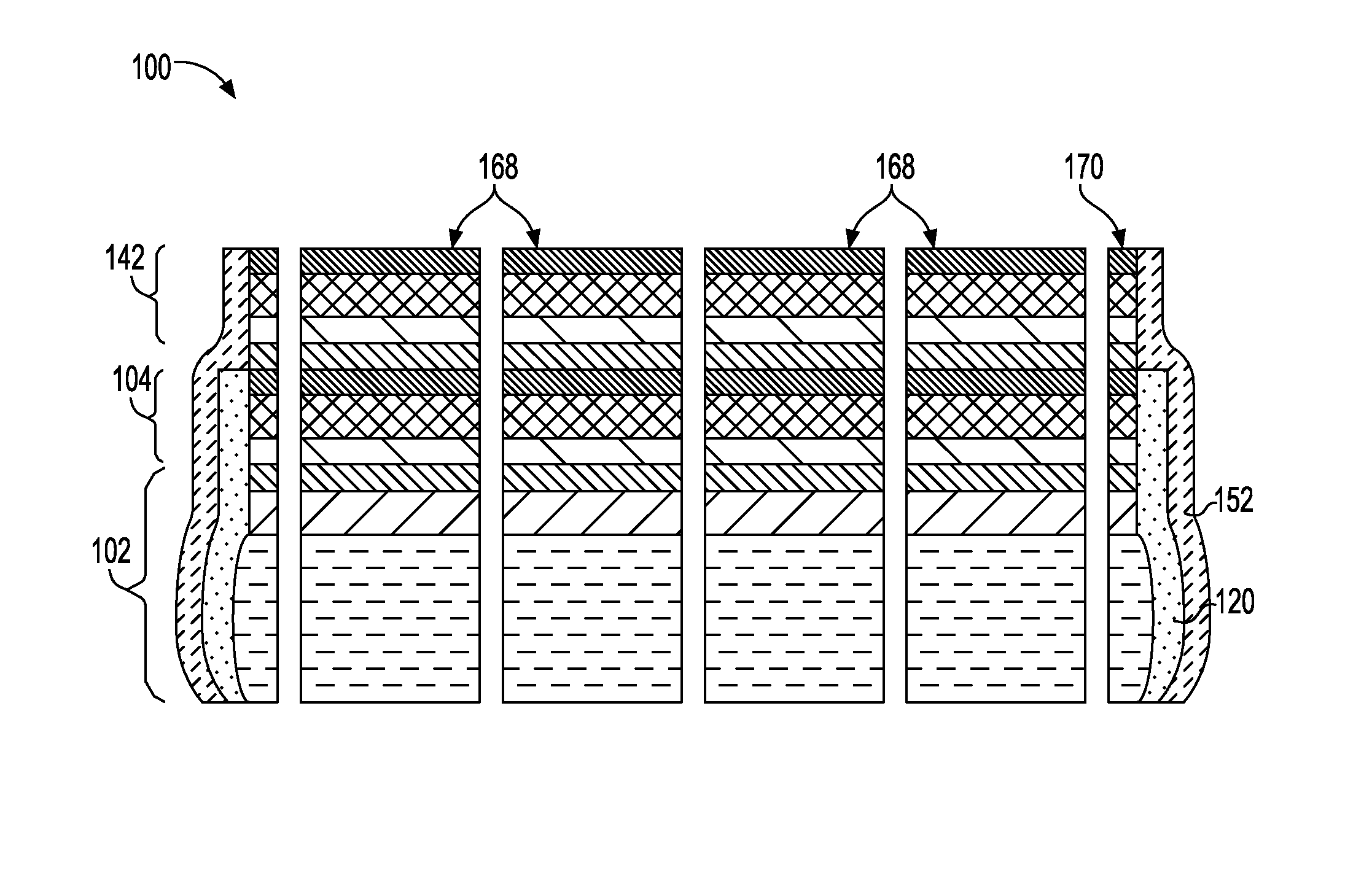
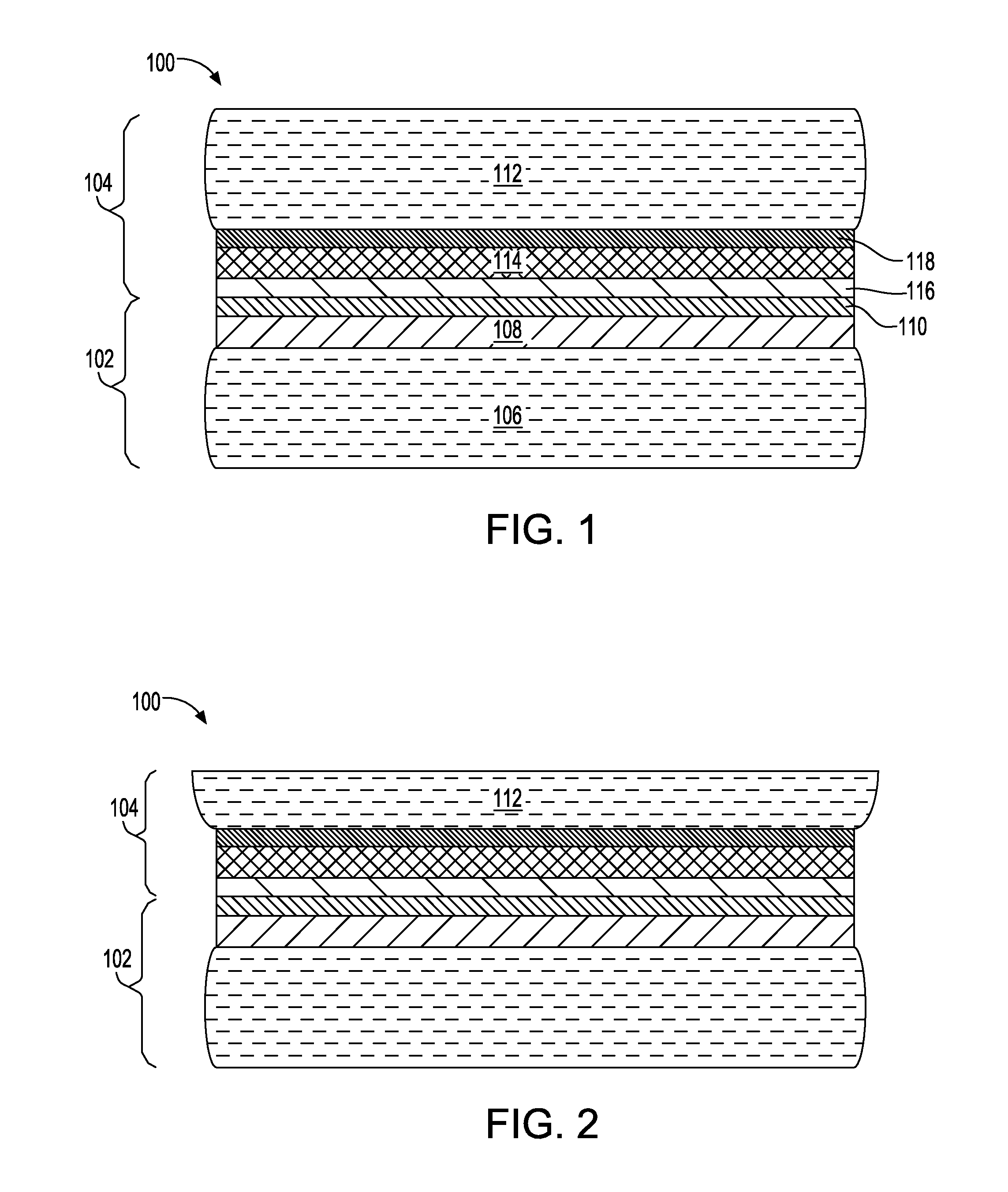
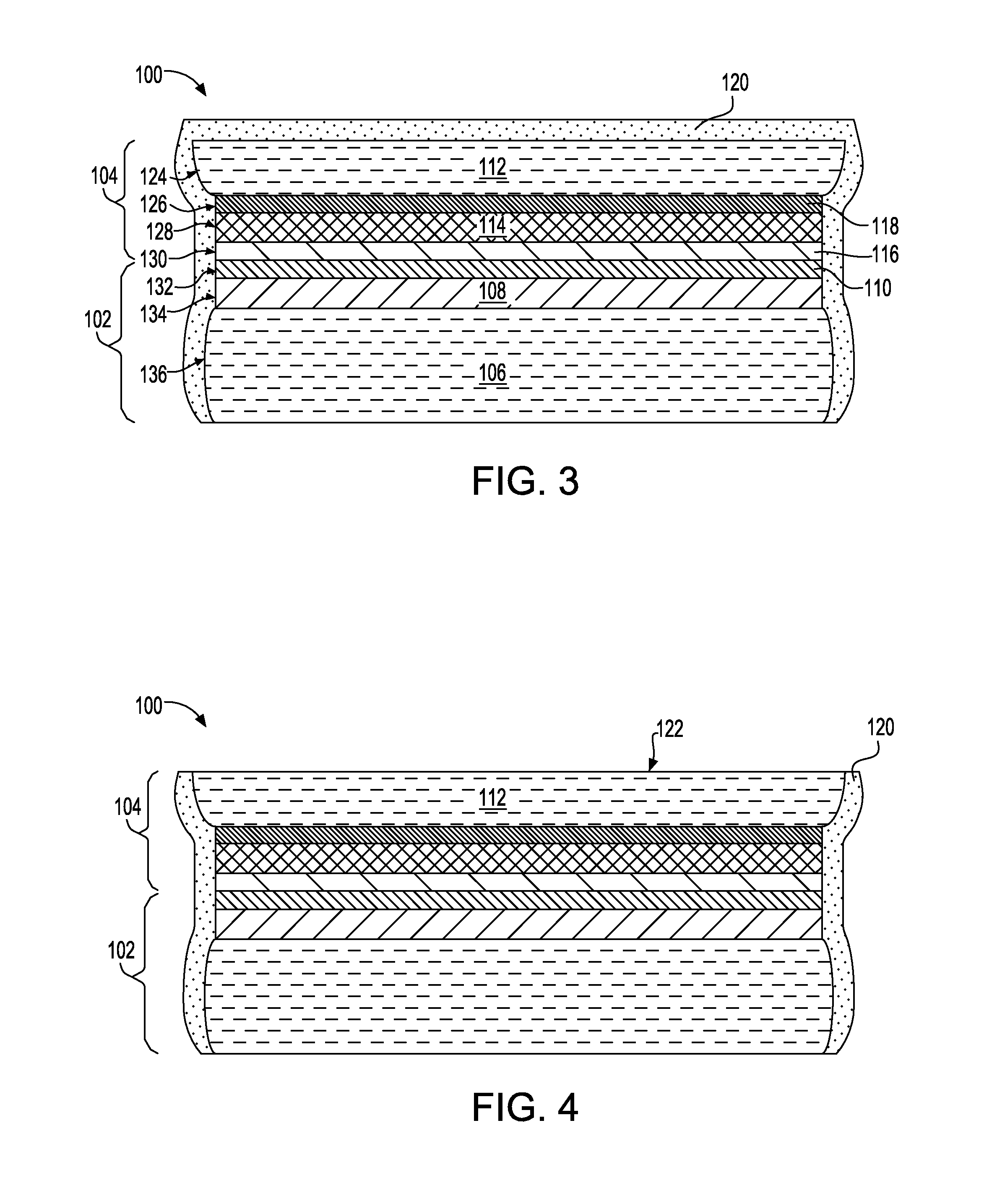
- A method involving the application of protective layers on the edges of semiconductor wafers during thinning processes, using conformal deposition techniques like CVD or ALD, to prevent damage from mechanical and wet etching operations, while maintaining these layers throughout subsequent processing steps to ensure edge protection until the wafers are diced into 3D chip stacks.

Quality Control Standards for Wafer Processing
Quality control standards for wafer processing represent a critical framework that governs the precision and reliability of semiconductor manufacturing operations. These standards encompass comprehensive measurement protocols, inspection methodologies, and acceptance criteria that ensure wafer structural integrity throughout thinning and bonding processes. The establishment of rigorous quality benchmarks has become increasingly vital as device miniaturization demands higher precision tolerances and defect-free processing outcomes.
International standards organizations, including SEMI and JEDEC, have developed specific guidelines for wafer processing quality control. These standards define acceptable parameters for surface roughness, thickness uniformity, bow and warp measurements, and contamination levels. For wafer thinning operations, typical thickness tolerance requirements range from ±2-5 micrometers, while surface roughness specifications often mandate Ra values below 0.5 nanometers to ensure optimal bonding performance.
Statistical process control methodologies form the backbone of modern wafer processing quality systems. Real-time monitoring systems continuously track critical parameters such as grinding force, chemical etch rates, and temperature profiles during thinning operations. Advanced metrology tools, including capacitive thickness gauges and optical interferometry systems, provide sub-micrometer measurement accuracy essential for maintaining process control within specified limits.
Bonding quality standards focus on interface integrity assessment through various characterization techniques. Acoustic microscopy, infrared imaging, and mechanical testing protocols evaluate bond strength, void detection, and delamination resistance. Industry standards typically require bond strengths exceeding 1.5 J/m² for permanent bonding applications, with void area percentages maintained below 1% of the total bonded interface.
Contamination control represents another fundamental aspect of quality standards, particularly for particle and ionic contamination management. Clean room protocols, chemical purity specifications, and handling procedures are strictly regulated to prevent defects that could compromise structural integrity. Surface preparation standards mandate specific cleaning sequences and contamination level verification before critical processing steps.
Traceability and documentation requirements ensure comprehensive quality records throughout the manufacturing process. Digital quality management systems track individual wafer histories, process parameters, and inspection results, enabling rapid identification and correction of quality deviations while maintaining regulatory compliance and customer specifications.
International standards organizations, including SEMI and JEDEC, have developed specific guidelines for wafer processing quality control. These standards define acceptable parameters for surface roughness, thickness uniformity, bow and warp measurements, and contamination levels. For wafer thinning operations, typical thickness tolerance requirements range from ±2-5 micrometers, while surface roughness specifications often mandate Ra values below 0.5 nanometers to ensure optimal bonding performance.
Statistical process control methodologies form the backbone of modern wafer processing quality systems. Real-time monitoring systems continuously track critical parameters such as grinding force, chemical etch rates, and temperature profiles during thinning operations. Advanced metrology tools, including capacitive thickness gauges and optical interferometry systems, provide sub-micrometer measurement accuracy essential for maintaining process control within specified limits.
Bonding quality standards focus on interface integrity assessment through various characterization techniques. Acoustic microscopy, infrared imaging, and mechanical testing protocols evaluate bond strength, void detection, and delamination resistance. Industry standards typically require bond strengths exceeding 1.5 J/m² for permanent bonding applications, with void area percentages maintained below 1% of the total bonded interface.
Contamination control represents another fundamental aspect of quality standards, particularly for particle and ionic contamination management. Clean room protocols, chemical purity specifications, and handling procedures are strictly regulated to prevent defects that could compromise structural integrity. Surface preparation standards mandate specific cleaning sequences and contamination level verification before critical processing steps.
Traceability and documentation requirements ensure comprehensive quality records throughout the manufacturing process. Digital quality management systems track individual wafer histories, process parameters, and inspection results, enabling rapid identification and correction of quality deviations while maintaining regulatory compliance and customer specifications.
Cost-Performance Trade-offs in Wafer Manufacturing
The semiconductor industry faces a fundamental economic challenge when balancing wafer thinning and bonding processes to maintain structural integrity. Traditional wafer thinning approaches, while cost-effective for high-volume production, often compromise mechanical strength and yield rates. The grinding and chemical-mechanical polishing processes required for ultra-thin wafers below 50 micrometers significantly increase manufacturing costs due to higher defect rates and specialized handling requirements.
Bonding technologies present alternative cost structures with varying performance implications. Temporary bonding solutions using thermoplastic adhesives offer moderate costs but introduce thermal budget constraints that may affect device performance. Permanent bonding approaches, such as fusion bonding or anodic bonding, require substantial capital investment in specialized equipment and cleanroom facilities, yet provide superior structural integrity for advanced packaging applications.
The economic impact of yield loss becomes particularly pronounced in advanced nodes where wafer costs exceed $15,000 per unit. Structural failures during thinning operations can result in yield losses of 5-15%, directly affecting manufacturing economics. Conversely, robust bonding processes may increase upfront costs by 20-30% but can reduce overall yield loss to below 2%, creating favorable long-term cost dynamics for high-value applications.
Manufacturing scalability introduces additional cost considerations. Wafer-level bonding processes demonstrate better economies of scale compared to die-level approaches, reducing per-unit costs by approximately 40% in high-volume scenarios. However, the initial tooling and process development investments for wafer-level bonding can exceed $50 million, creating significant barriers for smaller manufacturers.
Process integration complexity further influences cost-performance equations. Sequential thinning and bonding operations require multiple handling steps, each introducing potential contamination and damage risks. Advanced through-silicon via integration adds $200-400 per wafer in processing costs but enables superior electrical performance and thermal management capabilities.
The emergence of heterogeneous integration demands increasingly sophisticated bonding solutions that balance structural requirements with thermal and electrical performance. Hybrid bonding technologies, combining metal and dielectric bonding, represent premium solutions with costs 2-3 times higher than conventional approaches but offer unmatched performance for high-end applications requiring sub-10 micrometer pitch interconnects.
Bonding technologies present alternative cost structures with varying performance implications. Temporary bonding solutions using thermoplastic adhesives offer moderate costs but introduce thermal budget constraints that may affect device performance. Permanent bonding approaches, such as fusion bonding or anodic bonding, require substantial capital investment in specialized equipment and cleanroom facilities, yet provide superior structural integrity for advanced packaging applications.
The economic impact of yield loss becomes particularly pronounced in advanced nodes where wafer costs exceed $15,000 per unit. Structural failures during thinning operations can result in yield losses of 5-15%, directly affecting manufacturing economics. Conversely, robust bonding processes may increase upfront costs by 20-30% but can reduce overall yield loss to below 2%, creating favorable long-term cost dynamics for high-value applications.
Manufacturing scalability introduces additional cost considerations. Wafer-level bonding processes demonstrate better economies of scale compared to die-level approaches, reducing per-unit costs by approximately 40% in high-volume scenarios. However, the initial tooling and process development investments for wafer-level bonding can exceed $50 million, creating significant barriers for smaller manufacturers.
Process integration complexity further influences cost-performance equations. Sequential thinning and bonding operations require multiple handling steps, each introducing potential contamination and damage risks. Advanced through-silicon via integration adds $200-400 per wafer in processing costs but enables superior electrical performance and thermal management capabilities.
The emergence of heterogeneous integration demands increasingly sophisticated bonding solutions that balance structural requirements with thermal and electrical performance. Hybrid bonding technologies, combining metal and dielectric bonding, represent premium solutions with costs 2-3 times higher than conventional approaches but offer unmatched performance for high-end applications requiring sub-10 micrometer pitch interconnects.
Unlock deeper insights with Patsnap Eureka Quick Research — get a full tech report to explore trends and direct your research. Try now!
Generate Your Research Report Instantly with AI Agent
Supercharge your innovation with Patsnap Eureka AI Agent Platform!