

Determining Best Practices for Wafer Thinning Process Control
APR 7, 20269 MIN READ
Generate Your Research Report Instantly with AI Agent
PatSnap Eureka helps you evaluate technical feasibility & market potential.
Wafer Thinning Technology Background and Objectives
Wafer thinning technology has emerged as a critical manufacturing process in the semiconductor industry, driven by the relentless pursuit of miniaturization and enhanced device performance. This process involves the systematic reduction of silicon wafer thickness from the standard 725-775 micrometers to ultra-thin dimensions ranging from 25 to 200 micrometers, depending on specific application requirements.
The evolution of wafer thinning began in the 1990s with the advent of advanced packaging technologies and the need for thinner form factors in consumer electronics. Initially developed for memory devices and power semiconductors, the technology has expanded to encompass a broad spectrum of applications including mobile processors, MEMS devices, image sensors, and advanced 3D packaging solutions.
Modern wafer thinning processes primarily utilize mechanical grinding, chemical mechanical polishing (CMP), and wet etching techniques. The mechanical grinding phase employs diamond-embedded grinding wheels to achieve rapid material removal, while subsequent CMP steps ensure surface planarity and minimize subsurface damage. Advanced process control systems monitor critical parameters including grinding force, wheel speed, feed rate, and coolant flow to maintain consistent results across production batches.
The primary objective of establishing best practices for wafer thinning process control centers on achieving optimal balance between throughput, yield, and quality metrics. Key performance indicators include thickness uniformity across the wafer surface, typically targeting less than 2-micrometer variation, surface roughness below 1 nanometer RMS, and minimal subsurface damage depth to preserve device integrity.
Contemporary challenges in wafer thinning process control encompass managing stress-induced warpage, preventing edge chipping, and maintaining dimensional stability during subsequent processing steps. The increasing adoption of ultra-thin wafers below 50 micrometers thickness has intensified these challenges, requiring sophisticated handling systems and real-time monitoring capabilities.
Strategic objectives for process optimization focus on developing predictive control algorithms that can anticipate and compensate for process variations before they impact product quality. This includes implementing advanced sensor technologies for in-situ thickness measurement, surface quality assessment, and stress monitoring throughout the thinning sequence.
Market Demand for Advanced Wafer Thinning Solutions
The semiconductor industry's relentless pursuit of miniaturization and enhanced performance has created substantial market demand for advanced wafer thinning solutions. As electronic devices become increasingly compact while requiring greater functionality, manufacturers face mounting pressure to produce thinner wafers without compromising structural integrity or electrical performance. This demand is particularly pronounced in mobile device manufacturing, where space constraints drive the need for ultra-thin semiconductor components.
The automotive electronics sector represents another significant growth driver for advanced wafer thinning technologies. Modern vehicles incorporate numerous electronic control units, sensors, and power management systems that require reliable thin wafer solutions capable of withstanding harsh operating environments. The transition toward electric vehicles and autonomous driving systems further amplifies this demand, as these applications require sophisticated semiconductor components with optimized thickness profiles.
Consumer electronics manufacturers consistently seek wafer thinning solutions that can achieve precise thickness uniformity while maintaining high throughput rates. The proliferation of wearable devices, Internet of Things applications, and 5G-enabled products has expanded the addressable market for companies offering advanced process control capabilities. These applications demand wafers with thickness variations measured in nanometers, pushing the boundaries of conventional thinning processes.
The memory and storage device market segment exhibits particularly strong demand for innovative wafer thinning approaches. Three-dimensional NAND flash memory and advanced DRAM technologies require precise thickness control to achieve optimal electrical characteristics and thermal management. Manufacturers in this segment prioritize solutions that can deliver consistent results across large wafer batches while minimizing material waste and processing time.
Emerging applications in artificial intelligence, machine learning accelerators, and high-performance computing create additional market opportunities for advanced wafer thinning solutions. These applications often require specialized thickness profiles and surface quality specifications that challenge traditional processing methods. The growing adoption of chiplet architectures and advanced packaging technologies further drives demand for precise wafer thinning capabilities that can support complex multi-die assemblies.
Market dynamics indicate increasing preference for integrated process control systems that combine real-time monitoring, predictive analytics, and automated adjustment capabilities. Manufacturers seek solutions that can reduce process variability, improve yield rates, and minimize the need for manual intervention during wafer thinning operations.
Current Wafer Thinning Process Control Challenges
Wafer thinning process control faces numerous technical challenges that significantly impact semiconductor manufacturing yield and device performance. The primary challenge lies in achieving uniform thickness distribution across the entire wafer surface while maintaining precise dimensional tolerances. Current grinding and polishing processes often result in thickness variations exceeding acceptable limits, particularly at wafer edges where mechanical stress concentrations occur.
Temperature management during thinning operations presents another critical challenge. Excessive heat generation from grinding wheels and chemical-mechanical polishing can cause thermal stress, leading to wafer warpage and micro-crack formation. The difficulty in maintaining consistent cooling across the wafer surface compounds this issue, especially for larger diameter wafers where thermal gradients become more pronounced.
Surface quality control remains problematic due to the inherent trade-off between material removal rate and surface finish. Aggressive thinning parameters increase productivity but often compromise surface integrity, introducing subsurface damage that affects device electrical characteristics. Conversely, conservative approaches may not meet throughput requirements in high-volume manufacturing environments.
Real-time monitoring and feedback control systems face limitations in current implementations. Existing thickness measurement techniques often lack the spatial resolution and measurement speed required for dynamic process adjustment. The challenge is further complicated by the need to measure thickness through various material layers with different optical and mechanical properties.
Contamination control during wet processing steps poses significant challenges, particularly when transitioning between different chemical solutions. Cross-contamination between process baths can alter etch rates and surface chemistry, leading to unpredictable thinning results. The management of chemical waste and environmental compliance adds complexity to process optimization efforts.
Edge handling and protection mechanisms struggle to prevent chipping and micro-cracking during mechanical processing. The mechanical stress concentration at wafer edges makes them particularly vulnerable to damage, which can propagate inward and affect device areas. Current edge protection methods often interfere with uniform processing or introduce additional contamination risks.
Process repeatability across different equipment sets and manufacturing facilities remains inconsistent. Variations in machine calibration, consumable wear patterns, and environmental conditions contribute to process drift over time. The lack of standardized control methodologies makes it difficult to transfer optimized processes between different manufacturing sites or equipment generations.
Current Wafer Thinning Process Control Methods
01 Real-time monitoring and measurement systems for wafer thickness control
Advanced monitoring systems are employed during wafer thinning processes to measure wafer thickness in real-time. These systems utilize various sensing technologies including optical, capacitive, or ultrasonic methods to provide continuous feedback during grinding or polishing operations. The real-time data enables immediate process adjustments to maintain target thickness specifications and improve uniformity across the wafer surface. This approach significantly reduces the risk of over-thinning and wafer breakage while enhancing overall process yield.- Real-time monitoring and measurement systems for wafer thickness control: Advanced monitoring systems are employed during wafer thinning processes to measure wafer thickness in real-time. These systems utilize various sensing technologies including optical, capacitive, or ultrasonic methods to provide continuous feedback during grinding or polishing operations. The real-time data enables immediate process adjustments to maintain target thickness specifications and improve uniformity across the wafer surface. Such monitoring systems help prevent over-grinding and ensure consistent results across multiple wafers in production.
- Endpoint detection methods for wafer thinning processes: Endpoint detection techniques are critical for determining when the desired wafer thickness has been achieved during thinning operations. These methods employ various detection mechanisms including optical interference, acoustic signals, or electrical resistance measurements to identify when the thinning process should be terminated. Accurate endpoint detection prevents damage to device structures and ensures thickness uniformity. The detection systems can be integrated with automated control systems to stop the thinning process at the precise moment the target thickness is reached.
- Automated feedback control systems for grinding and polishing parameters: Automated control systems adjust key process parameters during wafer thinning based on real-time measurements and feedback. These systems regulate variables such as grinding pressure, rotation speed, slurry flow rate, and processing time to maintain optimal thinning conditions. The feedback loops enable dynamic compensation for variations in wafer properties or equipment conditions. Advanced algorithms process sensor data to make continuous adjustments that improve thickness uniformity and reduce defects while maximizing throughput.
- Multi-stage thinning process control with progressive parameter adjustment: Multi-stage thinning approaches employ different control strategies at various phases of the wafer thinning process. Initial rough grinding stages use aggressive parameters for rapid material removal, while subsequent fine grinding and polishing stages employ gentler conditions for surface quality improvement. Each stage has specific control parameters and monitoring requirements tailored to its objectives. The transition between stages is carefully controlled based on thickness measurements and surface condition assessments to optimize both productivity and final wafer quality.
- Statistical process control and quality management for wafer thinning: Statistical process control methods are applied to monitor and maintain wafer thinning process stability over time. These approaches collect and analyze data from multiple wafers and production lots to identify trends, variations, and potential quality issues. Control charts and statistical metrics help operators detect process drift before it results in out-of-specification wafers. The data-driven approach enables continuous process improvement through identification of optimal parameter ranges and correlation of process variables with final wafer quality metrics such as thickness uniformity and surface roughness.
02 Automated feedback control systems for grinding and polishing parameters
Automated control systems are implemented to dynamically adjust grinding and polishing parameters based on measured wafer characteristics. These systems regulate variables such as grinding pressure, rotation speed, feed rate, and abrasive flow to maintain consistent material removal rates. The feedback loops utilize sensor data to compensate for variations in wafer properties, equipment wear, and environmental conditions. This automation ensures precise thickness control and reduces operator dependency while improving process repeatability.Expand Specific Solutions03 Multi-stage thinning process with progressive thickness reduction
Wafer thinning is performed through multiple sequential stages with progressively finer material removal rates. Initial rough grinding stages remove bulk material quickly, followed by intermediate grinding with reduced aggressiveness, and final polishing stages for surface finishing. Each stage employs different abrasive types, grit sizes, and process parameters optimized for that specific phase. This staged approach balances throughput with surface quality while minimizing stress-induced defects and maintaining dimensional control throughout the thinning process.Expand Specific Solutions04 Wafer handling and fixturing methods to prevent damage during thinning
Specialized wafer handling and fixturing techniques are employed to securely hold thin wafers during processing while preventing mechanical damage. These methods include vacuum chucking systems, temporary bonding to carrier substrates, edge protection mechanisms, and controlled loading/unloading procedures. The fixturing systems are designed to distribute forces evenly across the wafer surface and accommodate the reduced mechanical strength of thinned wafers. Proper handling protocols minimize edge chipping, surface scratching, and wafer warpage throughout the thinning workflow.Expand Specific Solutions05 End-point detection and process termination control
Precise end-point detection methods are utilized to determine when the target wafer thickness has been achieved and to terminate the thinning process accordingly. These techniques may involve direct thickness measurement, monitoring of process parameters such as motor current or acoustic emissions, or detection of interface layers. The end-point control systems prevent over-processing and ensure consistent final thickness across production batches. Integration with automated process control enables immediate cessation of material removal upon reaching the specified thickness target.Expand Specific Solutions
Key Players in Wafer Thinning Equipment Industry
The wafer thinning process control market represents a mature segment within the broader semiconductor manufacturing ecosystem, currently valued at several billion dollars and experiencing steady growth driven by advanced packaging demands and miniaturization trends. The industry is in a consolidation phase with established technology maturity, where leading equipment manufacturers like Applied Materials, ASM International, and Tokyo Seimitsu dominate with proven solutions. Major foundries including Taiwan Semiconductor Manufacturing Company, Samsung Electronics, and GLOBALFOUNDRIES drive demand through high-volume production requirements, while memory manufacturers such as Micron Technology push precision boundaries. The competitive landscape features a clear technology hierarchy, with companies like Hwatsing Technology and specialized equipment providers offering targeted solutions for specific thinning applications, indicating a market where incremental innovation and process optimization have become key differentiators rather than breakthrough technological advances.
Applied Materials, Inc.
Technical Solution: Applied Materials has developed comprehensive wafer thinning process control solutions including advanced grinding and polishing systems with real-time thickness monitoring capabilities. Their approach integrates precision mechanical grinding with chemical mechanical planarization (CMP) technology, utilizing in-situ metrology systems for continuous thickness measurement and surface quality assessment. The company's wafer thinning systems feature automated feedback control mechanisms that adjust grinding parameters based on real-time measurements, ensuring uniform thickness distribution across the wafer surface. Their process control methodology includes advanced algorithms for stress management during thinning operations, preventing wafer warpage and cracking through optimized temperature and pressure control protocols.
Strengths: Industry-leading equipment reliability and comprehensive process integration capabilities. Weaknesses: High capital investment requirements and complex system maintenance procedures.
Taiwan Semiconductor Manufacturing Co., Ltd.
Technical Solution: TSMC has established sophisticated wafer thinning process control methodologies focusing on ultra-thin wafer processing for advanced packaging applications. Their approach emphasizes statistical process control (SPC) with extensive data analytics to monitor grinding wheel condition, wafer thickness uniformity, and surface roughness parameters. TSMC's process control framework incorporates machine learning algorithms to predict optimal grinding parameters and prevent defects before they occur. The company has developed proprietary techniques for handling extremely thin wafers (down to 25 micrometers) while maintaining structural integrity, utilizing specialized chuck systems and environmental controls to minimize stress-induced failures during the thinning process.
Strengths: Advanced process analytics and expertise in ultra-thin wafer handling for cutting-edge applications. Weaknesses: Proprietary solutions may limit flexibility and require specialized training for operators.
Core Innovations in Wafer Thinning Process Control
TSV Wafer Thinning Controlling Method and System
PatentInactiveUS20150099423A1
Innovation
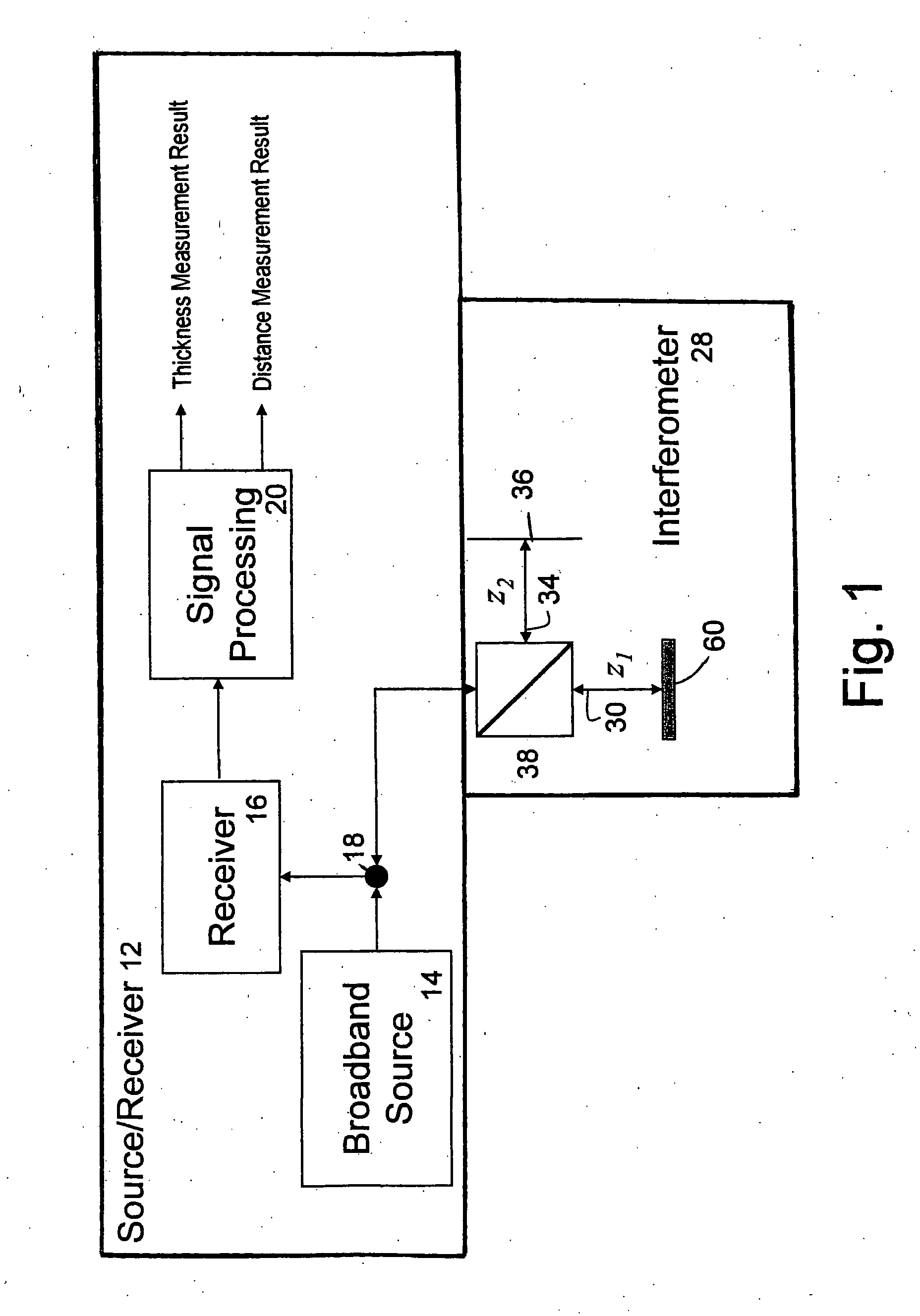
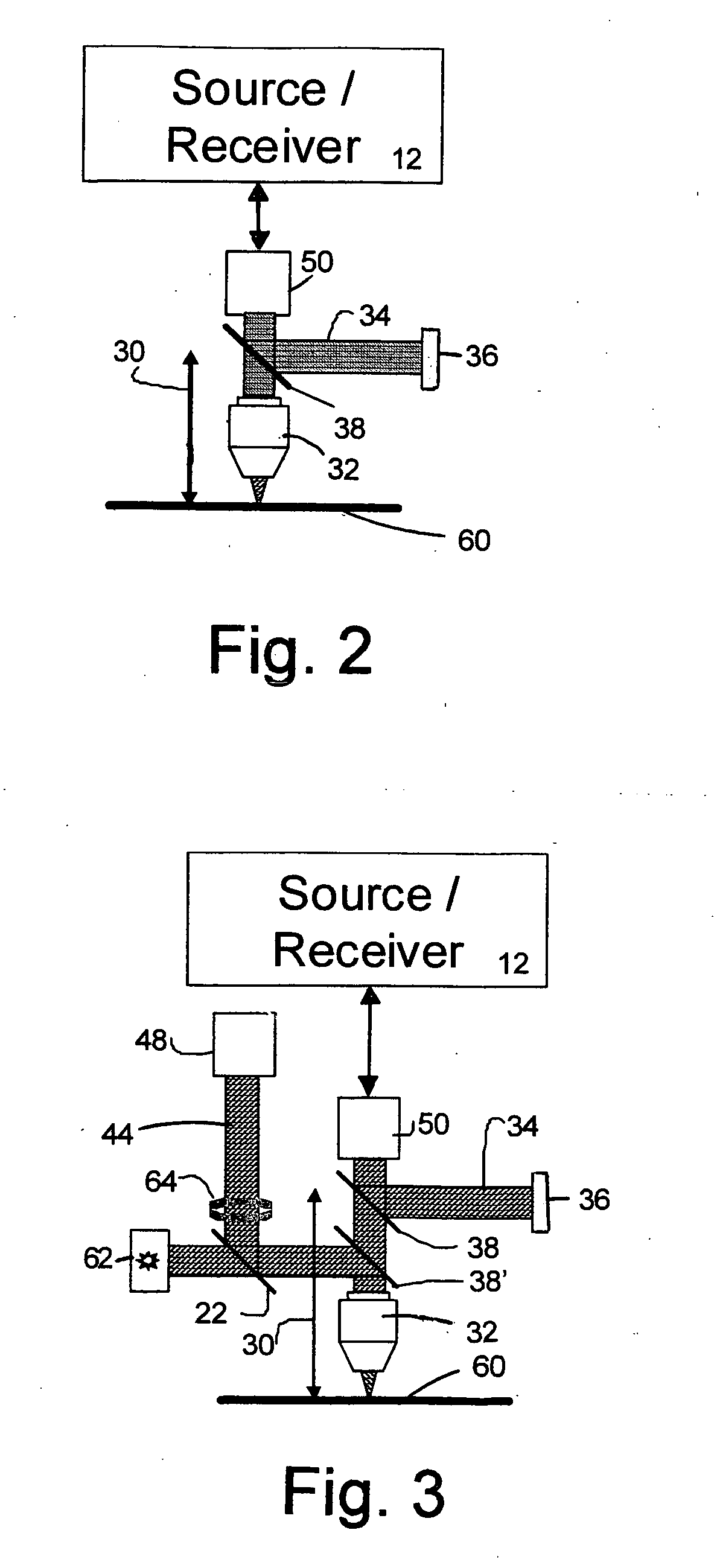
- A TSV wafer thinning controlling method and system utilizing an infrared sensor on a grinding device to measure the distance from the backside of the wafer to the bottom of via-holes through infrared rays emission and reflection, filtering, and signal processing, allowing for precise non-contacting measurement and real-time feedback to terminate the thinning process when the desired distance is reached.


Wafer shape thickness and trench measurement
PatentActiveUS20120257207A1
Innovation
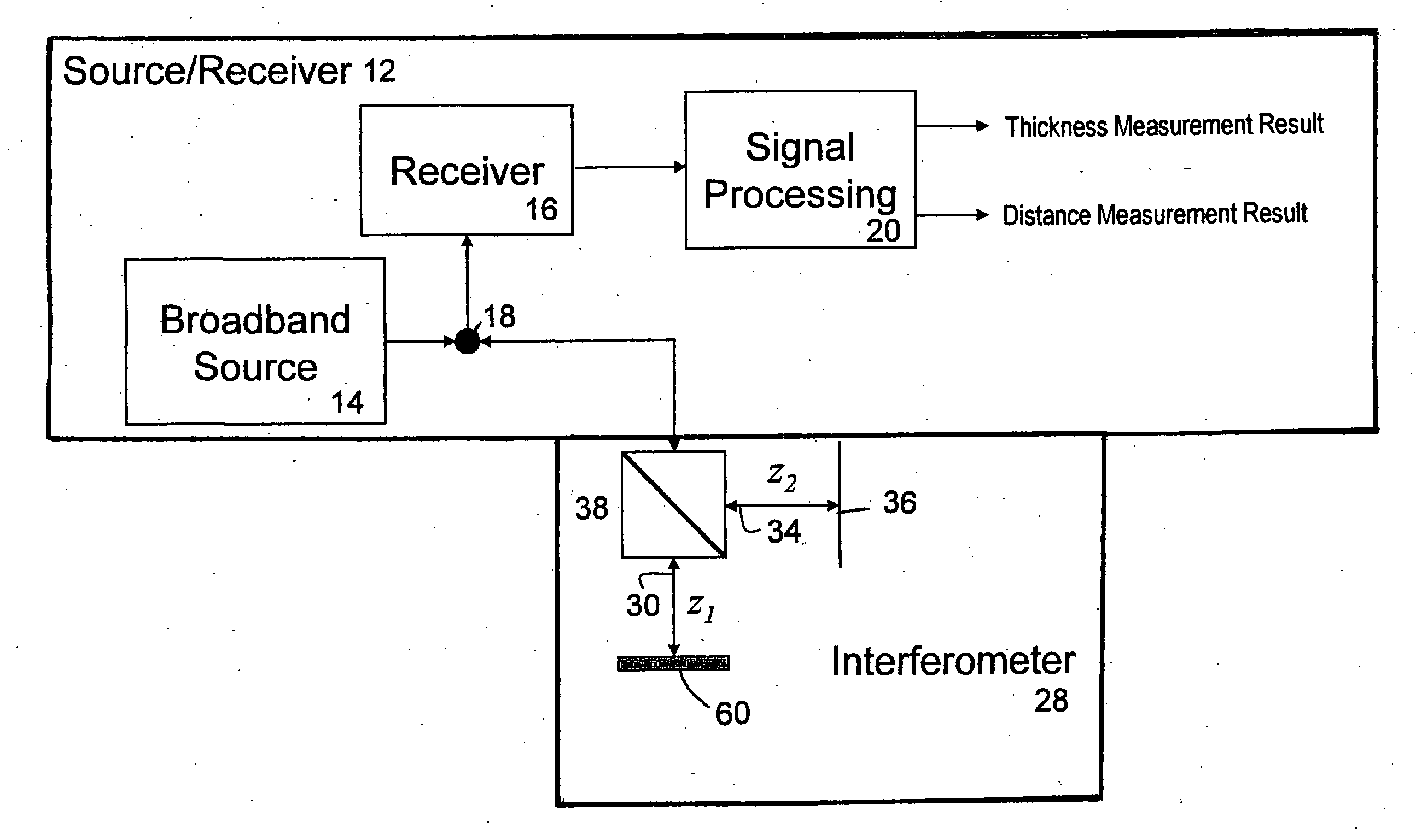
- A device combining a Michelson interferometer with a reflectometer, utilizing a broadband source and signal processing to analyze the reflected spectrum, allowing for simultaneous measurement of wafer thickness, etched feature depth, and three-dimensional shape without axial scanning, including microscopic and macroscopic metrics.

Quality Standards for Semiconductor Wafer Processing
Quality standards for semiconductor wafer processing represent a critical framework that governs the precision and reliability of manufacturing operations across the industry. These standards encompass comprehensive specifications for dimensional tolerances, surface quality metrics, contamination control protocols, and process repeatability requirements. The establishment of rigorous quality benchmarks ensures that wafer thinning operations maintain consistency while meeting the increasingly demanding requirements of advanced semiconductor devices.
International standards organizations, including SEMI and ASTM, have developed detailed specifications that define acceptable parameters for wafer thickness uniformity, total thickness variation (TTV), and bow and warp measurements. These standards typically specify TTV tolerances within ±1-2 micrometers for production wafers, with even tighter requirements for advanced applications. Surface roughness standards mandate Ra values below 0.5 nanometers for critical applications, ensuring optimal performance in subsequent processing steps.
Contamination control standards address both particulate and metallic contamination limits, establishing maximum allowable concentrations measured in parts per billion or particles per square centimeter. These specifications directly impact yield rates and device reliability, making adherence to cleanliness standards essential for commercial viability. Process control standards require statistical process control implementation with capability indices (Cpk) exceeding 1.33 for critical parameters.
Quality assurance protocols mandate comprehensive metrology programs incorporating both inline and offline measurement systems. These programs utilize advanced characterization techniques including laser interferometry, atomic force microscopy, and X-ray fluorescence spectroscopy to verify compliance with established standards. Documentation requirements ensure full traceability throughout the thinning process, enabling rapid identification and correction of deviations.
Emerging quality standards address new challenges posed by ultra-thin wafer processing, including stress-induced defects and handling-related damage. These evolving specifications incorporate predictive quality metrics and real-time monitoring capabilities, reflecting the industry's transition toward more sophisticated process control methodologies that anticipate and prevent quality issues before they impact production outcomes.
Environmental Impact of Wafer Thinning Processes
The environmental impact of wafer thinning processes has become increasingly significant as semiconductor manufacturing scales up globally. Traditional mechanical grinding and chemical etching methods generate substantial waste streams, including silicon particulates, chemical slurries, and contaminated process fluids. These byproducts require specialized treatment and disposal protocols, contributing to the overall environmental footprint of semiconductor fabrication facilities.
Chemical mechanical planarization (CMP) processes, commonly employed in wafer thinning, utilize abrasive slurries containing silica particles and various chemical additives. The disposal of spent slurries presents environmental challenges due to their complex composition and potential toxicity. Additionally, the high water consumption required for cleaning and rinsing operations during thinning processes places considerable strain on local water resources, particularly in regions where semiconductor manufacturing is concentrated.
Energy consumption represents another critical environmental consideration in wafer thinning operations. Plasma etching systems and high-precision grinding equipment require substantial electrical power, contributing to carbon emissions depending on the local energy grid composition. The cooling systems necessary to maintain process temperatures further amplify energy requirements, creating a cascading environmental impact.
Recent regulatory developments have intensified focus on reducing volatile organic compound (VOC) emissions from chemical etching processes. Many traditional thinning chemistries release organic solvents and other volatile compounds that contribute to air quality degradation and potential health hazards for facility workers and surrounding communities.
The semiconductor industry has responded by developing more environmentally sustainable thinning approaches, including dry etching techniques that eliminate liquid waste streams and advanced recycling systems for process chemicals. Water reclamation technologies and closed-loop cooling systems are being implemented to minimize resource consumption. Furthermore, the integration of renewable energy sources in manufacturing facilities is helping to reduce the carbon footprint associated with energy-intensive thinning operations.
Life cycle assessment methodologies are increasingly being applied to evaluate the comprehensive environmental impact of different wafer thinning approaches, enabling manufacturers to make informed decisions about process selection based on sustainability criteria alongside traditional performance and cost considerations.
Unlock deeper insights with PatSnap Eureka Quick Research — get a full tech report to explore trends and direct your research. Try now!
Generate Your Research Report Instantly with AI Agent
Supercharge your innovation with PatSnap Eureka AI Agent Platform!