

Wafer Thinning vs Surface Roughness Considerations Comparison
APR 7, 20269 MIN READ
Generate Your Research Report Instantly with AI Agent
PatSnap Eureka helps you evaluate technical feasibility & market potential.
Wafer Thinning Technology Background and Objectives
Wafer thinning technology has emerged as a critical process in semiconductor manufacturing, driven by the relentless pursuit of miniaturization and enhanced device performance. This technology involves reducing the thickness of silicon wafers from their standard 725-775 micrometers to ultra-thin dimensions, often below 50 micrometers, to meet the demanding requirements of modern electronic applications.
The evolution of wafer thinning can be traced back to the early 2000s when the semiconductor industry began recognizing the need for thinner substrates to enable three-dimensional packaging architectures. Initially developed for memory applications, the technology has expanded across various semiconductor segments, including logic devices, power electronics, and MEMS applications. The progression from mechanical grinding to advanced chemical-mechanical processes represents a significant technological leap in achieving precise thickness control.
The fundamental challenge in wafer thinning lies in balancing thickness reduction with surface quality preservation. As wafers become thinner, they become increasingly susceptible to mechanical stress, warpage, and surface defects. Surface roughness emerges as a critical parameter that directly impacts device performance, yield, and reliability. The relationship between thinning processes and surface roughness is complex, involving multiple interdependent factors including grinding parameters, chemical etching conditions, and post-processing treatments.
Current technological objectives focus on achieving sub-10 micrometer thickness variations across entire wafer surfaces while maintaining surface roughness values below 1 nanometer RMS. Advanced thinning processes aim to eliminate subsurface damage typically introduced during mechanical grinding operations, which can propagate as microcracks and compromise device integrity. The industry seeks to develop integrated process flows that combine precision material removal with real-time surface quality monitoring.
The strategic importance of wafer thinning technology extends beyond traditional semiconductor applications into emerging fields such as flexible electronics, biomedical devices, and advanced packaging solutions. Future objectives include developing temperature-controlled thinning processes, implementing in-situ surface characterization techniques, and establishing predictive models for surface roughness optimization based on process parameters and material properties.
Market Demand for Ultra-Thin Wafer Applications
The semiconductor industry is experiencing unprecedented demand for ultra-thin wafer applications, driven by the relentless pursuit of miniaturization and enhanced performance across multiple technology sectors. This demand surge stems from the fundamental need to reduce device thickness while maintaining or improving electrical performance, thermal management, and mechanical reliability.
Mobile electronics represent the largest market segment driving ultra-thin wafer adoption. Smartphones, tablets, and wearable devices require increasingly compact form factors without compromising functionality. The integration of multiple sensors, processors, and memory components within limited space necessitates wafer thickness reduction to enable three-dimensional packaging architectures and system-in-package solutions.
The automotive electronics sector has emerged as a significant growth driver for ultra-thin wafer technologies. Advanced driver assistance systems, electric vehicle power management, and autonomous driving capabilities demand high-density electronic integration. Ultra-thin wafers enable the development of compact sensor arrays, power management integrated circuits, and high-frequency communication modules essential for next-generation automotive applications.
Memory and storage applications constitute another critical market segment. The transition toward three-dimensional NAND flash memory structures and high-bandwidth memory architectures requires precise wafer thinning capabilities. These applications demand extremely tight thickness uniformity and minimal surface roughness to ensure reliable electrical connections and optimal performance characteristics.
Emerging applications in flexible electronics and Internet of Things devices are creating new market opportunities for ultra-thin wafer technologies. Flexible displays, bendable sensors, and conformable electronic systems require substrates with exceptional thinness while maintaining structural integrity. The growing deployment of IoT sensors across industrial, healthcare, and consumer applications further amplifies the demand for miniaturized semiconductor solutions.
The 5G infrastructure rollout and millimeter-wave communication systems present additional market drivers. High-frequency applications require specialized packaging solutions that minimize signal loss and electromagnetic interference, making ultra-thin wafer processing essential for radio frequency component manufacturing.
Market growth is also fueled by the increasing adoption of advanced packaging technologies such as through-silicon vias, wafer-level chip-scale packaging, and fan-out wafer-level packaging. These technologies rely heavily on precise wafer thinning processes to achieve the required electrical and thermal performance characteristics while maintaining cost-effectiveness in high-volume manufacturing environments.
Current Wafer Thinning Challenges and Surface Quality Issues
Wafer thinning processes face significant challenges in achieving ultra-thin substrates while maintaining acceptable surface quality standards. The semiconductor industry's push toward thinner wafers for advanced packaging applications has intensified the complexity of balancing thickness reduction with surface integrity preservation. Current manufacturing processes struggle to consistently achieve target thicknesses below 50 micrometers without introducing critical surface defects that compromise device performance and yield.
Mechanical grinding remains the primary thinning method, but it inherently generates subsurface damage and micro-cracks that extend several micrometers into the silicon substrate. These defects manifest as increased surface roughness, typically ranging from 0.5 to 2.0 micrometers Ra, which exceeds acceptable limits for many advanced applications. The grinding wheel selection, feed rates, and coolant management directly impact the severity of surface damage, creating a complex optimization challenge for process engineers.
Chemical mechanical polishing (CMP) processes, while effective at reducing surface roughness to nanometer levels, introduce their own set of challenges. The removal rates are significantly slower than mechanical grinding, leading to extended processing times and increased manufacturing costs. Additionally, CMP processes can create surface contamination issues and require precise control of slurry chemistry, pad conditioning, and pressure distribution to maintain uniformity across large wafer surfaces.
Plasma etching and wet chemical etching alternatives offer potential solutions for damage-free thinning but face scalability and uniformity challenges. Plasma processes can achieve excellent surface quality but suffer from edge effects and non-uniform etch rates across the wafer surface. Wet chemical methods provide isotropic etching characteristics but require extensive masking and present environmental and safety concerns due to hazardous chemical usage.
The interaction between thinning-induced stress and surface quality presents another critical challenge. As wafer thickness decreases, mechanical stress concentrations increase dramatically, leading to warpage, bow, and potential fracture during handling. These stress-related deformations directly impact surface flatness and can introduce additional roughness variations across the wafer surface, particularly near the edges where stress concentrations are highest.
Temperature management during thinning processes significantly affects surface quality outcomes. Excessive heat generation during grinding operations can cause thermal stress, leading to crystal lattice damage and increased surface roughness. Inadequate cooling can result in material phase changes and the formation of amorphous layers that degrade electrical properties and create non-uniform surface characteristics.
Quality control and metrology challenges compound these technical difficulties. Traditional surface measurement techniques may not adequately capture the full spectrum of surface defects relevant to device performance. The correlation between measured surface parameters and actual device functionality remains poorly understood, making it difficult to establish appropriate specification limits and process control strategies for next-generation applications.
Existing Wafer Thinning Solutions and Surface Treatments
01 Chemical mechanical polishing (CMP) methods for controlling wafer surface roughness
Chemical mechanical polishing is a key technique used to reduce wafer surface roughness by combining chemical reactions with mechanical abrasion. This process involves the use of polishing slurries containing abrasive particles and chemical agents that react with the wafer surface. The method allows for precise control of surface planarity and roughness at the nanometer scale, which is critical for semiconductor device fabrication. Various parameters such as polishing pressure, pad characteristics, and slurry composition can be optimized to achieve desired surface roughness values.- Chemical mechanical polishing (CMP) methods for controlling wafer surface roughness: Chemical mechanical polishing is a key technique used to reduce wafer surface roughness by combining chemical reactions with mechanical abrasion. This method involves the use of polishing slurries containing abrasive particles and chemical agents that react with the wafer surface. The process parameters such as polishing pressure, rotation speed, and slurry composition can be optimized to achieve desired surface roughness levels. Advanced CMP processes incorporate real-time monitoring and feedback control systems to maintain consistent surface quality across the entire wafer.
- Measurement and characterization techniques for wafer surface roughness: Various measurement techniques are employed to accurately characterize wafer surface roughness, including atomic force microscopy, optical profilometry, and laser scattering methods. These techniques provide quantitative data on surface topography parameters such as average roughness, root mean square roughness, and peak-to-valley height. Advanced measurement systems integrate multiple sensing technologies to provide comprehensive surface analysis. In-line measurement capabilities enable real-time process monitoring and quality control during wafer manufacturing.
- Plasma treatment and etching processes for surface roughness modification: Plasma-based processes are utilized to modify wafer surface roughness through controlled etching or deposition. These processes use ionized gases to selectively remove or add material to the wafer surface, enabling precise control of surface topography. Process parameters such as gas composition, pressure, power, and treatment time can be adjusted to achieve specific roughness characteristics. Plasma treatments can be used for surface smoothing or intentional roughening depending on the application requirements.
- Post-processing cleaning and conditioning methods for roughness control: Post-processing cleaning and conditioning steps are critical for maintaining optimal wafer surface roughness after primary manufacturing processes. These methods include wet chemical cleaning, brush scrubbing, and megasonic cleaning to remove particles and residues that affect surface quality. Specialized cleaning solutions and process sequences are designed to minimize surface damage while effectively removing contaminants. Surface conditioning treatments can also be applied to stabilize the surface and prevent roughness degradation during subsequent processing steps.
- Substrate material selection and preparation for roughness optimization: The selection and preparation of substrate materials play a fundamental role in determining final wafer surface roughness. Different substrate materials exhibit varying inherent roughness characteristics based on their crystalline structure and manufacturing methods. Pre-processing steps such as grinding, lapping, and initial polishing establish the baseline surface quality. Material properties including crystal orientation, doping concentration, and defect density influence the achievable surface roughness. Advanced substrate preparation techniques incorporate multi-stage processing to progressively reduce surface roughness to nanometer-scale levels.
02 Measurement and inspection techniques for wafer surface roughness
Advanced measurement techniques are essential for accurately characterizing wafer surface roughness. These methods include optical inspection systems, atomic force microscopy, and laser scattering techniques that can detect surface irregularities at the nanometer scale. Real-time monitoring systems enable in-situ measurement during processing, allowing for immediate feedback and process adjustments. Statistical analysis of roughness parameters helps establish quality control standards and correlate surface characteristics with device performance.Expand Specific Solutions03 Wafer cleaning and conditioning processes to minimize surface roughness
Pre-processing and post-processing cleaning steps play a crucial role in maintaining low surface roughness. These processes remove contaminants, particles, and residues that can contribute to surface irregularities. Wet cleaning methods using specific chemical solutions, as well as dry cleaning techniques, are employed to prepare wafer surfaces. Conditioning treatments can also modify surface properties to reduce roughness and improve uniformity across the wafer.Expand Specific Solutions04 Substrate material selection and preparation affecting surface roughness
The choice of substrate material and its initial preparation significantly impacts the final surface roughness achievable. Different crystalline orientations, doping levels, and material compositions exhibit varying responses to processing steps. Surface preparation techniques such as grinding, lapping, and initial polishing establish the baseline roughness before subsequent processing. Material properties including hardness, chemical reactivity, and crystal structure influence how the surface responds to polishing and etching operations.Expand Specific Solutions05 Equipment design and process control for achieving target surface roughness
Specialized equipment design features and process control strategies are implemented to consistently achieve target surface roughness specifications. This includes precision control of processing parameters such as temperature, pressure, rotation speed, and chemical flow rates. Equipment components like polishing pads, backing films, and carrier designs are optimized for uniform material removal. Automated control systems monitor multiple parameters simultaneously and make real-time adjustments to maintain process stability and minimize roughness variations across wafers and between batches.Expand Specific Solutions
Key Players in Wafer Processing Equipment Industry
The wafer thinning versus surface roughness considerations comparison represents a mature semiconductor manufacturing challenge within a well-established industry valued at over $500 billion globally. The competitive landscape features established Japanese leaders like DISCO Corp., Tokyo Seimitsu, and Shin-Etsu Handotai dominating precision processing equipment and substrate manufacturing, while companies such as Soitec SA and SUMCO Corp. lead in advanced wafer technologies. Chinese players including SMIC and Ningbo Semiconductor International are rapidly advancing capabilities. Technology maturity varies significantly - while basic thinning processes are well-established, advanced solutions balancing ultra-thin requirements with minimal surface roughness remain challenging. Equipment manufacturers like Veeco Instruments and specialized firms such as Micro Engineering continue innovating to address increasingly stringent specifications for next-generation semiconductor devices requiring sub-micron thickness control.
DISCO Corp.
Technical Solution: DISCO specializes in precision cutting, grinding, and polishing equipment for semiconductor wafer processing. Their wafer thinning solutions utilize advanced grinding wheels and polishing technologies to achieve ultra-thin wafer profiles while maintaining strict surface roughness specifications. The company's DGP (Dicing, Grinding, Polishing) systems integrate multiple processes to optimize the balance between thinning efficiency and surface quality. Their grinding technology can achieve wafer thickness down to 25μm with surface roughness Ra values below 0.5nm through proprietary wheel design and process control algorithms.
Strengths: Industry-leading precision in wafer thinning with excellent surface finish control, comprehensive integrated processing solutions. Weaknesses: High equipment costs and complex process optimization requirements.
Tokyo Seimitsu Co., Ltd.
Technical Solution: Tokyo Seimitsu develops advanced wafer grinding and polishing equipment that addresses the critical balance between wafer thinning and surface roughness control. Their systems employ multi-stage grinding processes with progressively finer abrasives, followed by chemical mechanical polishing (CMP) to achieve target thickness while minimizing surface defects. The company's technology focuses on stress-free grinding techniques that prevent wafer warpage and maintain uniform thickness distribution. Their equipment can process wafers down to 50μm thickness with surface roughness specifications meeting advanced packaging requirements for 3D integration applications.
Strengths: Excellent stress control during thinning processes, proven track record in high-volume manufacturing. Weaknesses: Limited flexibility for extremely thin wafer applications below 50μm, longer processing times compared to some competitors.
Core Innovations in Surface Roughness Control Methods
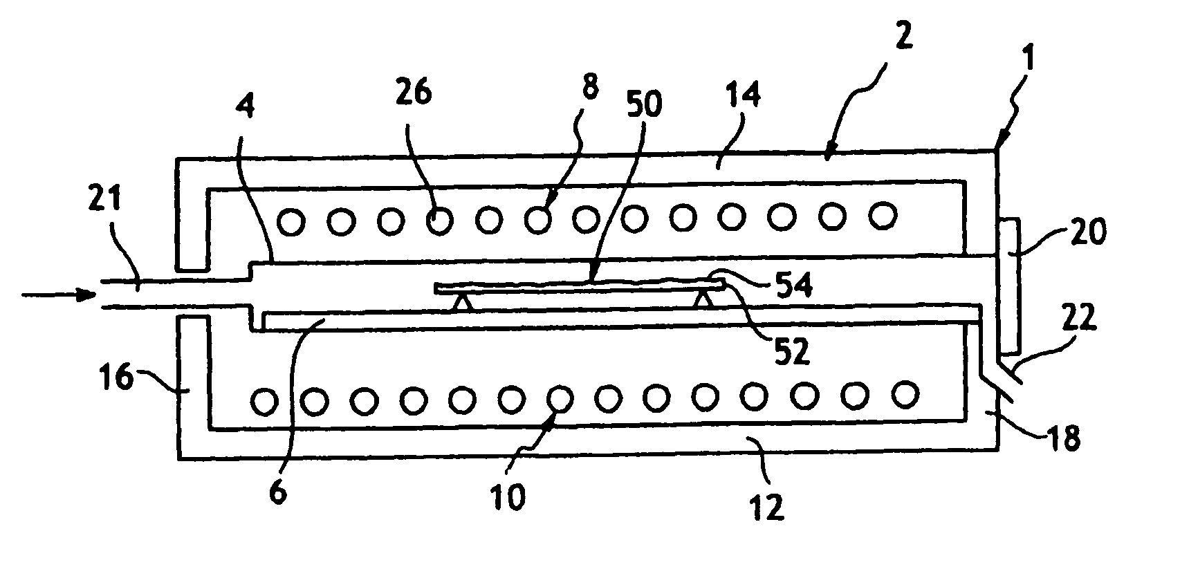
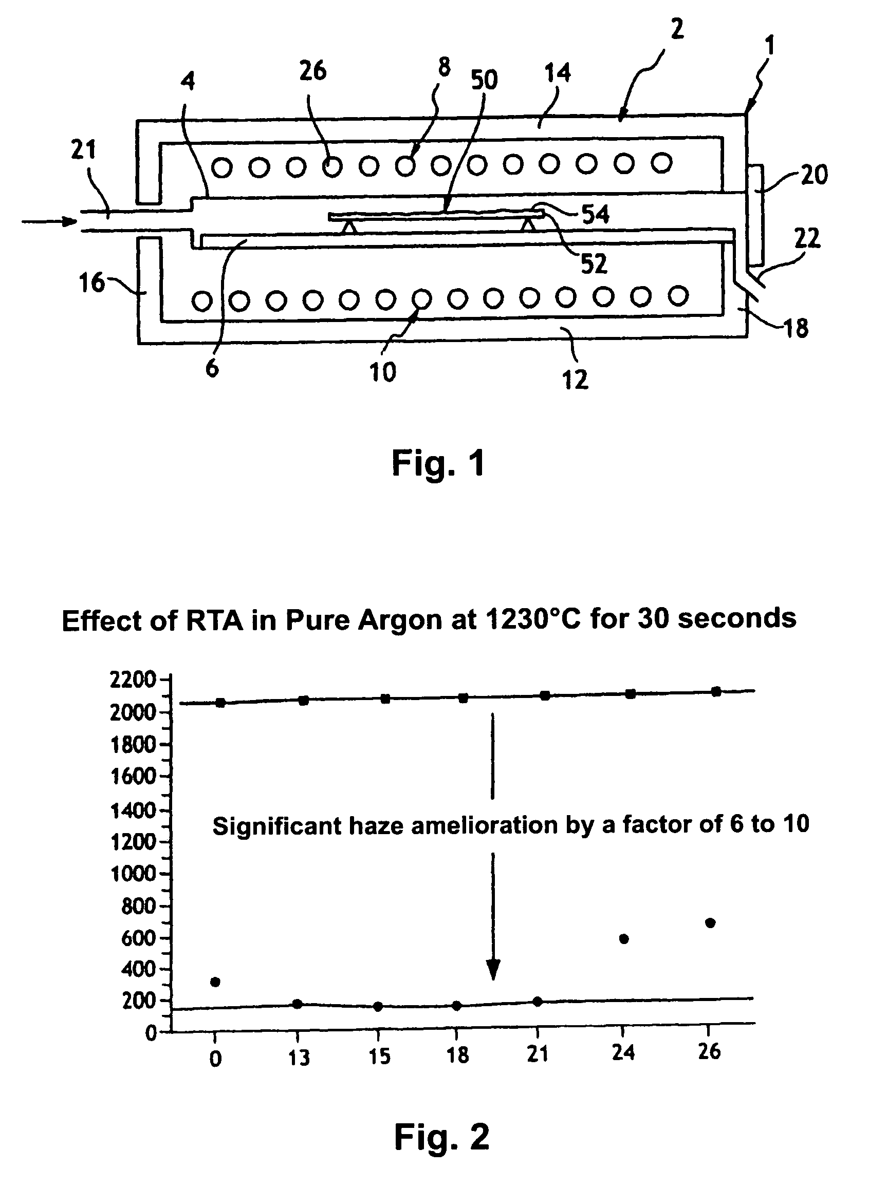
Method of reducing the surface roughness of a semiconductor wafer
PatentInactiveUS7749910B2
Innovation
- A method involving material removal from the wafer surface through polishing or chemical cleaning, followed by rapid thermal annealing in a pure argon atmosphere to reduce roughness, with optional additional sacrificial oxidation and polishing steps, to achieve homogeneous surface smoothing.
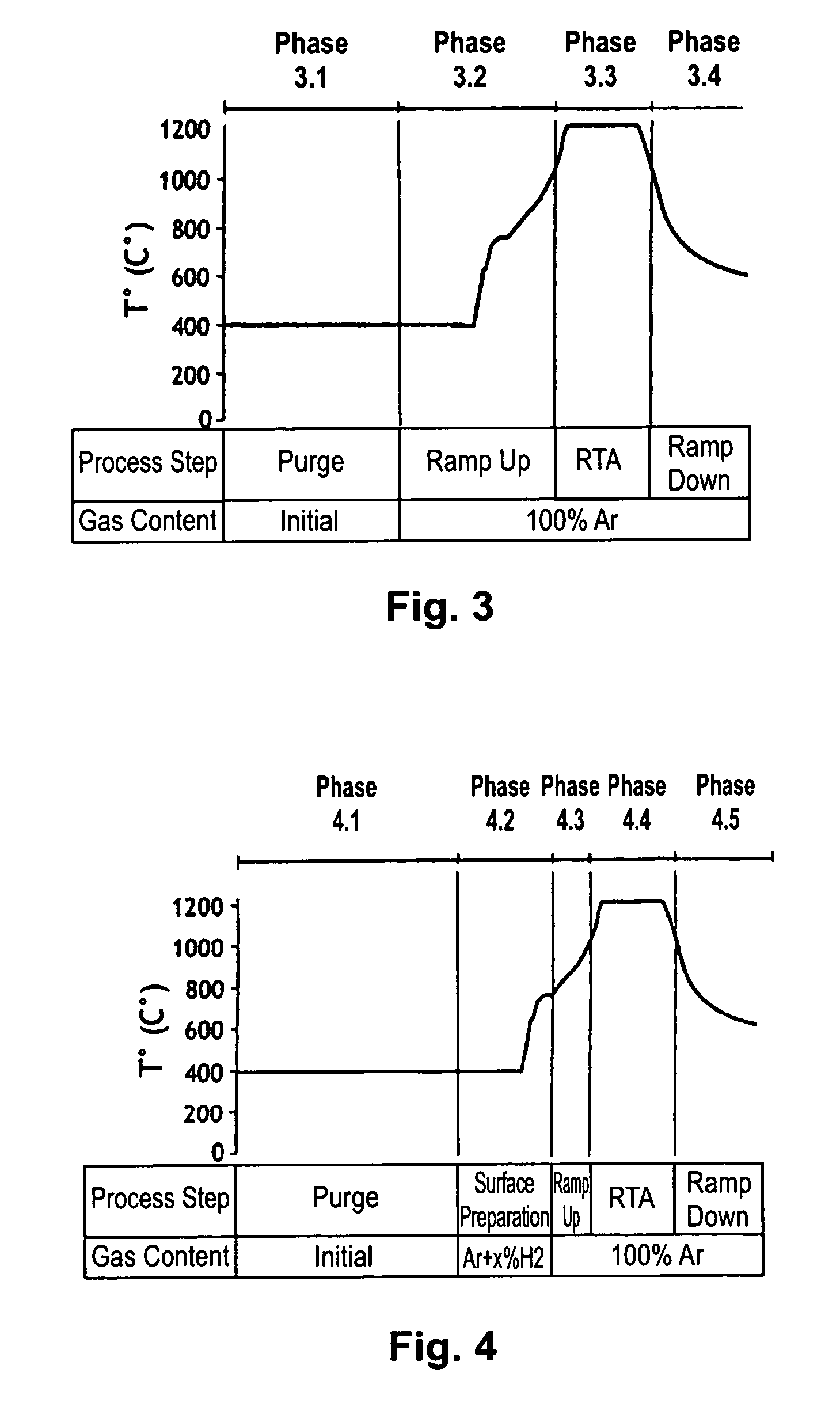

Method for improving the surface roughness of a silicon-on-insulator wafer
PatentInactiveUS20230137992A1
Innovation
- A method involving rapid thermal treatment with controlled gas composition and temperature processes, where the wafer is initially treated in pure argon at 100° C. to 400° C., then switched to a mixed argon and hydrogen atmosphere for heating to 1150° C. to 1300° C., followed by annealing and cooling in pure argon, to achieve a surface roughness of less than 5Å.


Equipment Standards for Semiconductor Manufacturing
The semiconductor manufacturing industry operates under stringent equipment standards that directly impact wafer thinning processes and surface roughness outcomes. International standards organizations, including SEMI (Semiconductor Equipment and Materials International) and ISO (International Organization for Standardization), have established comprehensive guidelines governing equipment specifications, calibration procedures, and performance metrics for wafer processing tools.
Equipment standards for wafer thinning operations encompass multiple critical parameters including grinding wheel specifications, chuck flatness tolerances, and spindle runout limits. SEMI standard M1-0302 defines requirements for wafer handling equipment, specifying maximum allowable surface contamination levels and mechanical stress thresholds. These standards ensure that thinning equipment maintains consistent performance across different manufacturing facilities and process conditions.
Surface roughness measurement equipment must comply with ISO 25178 standards for three-dimensional surface texture analysis. Atomic force microscopes (AFM) and optical profilometers used in semiconductor facilities require regular calibration against certified reference standards to maintain measurement accuracy within nanometer ranges. Equipment qualification protocols mandate that surface analysis tools demonstrate repeatability and reproducibility metrics meeting industry-specified tolerances.
Process control equipment standards play a crucial role in balancing thinning efficiency with surface quality requirements. Real-time monitoring systems must integrate with manufacturing execution systems (MES) according to SEMI E125 standards for equipment data acquisition and control. These standards ensure that feedback loops between surface roughness measurements and thinning parameters operate within defined response times and accuracy specifications.
Environmental control standards significantly influence equipment performance in wafer thinning applications. Clean room classification requirements under ISO 14644 standards dictate air filtration specifications, temperature stability ranges, and vibration isolation criteria. Equipment installations must demonstrate compliance with these environmental standards to achieve consistent surface roughness results across production batches.
Maintenance and qualification standards establish protocols for equipment performance verification and preventive maintenance scheduling. SEMI E10 guidelines for equipment reliability, availability, and maintainability (RAM) provide frameworks for optimizing equipment uptime while maintaining surface quality specifications throughout extended production runs.
Process Optimization for Yield Enhancement
Process optimization for yield enhancement in wafer thinning operations requires a comprehensive understanding of the intricate relationship between thinning parameters and surface roughness outcomes. The primary objective centers on maximizing production yield while maintaining stringent surface quality specifications that meet downstream packaging and assembly requirements.
The optimization framework begins with establishing critical control parameters that directly influence both thinning efficiency and surface integrity. Key variables include grinding wheel specifications, feed rates, spindle speeds, coolant flow dynamics, and backside grinding pressure distribution. Each parameter exhibits complex interdependencies that must be carefully balanced to achieve optimal yield performance without compromising surface roughness targets.
Statistical process control methodologies play a crucial role in yield enhancement strategies. Implementation of Design of Experiments approaches enables systematic evaluation of parameter interactions, identifying optimal operating windows that maximize throughput while minimizing surface defects. Real-time monitoring systems incorporating advanced metrology tools provide continuous feedback loops for dynamic process adjustment and drift correction.
Yield optimization strategies must account for wafer-to-wafer variations in material properties, including crystal orientation effects, dopant concentration gradients, and initial surface conditions. Adaptive process control algorithms can compensate for these variations by adjusting grinding parameters based on real-time surface roughness measurements and thickness uniformity data.
Equipment maintenance protocols significantly impact yield consistency. Grinding wheel conditioning schedules, spindle bearing maintenance, and coolant system optimization directly correlate with process stability and yield performance. Predictive maintenance approaches utilizing vibration analysis and thermal monitoring help prevent unexpected equipment failures that could compromise yield targets.
Quality gate implementations throughout the thinning process enable early detection of yield-limiting conditions. Inline surface roughness measurements, thickness mapping, and defect detection systems provide critical data for process optimization decisions. Statistical yield models incorporating these quality metrics enable proactive process adjustments before yield degradation occurs.
The integration of machine learning algorithms enhances yield optimization capabilities by identifying subtle process signatures that correlate with yield performance. These advanced analytics tools can predict optimal parameter settings for specific wafer characteristics, enabling personalized process recipes that maximize individual wafer yield potential while maintaining overall production efficiency targets.
Unlock deeper insights with PatSnap Eureka Quick Research — get a full tech report to explore trends and direct your research. Try now!
Generate Your Research Report Instantly with AI Agent
Supercharge your innovation with PatSnap Eureka AI Agent Platform!