

Developing Safer Wafer Thinning Techniques for Low-Friction Materials
APR 7, 20269 MIN READ
Generate Your Research Report Instantly with AI Agent
PatSnap Eureka helps you evaluate technical feasibility & market potential.
Wafer Thinning Technology Background and Objectives
Wafer thinning technology has emerged as a critical manufacturing process in the semiconductor industry, driven by the relentless pursuit of miniaturization and enhanced device performance. This technology involves the systematic reduction of silicon wafer thickness from standard dimensions of 725-775 micrometers to ultra-thin profiles ranging from 20 to 100 micrometers, enabling the production of compact electronic devices with improved thermal and electrical characteristics.
The evolution of wafer thinning has been closely intertwined with the advancement of semiconductor packaging technologies, particularly in applications requiring three-dimensional integration, mobile devices, and high-frequency components. Traditional mechanical grinding and chemical-mechanical polishing methods have dominated the field for decades, establishing the foundation for current manufacturing capabilities.
However, the introduction of low-friction materials in semiconductor applications has created unprecedented challenges in conventional thinning processes. These materials, characterized by reduced surface adhesion and altered mechanical properties, exhibit unpredictable behavior during standard thinning operations, leading to increased defect rates, substrate damage, and compromised yield performance.
The primary objective of developing safer wafer thinning techniques for low-friction materials centers on establishing robust processing methodologies that maintain dimensional accuracy while minimizing substrate stress and surface defects. This involves creating adaptive process parameters that can accommodate the unique characteristics of low-friction surfaces without compromising throughput or quality standards.
Key technical goals include achieving uniform thickness distribution across the entire wafer surface, maintaining surface roughness within acceptable limits for subsequent processing steps, and eliminating edge chipping or micro-crack formation that commonly occurs with conventional approaches. Additionally, the development aims to establish predictable process windows that ensure consistent results across different low-friction material compositions.
The strategic importance of this technology extends beyond immediate manufacturing improvements, as it enables the integration of advanced materials in next-generation semiconductor devices. Success in this area will facilitate the adoption of novel substrate materials that offer superior performance characteristics but were previously incompatible with existing manufacturing processes, ultimately expanding the technological possibilities for future electronic systems.
Market Demand for Advanced Wafer Thinning Solutions
The semiconductor industry's relentless pursuit of miniaturization and enhanced performance has created substantial market demand for advanced wafer thinning solutions, particularly for low-friction materials that present unique processing challenges. As electronic devices continue to shrink while requiring greater functionality, manufacturers face increasing pressure to develop thinner wafers without compromising structural integrity or yield rates.
The proliferation of mobile devices, wearable technology, and Internet of Things applications has intensified the need for ultra-thin semiconductor components. These applications demand wafers with thicknesses often below 50 micrometers, pushing conventional thinning techniques to their operational limits. Low-friction materials, including advanced silicon variants and compound semiconductors, exhibit reduced surface adhesion properties that complicate traditional mechanical and chemical thinning processes.
Market drivers extend beyond consumer electronics into high-performance computing, automotive semiconductors, and aerospace applications. The automotive sector's transition toward electric vehicles and autonomous driving systems requires robust yet miniaturized semiconductor solutions capable of withstanding harsh operating environments. These applications necessitate precise thickness control and minimal surface damage during the thinning process.
Current market pain points center around yield loss and quality degradation during wafer thinning operations. Manufacturers report significant challenges with low-friction materials that exhibit poor adhesion to carrier substrates, leading to wafer breakage, non-uniform thickness distribution, and surface contamination. These issues translate directly into increased production costs and reduced manufacturing efficiency.
The demand for safer thinning techniques has intensified as wafer sizes increase and material compositions become more diverse. Advanced packaging technologies, including through-silicon vias and three-dimensional integration schemes, require precise thickness uniformity across large wafer areas. Traditional grinding and chemical etching methods often prove inadequate for achieving the required specifications while maintaining acceptable yield rates.
Emerging applications in flexible electronics and biomedical devices further expand market requirements for specialized thinning solutions. These sectors demand ultra-thin substrates with exceptional surface quality and minimal residual stress, characteristics that conventional thinning methods struggle to deliver consistently for low-friction materials.
The market opportunity encompasses both equipment manufacturers and process technology developers, with particular emphasis on solutions that can handle diverse material properties while maintaining high throughput and yield performance.
Current Challenges in Low-Friction Material Processing
Low-friction materials present unique processing challenges that significantly complicate traditional wafer thinning operations. These materials, characterized by their reduced surface adhesion and enhanced slipperiness, create fundamental difficulties in maintaining secure substrate positioning during mechanical and chemical processing steps. The inherent properties that make these materials valuable for their intended applications simultaneously introduce substantial risks during manufacturing processes.
Mechanical handling represents one of the most critical challenge areas. Conventional vacuum chucking systems often fail to provide adequate holding force on low-friction surfaces, leading to wafer slippage during grinding and polishing operations. This instability not only compromises dimensional accuracy but also creates significant safety hazards as loose wafers can cause equipment damage and pose injury risks to operators. The reduced coefficient of friction between the wafer and handling equipment necessitates entirely new approaches to substrate fixation.
Chemical processing compatibility issues further compound the complexity. Many low-friction materials exhibit poor adhesion to standard protective films and temporary bonding materials used in conventional thinning processes. This incompatibility results in delamination during wet etching or chemical mechanical planarization steps, potentially causing catastrophic process failures and material loss. The chemical inertness that defines these materials often extends to reduced reactivity with standard processing chemicals.
Thermal management during processing presents additional complications. Low-friction materials frequently possess unique thermal expansion coefficients and heat dissipation characteristics that differ significantly from conventional semiconductor substrates. These thermal properties can lead to warpage, stress concentration, and non-uniform processing results during temperature-sensitive thinning operations. The thermal mismatch between low-friction substrates and standard processing equipment creates potential for mechanical failure.
Quality control and metrology challenges emerge from the difficulty in establishing reliable measurement protocols for these materials. Standard surface analysis techniques may not provide accurate readings on low-friction surfaces, complicating thickness monitoring and defect detection. The smooth, non-adherent nature of these materials can interfere with conventional inspection methods, potentially allowing defective products to proceed through manufacturing processes undetected.
Contamination control represents another significant hurdle, as the low-friction properties can affect particle adhesion and removal during cleaning processes. Standard cleaning protocols may prove inadequate, while more aggressive cleaning methods risk damaging the delicate surface properties that define these materials' functionality.
Existing Safe Thinning Methods for Fragile Materials
01 Protective layer application during wafer thinning
Applying protective layers or coatings on wafer surfaces before thinning processes helps prevent damage and cracking. These protective layers can include polymer films, resin materials, or temporary bonding materials that shield the active surface during grinding or polishing operations. The protective layer is removed after thinning is complete, ensuring the integrity of the device structures.- Protective layer application during wafer thinning: Applying protective layers or coatings on wafer surfaces before thinning processes helps prevent damage and cracking. These protective layers can include polymer films, resin materials, or temporary bonding materials that shield the active surface during grinding or polishing operations. The protective layer is removed after thinning is completed, ensuring the wafer integrity is maintained throughout the process.
- Stress management and crack prevention techniques: Managing internal stress during wafer thinning is critical for preventing wafer breakage and cracking. Techniques include controlled grinding rates, optimized pressure distribution, and stress-relief processes such as annealing or plasma treatment. Multi-step thinning approaches with gradually decreasing removal rates help minimize stress accumulation and improve wafer strength after thinning.
- Support substrate and carrier wafer methods: Using support substrates or carrier wafers during thinning operations provides mechanical stability and prevents wafer warping or breakage. The thin wafer is temporarily bonded to a thicker carrier using adhesives or bonding materials, allowing safe handling during processing. After thinning, the carrier is debonded using thermal, chemical, or mechanical methods without damaging the thinned wafer.
- Edge protection and chamfering techniques: Protecting wafer edges during thinning prevents edge chipping and crack initiation. Edge chamfering or rounding processes remove sharp corners that are prone to damage. Edge protection methods include applying protective tapes, using specialized edge grinding tools, or implementing controlled edge removal processes that create smooth, rounded edges less susceptible to mechanical failure.
- Process monitoring and quality control systems: Real-time monitoring systems track critical parameters during wafer thinning to ensure safety and quality. These systems measure thickness uniformity, detect cracks or defects, monitor grinding forces and temperatures, and provide feedback for process adjustment. Automated inspection systems using optical or acoustic methods identify potential safety issues before catastrophic failure occurs, improving yield and reducing wafer loss.
02 Controlled grinding and polishing parameters
Implementing precise control of grinding and polishing parameters such as pressure, speed, and temperature ensures safe wafer thinning. Monitoring and adjusting these parameters in real-time prevents excessive stress, thermal damage, and maintains uniform thickness across the wafer. Advanced feedback systems and sensors enable optimal process control.Expand Specific Solutions03 Support substrate and temporary bonding techniques
Using support substrates or temporary bonding methods provides mechanical stability during thinning operations. The wafer is bonded to a carrier substrate that provides structural support, preventing breakage during handling and processing. Debonding techniques allow safe separation after thinning without damaging the thinned wafer.Expand Specific Solutions04 Stress relief and damage detection methods
Incorporating stress relief processes and damage detection systems enhances safety in wafer thinning. Techniques include controlled cooling, annealing steps, and inspection methods such as optical or acoustic scanning to identify cracks or defects. Early detection allows for process adjustments before catastrophic failure occurs.Expand Specific Solutions05 Chemical mechanical planarization safety measures
Chemical mechanical planarization processes incorporate safety measures including controlled chemical composition, pH monitoring, and waste handling protocols. Proper selection of slurry materials and process conditions minimizes chemical hazards while achieving desired thinning results. Equipment design includes containment systems and automated chemical delivery to reduce operator exposure.Expand Specific Solutions
Major Players in Wafer Processing Equipment Industry
The wafer thinning technology sector for low-friction materials represents a mature yet rapidly evolving market driven by increasing demand for thinner, more efficient semiconductor devices. The industry is experiencing significant growth, particularly in automotive, 5G, and power electronics applications, with market expansion fueled by companies like Applied Materials and Tokyo Seimitsu providing advanced manufacturing equipment. Technology maturity varies across segments, with established players such as SMIC, Micron Technology, and GLOBALFOUNDRIES demonstrating proven capabilities in conventional thinning processes, while specialized firms like SILTECTRA and Soitec are pioneering innovative approaches including Smart Cut technology for engineered substrates. Research institutions like IMEC, Fraunhofer-Gesellschaft, and CEA are advancing next-generation techniques, particularly for challenging materials like silicon carbide (Wolfspeed) and gallium nitride compounds. The competitive landscape shows strong collaboration between equipment manufacturers, foundries, and material suppliers, with companies like Infineon, Texas Instruments, and Shin-Etsu Handotai driving adoption of safer, more precise thinning methodologies to meet stringent quality requirements for advanced semiconductor applications.
SILTECTRA GmbH
Technical Solution: SILTECTRA has pioneered the Cold Split technology for wafer thinning, which uses room-temperature ion implantation followed by mechanical splitting to create ultra-thin layers. This innovative approach is particularly suitable for low-friction materials as it eliminates the thermal stress and mechanical grinding forces that typically cause damage. The process involves implanting hydrogen or helium ions at specific depths to create a weakened layer, then applying controlled mechanical force to split the wafer along this predetermined plane. This technique can achieve thickness uniformity of ±2% across 300mm wafers while maintaining crystal quality. The cold processing nature makes it ideal for temperature-sensitive and mechanically fragile materials, reducing the risk of micro-cracks and surface defects that are common with traditional grinding methods.
Strengths: Minimal thermal stress, excellent thickness uniformity, reduced material waste. Weaknesses: Limited to specific material types, relatively new technology with scaling challenges.
Micron Technology, Inc.
Technical Solution: Micron Technology has developed specialized wafer thinning processes for memory device manufacturing, focusing on ultra-thin die applications down to 15 micrometers thickness. Their approach combines mechanical grinding with plasma etching techniques to achieve precise thickness control while minimizing stress-induced defects. The company utilizes advanced carrier wafer systems and temporary bonding materials specifically designed for low-friction substrates to prevent slippage during processing. Their multi-stage thinning process includes coarse grinding, fine grinding, and plasma back-etch steps, each optimized for different material properties. Micron's proprietary stress relief techniques include controlled temperature cycling and chemical treatments that reduce residual stress in thinned wafers. The process is particularly effective for compound semiconductors and other specialty materials used in high-performance memory applications.
Strengths: Proven high-volume manufacturing capability, excellent yield rates, comprehensive quality control. Weaknesses: Process optimization required for each new material type, limited flexibility for research applications.
Core Patents in Low-Friction Wafer Handling
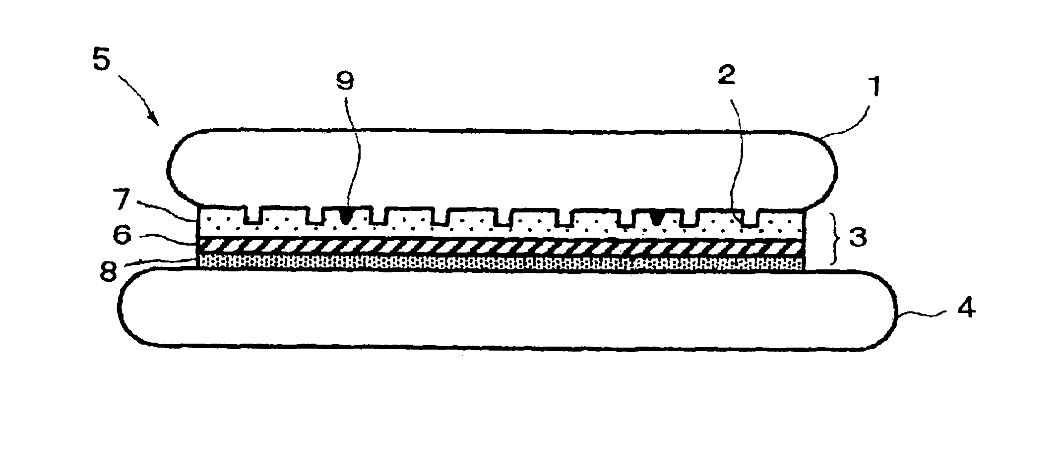
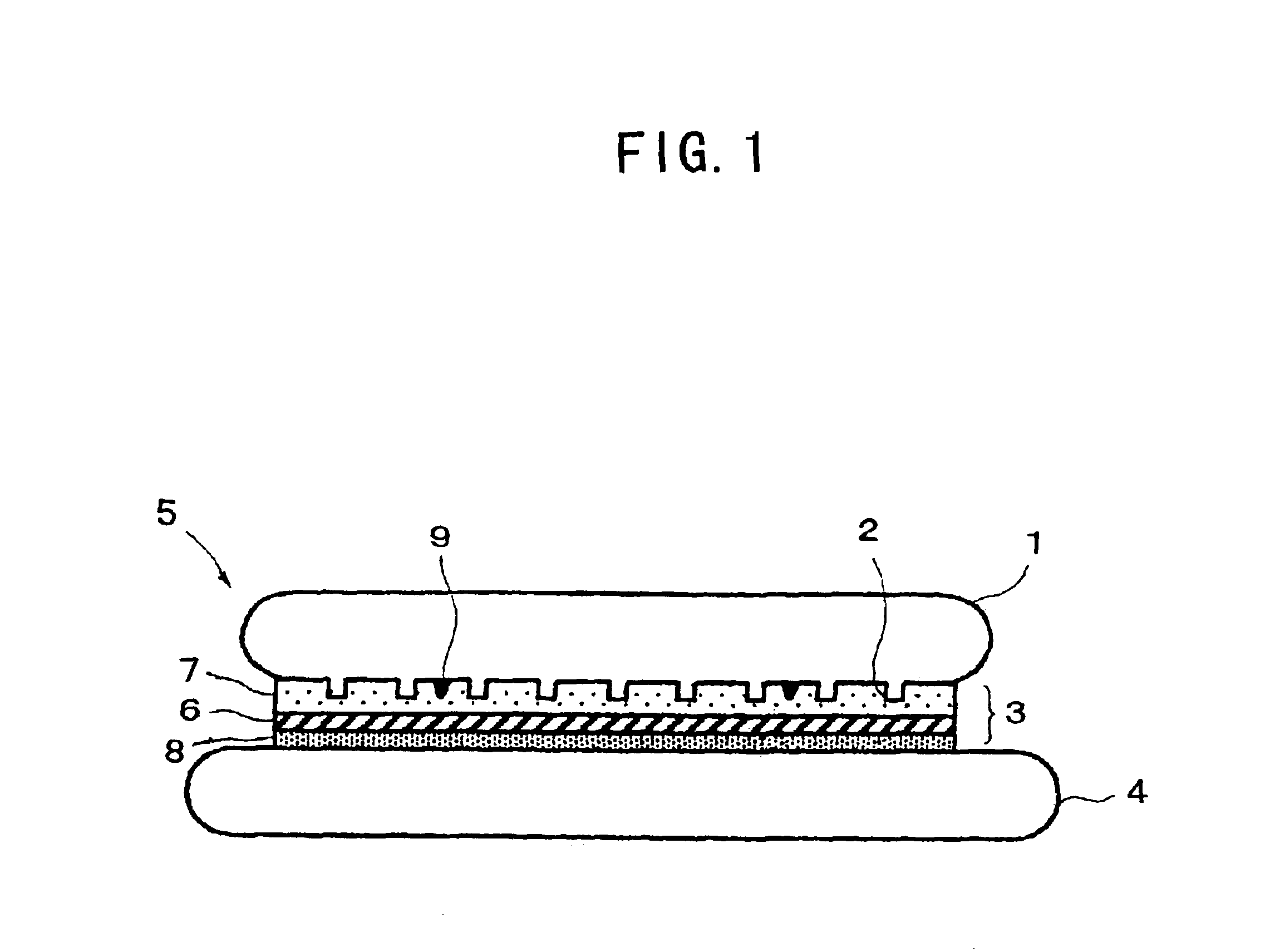
Protective wafer grooving structure for wafer thinning and methods of using the same
PatentPendingUS20240363613A1
Innovation
- A protective wafer grooving structure is implemented, involving the formation of an inter-wafer moat trench and a protective material layer to shield the low-k dielectric materials, along with blade-trimming and additional thinning processes to prevent mechanical and chemical damage.


Semiconductor wafer thinning method, and thin semiconductor wafer
PatentInactiveUS6930023B2
Innovation
- A method involving adhering the semiconductor wafer to a support via an adhesive layer, specifically a thermal release double-sided adhesive sheet, and grinding the back surface to achieve thinner wafers without breakage, allowing for easy release and minimizing stress through matching thermal expansion coefficients and using a larger adhesive surface for secure adhesion.

Environmental Safety Standards for Semiconductor Processing
The semiconductor industry operates under increasingly stringent environmental safety standards that directly impact wafer thinning processes, particularly when handling low-friction materials. These standards encompass air quality regulations, chemical waste management protocols, and worker exposure limits that collectively shape the operational framework for advanced semiconductor manufacturing facilities.
Current environmental regulations mandate strict control of volatile organic compounds (VOCs) and hazardous air pollutants during wafer processing operations. The Environmental Protection Agency's semiconductor manufacturing point source category establishes specific discharge limitations for process wastewater, while OSHA standards define permissible exposure limits for chemicals commonly used in thinning operations such as hydrofluoric acid, sulfuric acid, and various organic solvents.
International standards including ISO 14001 environmental management systems and SEMI safety guidelines provide comprehensive frameworks for environmental compliance in semiconductor facilities. These standards require continuous monitoring of emissions, implementation of best available control technologies, and regular environmental impact assessments. The SEMI S2 safety guideline specifically addresses environmental health and safety requirements for semiconductor manufacturing equipment, establishing baseline requirements for ventilation systems, emergency response procedures, and chemical handling protocols.
Wafer thinning operations involving low-friction materials present unique environmental challenges due to the specialized chemicals and processes required. The reduced adhesion properties of these materials often necessitate modified etching solutions and alternative mechanical processing techniques, which may introduce novel environmental considerations not fully addressed by existing standards. Facilities must implement enhanced containment systems and develop specialized waste treatment protocols to manage the byproducts of these advanced processes.
Emerging regulatory trends indicate a shift toward more comprehensive lifecycle assessments and stricter limits on perfluorinated compounds and other persistent pollutants. The European Union's REACH regulation and similar international frameworks are expanding to cover previously unregulated substances used in semiconductor processing, requiring manufacturers to demonstrate environmental safety through extensive testing and documentation.
Compliance monitoring technologies have evolved to include real-time emissions tracking, automated waste characterization systems, and predictive modeling tools that help facilities maintain regulatory compliance while optimizing process efficiency. These systems enable proactive identification of potential environmental issues and facilitate rapid response to regulatory changes or process deviations.
Quality Control Framework for Ultra-Thin Wafer Production
Establishing a comprehensive quality control framework for ultra-thin wafer production requires implementing multi-layered inspection protocols that address the unique challenges posed by low-friction materials during thinning processes. The framework must integrate real-time monitoring systems with post-process validation techniques to ensure consistent wafer quality while minimizing handling-induced defects.
The foundation of effective quality control lies in implementing in-situ thickness measurement systems that provide continuous feedback during the thinning process. Advanced optical interferometry and capacitive sensing technologies enable precise thickness monitoring without physical contact, reducing the risk of surface damage on delicate low-friction materials. These systems must be calibrated to account for material-specific optical properties and surface characteristics that may vary across different substrate types.
Critical control points throughout the production workflow require standardized inspection procedures that encompass surface roughness analysis, stress distribution mapping, and defect detection protocols. Automated optical inspection systems equipped with high-resolution imaging capabilities can identify micro-cracks, surface irregularities, and contamination that may compromise wafer integrity. The inspection parameters must be tailored to accommodate the reduced mechanical stability of ultra-thin substrates.
Statistical process control methodologies play a crucial role in maintaining production consistency by establishing control limits based on historical performance data and material-specific tolerances. Implementation of Six Sigma principles helps identify process variations that could lead to quality degradation, enabling proactive adjustments to thinning parameters before defects occur.
Documentation and traceability systems ensure complete visibility into the production history of each wafer, facilitating rapid identification of quality issues and enabling continuous improvement initiatives. Integration of quality data with process parameters creates a comprehensive database that supports predictive analytics and optimization of thinning techniques for enhanced yield and reliability in ultra-thin wafer manufacturing.
Unlock deeper insights with PatSnap Eureka Quick Research — get a full tech report to explore trends and direct your research. Try now!
Generate Your Research Report Instantly with AI Agent
Supercharge your innovation with PatSnap Eureka AI Agent Platform!