

Optimizing Particle Control in Wafer Thinning Environments
APR 7, 20269 MIN READ
Generate Your Research Report Instantly with AI Agent
PatSnap Eureka helps you evaluate technical feasibility & market potential.
Wafer Thinning Particle Control Background and Objectives
Wafer thinning has emerged as a critical process in semiconductor manufacturing, driven by the relentless pursuit of miniaturization and enhanced device performance. This process involves reducing silicon wafer thickness from standard 725-775 micrometers to as thin as 25-50 micrometers for advanced applications. The evolution began in the 1990s with basic mechanical grinding techniques and has progressed through chemical mechanical polishing (CMP) integration, plasma etching adoption, and current advanced multi-step processes combining mechanical, chemical, and plasma-based approaches.
The semiconductor industry's trajectory toward smaller form factors, higher integration density, and improved thermal management has intensified the importance of wafer thinning. Modern applications in mobile devices, automotive electronics, and Internet of Things (IoT) systems demand ultra-thin wafers to achieve compact packaging while maintaining electrical performance. Advanced packaging technologies such as through-silicon vias (TSVs), 3D stacking, and system-in-package (SiP) configurations rely heavily on precisely controlled wafer thinning processes.
Particle contamination represents the most significant challenge in wafer thinning environments, directly impacting yield rates and device reliability. During mechanical grinding operations, silicon debris, abrasive particles, and metallic contaminants are generated at rates exceeding millions of particles per minute. These contaminants range from submicron fragments to larger debris clusters, each posing distinct risks to subsequent processing steps and final device performance.
The primary technical objective centers on achieving particle concentrations below 0.1 particles per cubic meter for particles larger than 0.1 micrometers in critical processing zones. This stringent requirement necessitates advanced filtration systems, real-time monitoring capabilities, and integrated contamination control strategies. Secondary objectives include minimizing particle re-deposition rates, optimizing cleaning cycle efficiency, and maintaining consistent environmental conditions throughout the thinning process.
Current industry standards target defect densities below 0.05 defects per square centimeter on thinned wafer surfaces, with particle-induced defects representing the primary failure mode. Achieving these specifications requires comprehensive understanding of particle generation mechanisms, transport phenomena, and removal techniques specific to wafer thinning environments. The integration of predictive contamination models and adaptive control systems represents the next frontier in addressing these challenges.
Market Demand for Advanced Wafer Thinning Solutions
The semiconductor industry's relentless pursuit of miniaturization and performance enhancement has created unprecedented demand for advanced wafer thinning solutions, particularly those addressing particle control challenges. As device geometries continue to shrink and packaging requirements become more stringent, manufacturers face increasing pressure to achieve ultra-thin wafer profiles while maintaining pristine surface quality and structural integrity.
Market drivers stem primarily from the explosive growth in mobile devices, automotive electronics, and Internet of Things applications. These sectors demand thinner, lighter components with enhanced thermal management properties, directly translating to requirements for wafers thinned to sub-50 micrometer thicknesses. The transition toward advanced packaging technologies, including through-silicon vias and three-dimensional integration, further amplifies the need for precise particle control during thinning processes.
Current market dynamics reveal significant gaps between existing capabilities and industry requirements. Traditional mechanical grinding and chemical-mechanical polishing approaches struggle to maintain particle contamination within acceptable limits while achieving target thickness uniformity. Contamination-related yield losses represent substantial economic impact, driving urgent demand for innovative particle control methodologies that can operate effectively in increasingly challenging thinning environments.
The automotive semiconductor segment presents particularly compelling market opportunities, as safety-critical applications demand exceptional reliability standards. Power semiconductor devices require ultra-thin substrates for thermal performance while maintaining zero-defect quality levels. Similarly, the emerging electric vehicle market creates substantial demand for advanced power modules utilizing precisely controlled thin wafer technologies.
Regional market analysis indicates concentrated demand in Asia-Pacific manufacturing hubs, where major foundries and assembly facilities seek competitive advantages through superior process control capabilities. European automotive suppliers and North American technology companies represent additional growth segments, each with distinct requirements for particle control performance and process integration flexibility.
Market research indicates that companies achieving breakthrough particle control capabilities in wafer thinning environments can command premium pricing while capturing significant market share. The convergence of multiple technology trends creates a substantial addressable market for solutions that can simultaneously optimize particle control, process throughput, and yield performance in next-generation semiconductor manufacturing environments.
Current Particle Contamination Challenges in Thinning Process
Particle contamination represents one of the most critical challenges in modern wafer thinning processes, directly impacting yield rates and device performance in semiconductor manufacturing. As wafer thickness requirements continue to decrease below 50 micrometers for advanced packaging applications, the sensitivity to particle-induced defects has exponentially increased, making contamination control a paramount concern for manufacturers.
The primary sources of particle contamination during wafer thinning operations stem from multiple vectors within the processing environment. Mechanical grinding and chemical-mechanical polishing processes inherently generate debris particles ranging from submicron to several micrometers in size. These particles originate from abrasive materials, pad wear, slurry components, and wafer material removal itself, creating a complex contamination matrix that requires sophisticated control strategies.
Airborne particle transport mechanisms pose significant challenges in maintaining clean processing conditions. Turbulent airflow patterns around rotating grinding wheels and polishing pads can disperse contaminating particles throughout the processing chamber. The high-speed nature of thinning operations, often exceeding 1000 RPM, creates aerodynamic forces that lift particles from surfaces and suspend them in the processing atmosphere, leading to cross-contamination between wafers and equipment components.
Chemical interactions between process fluids and environmental contaminants introduce additional complexity to particle control efforts. Slurry chemistry can react with trace metals and organic compounds present in the processing environment, forming precipitates and agglomerates that adhere to wafer surfaces. These chemically-bound particles prove particularly challenging to remove through conventional cleaning processes and can cause permanent device damage.
Equipment-related particle generation continues to challenge thinning process optimization efforts. Wear patterns on grinding wheels, polishing pads, and mechanical components create ongoing sources of metallic and polymeric debris. Seal degradation, bearing wear, and fluid system contamination contribute to baseline particle levels that fluctuate over equipment lifetime, requiring continuous monitoring and maintenance protocols.
The detection and characterization of particles in real-time processing environments remains technically challenging due to the presence of process fluids, high-speed mechanical motion, and limited optical access. Traditional particle counting methods often fail to provide adequate sensitivity or temporal resolution needed for effective process control, creating gaps in contamination monitoring capabilities that compromise overall yield optimization efforts.
Existing Particle Mitigation Solutions for Thinning
01 Electrostatic particle control methods
Techniques for controlling particles using electrostatic forces, including charging mechanisms and electric field manipulation to direct, capture, or separate particles. These methods are applicable in various industrial processes where precise particle manipulation is required, such as in manufacturing environments, cleanrooms, and material processing systems.- Electrostatic particle control methods: Techniques for controlling particles using electrostatic forces, including charging mechanisms and electric field manipulation to direct, capture, or separate particles. These methods are applicable in various industrial processes where precise particle manipulation is required, such as in manufacturing environments and air purification systems.
- Particle size distribution control: Methods and systems for monitoring and controlling particle size distribution in processes. This includes techniques for measuring particle dimensions and adjusting process parameters to maintain desired particle size ranges, which is critical for product quality and consistency in pharmaceutical, chemical, and material processing applications.
- Fluid-based particle control systems: Technologies utilizing fluid dynamics for particle control, including flow control mechanisms, filtration systems, and separation techniques. These systems employ various fluid properties and flow patterns to manage particle movement, concentration, and removal in liquid or gas streams.
- Magnetic particle control and manipulation: Approaches for controlling particles through magnetic fields, including magnetic separation, guidance, and positioning systems. These techniques are particularly useful for handling magnetic or magnetizable particles in biomedical applications, material processing, and analytical instruments.
- Automated particle control monitoring systems: Integrated systems combining sensors, controllers, and feedback mechanisms for real-time particle control monitoring and adjustment. These systems provide automated detection, measurement, and response capabilities to maintain optimal particle control conditions in manufacturing and processing environments.
02 Particle size distribution control
Methods and systems for controlling and monitoring particle size distribution in processes. This includes techniques for measuring particle dimensions, adjusting processing parameters to achieve desired size ranges, and maintaining consistent particle characteristics throughout production cycles. Applications span pharmaceutical manufacturing, powder processing, and material synthesis.Expand Specific Solutions03 Fluid-based particle control systems
Technologies utilizing fluid dynamics for particle control, including flow control mechanisms, filtration systems, and separation techniques. These systems employ controlled fluid streams, pressure differentials, and flow patterns to manage particle movement, concentration, and removal in liquid or gaseous media.Expand Specific Solutions04 Particle containment and isolation technologies
Apparatus and methods for containing and isolating particles to prevent contamination or control particle distribution in specific environments. This includes barrier systems, enclosure designs, and controlled atmosphere chambers that maintain particle-free zones or manage particle concentrations within defined spaces.Expand Specific Solutions05 Automated particle monitoring and feedback control
Systems incorporating sensors, monitoring devices, and automated feedback mechanisms for real-time particle control. These technologies enable continuous measurement of particle parameters and automatic adjustment of control systems to maintain desired particle conditions, improving process efficiency and product quality.Expand Specific Solutions
Key Players in Wafer Thinning and Contamination Control
The wafer thinning particle control market represents a mature yet evolving segment within semiconductor manufacturing, driven by increasing demand for thinner wafers in advanced packaging applications. The industry is experiencing steady growth as manufacturers pursue enhanced device performance and miniaturization. Technology maturity varies significantly across market participants, with established equipment leaders like Applied Materials, Lam Research, and Tokyo Electron demonstrating advanced particle control solutions through decades of R&D investment. Taiwan Semiconductor Manufacturing Company and GlobalFoundries leverage cutting-edge process technologies in their fabrication facilities. Emerging players including Beijing NAURA Microelectronics and Hwatsing Technology are developing competitive capabilities, while foundries like Semiconductor Manufacturing International are implementing particle control measures across their expanding operations. The competitive landscape reflects a mix of mature technologies from industry veterans and innovative approaches from newer entrants, creating a dynamic environment for technological advancement and market expansion.
Applied Materials, Inc.
Technical Solution: Applied Materials has developed advanced particle control solutions for wafer thinning environments through their integrated approach combining chemical mechanical planarization (CMP) and grinding technologies. Their Mirra series CMP systems incorporate real-time particle monitoring with advanced filtration systems that can reduce particle contamination by up to 90% during the thinning process. The company's proprietary endpoint detection technology uses optical and electrical sensors to precisely control material removal while minimizing particle generation. Their closed-loop process control system continuously monitors particle levels and automatically adjusts process parameters including slurry flow rates, pad conditioning, and cleaning cycles to maintain optimal particle control throughout the wafer thinning operation.
Strengths: Market-leading CMP technology with proven particle reduction capabilities, comprehensive process monitoring and control systems. Weaknesses: High equipment costs and complex maintenance requirements for advanced filtration systems.
Lam Research Corp.
Technical Solution: Lam Research has developed innovative particle control solutions specifically for wafer thinning applications through their advanced etch and clean technologies. Their Kiyo series conductor etch systems incorporate proprietary particle reduction techniques including optimized gas flow dynamics and chamber design that minimize particle generation during the thinning process. The company's EOS clean technology utilizes precisely controlled chemical processes combined with megasonic cleaning to remove particles as small as 10nm from wafer surfaces. Their integrated approach includes real-time particle monitoring systems that provide feedback control to maintain particle levels below critical thresholds throughout the thinning operation, ensuring high yield and device reliability.
Strengths: Advanced etch technology with excellent particle control, strong integration capabilities with existing fab infrastructure. Weaknesses: Limited to specific process steps, requires specialized training for optimal operation.
Core Innovations in Particle Control for Wafer Processing
Method of controlling particle absorption on a wafer sample being inspected by a charged particle beam imaging system
PatentActiveUS20100084554A1
Innovation
- The method involves grounding the wafer sample to keep it electrically neutral during transfer-in and transfer-out processes within the charged particle beam imaging system, using a support member with a securing unit and sample handling members to maintain electrical neutrality.


System, method, and medium for monitoring performance of an advanced process control system
PatentInactiveUS7356377B2
Innovation
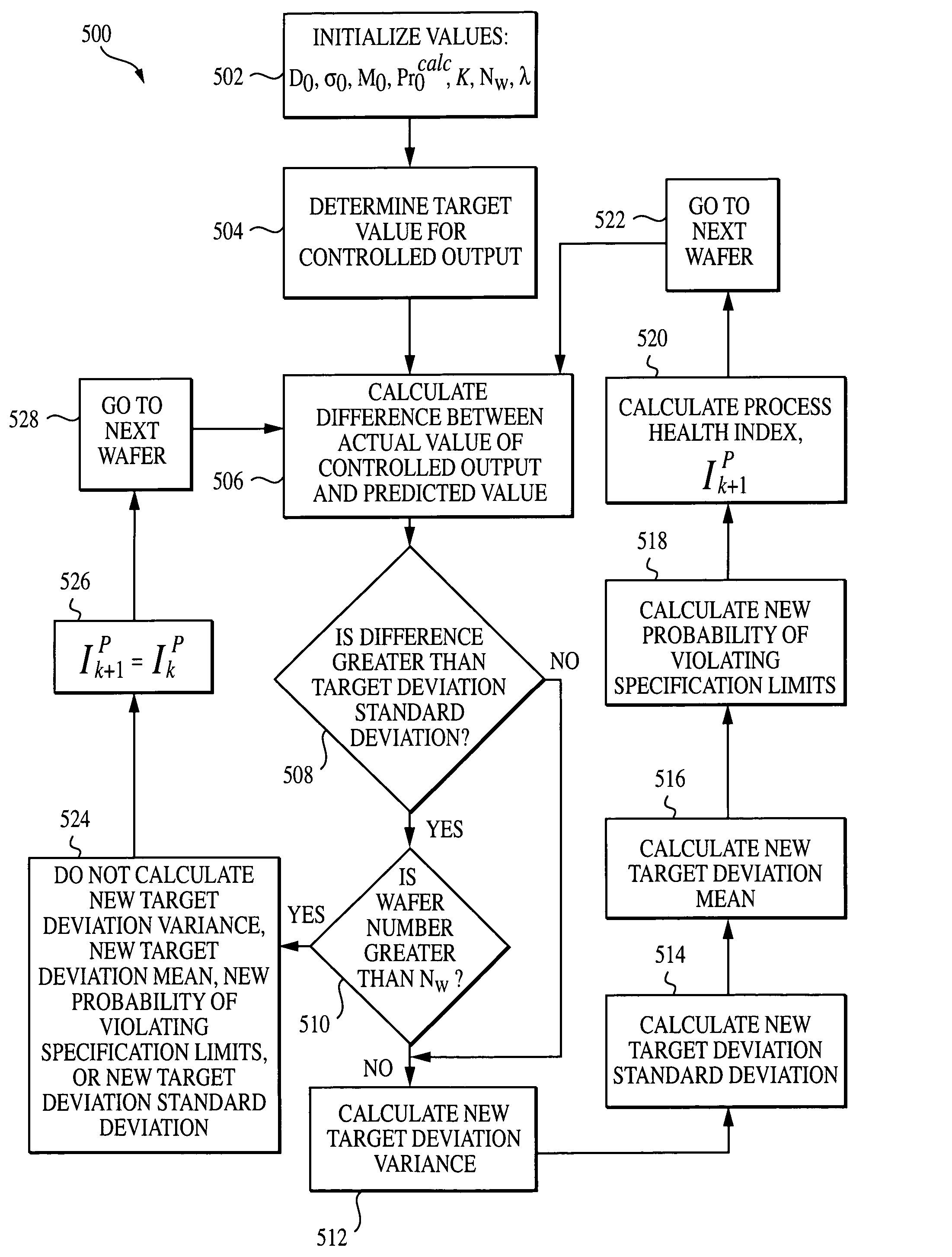
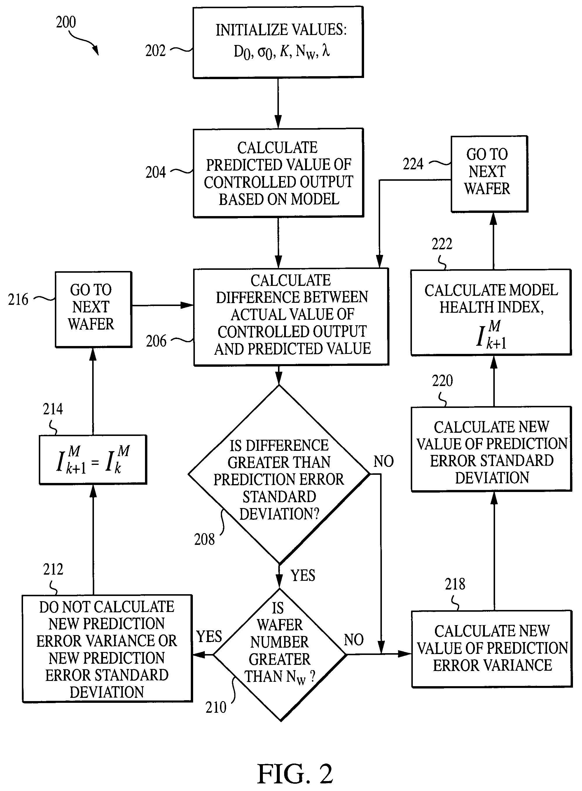
- The development of indices for model and process health monitoring, such as model health index and process health index, which estimate variance and bias, calculate probabilities of violating specification limits, and provide notifications when limits are exceeded, allowing for real-time monitoring and control of static processes like semiconductor manufacturing.

Cleanroom Standards and Semiconductor Manufacturing Regulations
Cleanroom standards for wafer thinning operations are governed by stringent international protocols, primarily ISO 14644 series and Federal Standard 209E. These standards establish critical parameters for airborne particle concentrations, with Class 1 cleanrooms requiring fewer than 10 particles per cubic foot of 0.5 micrometers or larger. For wafer thinning processes, Class 1 or Class 10 environments are typically mandated due to the extreme sensitivity of thinned wafers to contamination.
Semiconductor manufacturing regulations encompass multiple regulatory frameworks across different jurisdictions. In the United States, the Environmental Protection Agency (EPA) regulates chemical emissions and waste management, while the Occupational Safety and Health Administration (OSHA) oversees worker safety protocols. The European Union enforces REACH regulations for chemical substance management, and RoHS directives for hazardous substance restrictions in electronic components.
Specific regulatory requirements for particle control during wafer thinning include mandatory monitoring of volatile organic compounds (VOCs), implementation of advanced filtration systems, and adherence to strict chemical handling protocols. The regulations mandate continuous air quality monitoring with real-time particle counters and require documentation of all deviations from established cleanliness standards.
Compliance frameworks require comprehensive validation procedures for cleanroom performance, including regular certification of HEPA and ULPA filtration systems. Personnel training protocols must meet industry standards such as SEMI S2 and S8 guidelines, ensuring proper gowning procedures and contamination prevention techniques. Quality management systems must align with ISO 9001 and automotive industry standards like IATF 16949 for semiconductor applications.
Recent regulatory updates have introduced more stringent requirements for nanoscale particle detection and control, reflecting the industry's progression toward smaller feature sizes. These evolving standards necessitate advanced monitoring technologies and enhanced process control methodologies to maintain compliance while optimizing manufacturing efficiency in wafer thinning operations.
Environmental Impact Assessment of Thinning Processes
The environmental impact assessment of wafer thinning processes reveals significant concerns across multiple ecological dimensions. Traditional mechanical grinding and chemical etching methods generate substantial waste streams, including silicon particulates, chemical slurries, and contaminated process fluids. These byproducts pose immediate challenges for semiconductor facilities in terms of waste management, regulatory compliance, and long-term environmental stewardship.
Air quality impacts represent a primary concern in thinning operations. Mechanical processes release fine silicon particles and abrasive materials into the atmosphere, requiring sophisticated filtration systems to prevent workplace exposure and environmental contamination. Chemical thinning processes emit volatile organic compounds and acidic vapors, necessitating comprehensive air treatment infrastructure. The energy intensity of these mitigation systems contributes significantly to the overall carbon footprint of wafer processing facilities.
Water consumption and contamination present equally critical environmental challenges. Chemical thinning processes require substantial volumes of ultrapure water for rinsing and cleaning operations, placing stress on local water resources. The resulting wastewater contains heavy metals, acids, and organic solvents that require extensive treatment before discharge. Current treatment technologies, while effective, generate secondary waste streams and consume considerable energy, amplifying the environmental burden.
Solid waste generation from thinning processes includes spent abrasives, filter materials, and chemical sludges classified as hazardous waste. The disposal of these materials requires specialized handling and treatment facilities, often involving high-temperature incineration or secure landfill storage. The long-term environmental implications of these disposal methods raise concerns about soil and groundwater contamination.
Energy consumption patterns in thinning operations contribute substantially to greenhouse gas emissions. High-precision grinding equipment, chemical processing systems, and environmental control infrastructure demand continuous power supply. The carbon intensity varies significantly based on regional energy sources, with facilities in coal-dependent regions showing markedly higher environmental impact profiles compared to those utilizing renewable energy sources.
Emerging assessment methodologies incorporate lifecycle analysis approaches to quantify environmental impacts from raw material extraction through end-of-life disposal. These comprehensive evaluations reveal that environmental optimization requires integrated approaches addressing process efficiency, waste minimization, and energy conservation simultaneously rather than isolated improvements in individual impact categories.
Unlock deeper insights with PatSnap Eureka Quick Research — get a full tech report to explore trends and direct your research. Try now!
Generate Your Research Report Instantly with AI Agent
Supercharge your innovation with PatSnap Eureka AI Agent Platform!