Electromagnetic Waves in Advanced Photonics: Key Trends
JUL 11, 20259 MIN READ
Generate Your Research Report Instantly with AI Agent
Patsnap Eureka helps you evaluate technical feasibility & market potential.
Photonics Evolution
Photonics has undergone a remarkable evolution since its inception, driven by advancements in electromagnetic wave manipulation and control. The field has progressed from basic optical components to sophisticated integrated photonic systems, revolutionizing various industries and scientific disciplines.
In the early stages, photonics primarily focused on the development of fundamental optical elements such as lenses, mirrors, and prisms. These components formed the basis for manipulating light in simple optical systems. As technology advanced, the field expanded to include more complex devices like lasers and optical fibers, which became cornerstones of modern telecommunications and data transmission.
The advent of semiconductor technology in the mid-20th century marked a significant turning point in photonics. The invention of light-emitting diodes (LEDs) and semiconductor lasers opened up new possibilities for compact, efficient light sources. This paved the way for applications in displays, lighting, and optical storage devices.
Integrated photonics emerged as a game-changing concept in the late 20th century. By miniaturizing optical components and integrating them onto a single chip, researchers were able to create complex photonic circuits capable of processing light signals with unprecedented speed and efficiency. This development has been crucial in advancing optical computing and high-speed data communication.
Recent years have seen a surge in nanophotonics research, exploring light-matter interactions at the nanoscale. This has led to breakthroughs in areas such as plasmonics, metamaterials, and photonic crystals. These technologies enable precise control over electromagnetic waves at subwavelength scales, opening up possibilities for super-resolution imaging, cloaking devices, and enhanced sensing capabilities.
Quantum photonics has emerged as a frontier area, leveraging the quantum properties of light for applications in secure communication, quantum computing, and ultra-precise measurements. The development of single-photon sources, detectors, and quantum memories has been instrumental in advancing this field.
The convergence of photonics with other disciplines has further accelerated its evolution. Biophotonics, for instance, combines photonics with biology and medicine, leading to innovations in medical imaging, diagnostics, and therapies. Similarly, the integration of photonics with artificial intelligence and machine learning is driving advancements in optical neural networks and photonic computing architectures.
Looking ahead, the evolution of photonics is poised to continue at a rapid pace. Emerging trends include the development of all-optical signal processing, neuromorphic photonic computing, and the integration of photonics with other quantum technologies. These advancements promise to push the boundaries of what is possible in information processing, sensing, and communication, shaping the future of technology across multiple domains.
Market Demand Analysis
The market demand for advanced photonics technologies leveraging electromagnetic waves is experiencing significant growth across various sectors. This surge is primarily driven by the increasing need for high-speed data transmission, advanced sensing capabilities, and precise imaging technologies in industries such as telecommunications, healthcare, and defense.
In the telecommunications sector, the rollout of 5G networks and the anticipation of 6G technologies have created a robust demand for photonic components capable of handling higher frequencies and bandwidths. Optical transceivers, photonic integrated circuits, and advanced fiber optics are seeing increased adoption as telecom companies strive to meet the growing data traffic demands.
The healthcare industry is another major driver of market demand for electromagnetic wave-based photonics. Advanced imaging techniques such as optical coherence tomography (OCT) and photoacoustic imaging are gaining traction due to their non-invasive nature and high-resolution capabilities. These technologies are finding applications in ophthalmology, dermatology, and cancer diagnostics, contributing to the overall market growth.
In the defense and aerospace sectors, there is a rising demand for photonics-based sensing and imaging systems. LiDAR technology, which utilizes electromagnetic waves for 3D mapping and object detection, is becoming increasingly important for autonomous vehicles and drone navigation. Additionally, photonic sensors are being employed in military applications for threat detection and surveillance.
The industrial sector is also contributing to the market demand, with photonics playing a crucial role in advanced manufacturing processes. Laser-based material processing, machine vision systems, and quality control applications are driving the adoption of photonic technologies in smart factories and Industry 4.0 initiatives.
As environmental concerns grow, there is an increasing demand for photonics-based solutions in energy efficiency and renewable energy sectors. Photovoltaic technologies and advanced lighting systems are seeing significant market traction, driven by the global push towards sustainable energy solutions.
The consumer electronics market is another area where electromagnetic wave-based photonics is gaining ground. Augmented reality (AR) and virtual reality (VR) devices, as well as advanced display technologies, are creating new opportunities for photonics applications in consumer products.
Overall, the market for advanced photonics technologies is expected to continue its upward trajectory, with emerging applications in quantum computing, biosensing, and terahertz imaging further expanding the potential market size. As industries increasingly rely on high-performance optical and photonic systems, the demand for innovative solutions in electromagnetic wave manipulation is set to grow, driving research and development efforts in this field.
EM Wave Challenges
The field of advanced photonics faces several significant challenges in harnessing and controlling electromagnetic waves. One of the primary obstacles is the diffraction limit, which restricts the ability to focus light beyond a certain point, limiting the resolution of optical systems. This fundamental constraint has implications for various applications, including microscopy, lithography, and data storage.
Another critical challenge lies in the manipulation of light at the nanoscale. As photonic devices shrink to dimensions comparable to or smaller than the wavelength of light, traditional optical principles become less applicable. This necessitates the development of novel approaches to guide, confine, and process light at these extreme scales, often requiring the integration of photonics with other fields such as plasmonics and metamaterials.
The management of optical losses presents a persistent challenge in photonic systems. As light propagates through materials or structures, various mechanisms such as absorption, scattering, and radiation can lead to signal degradation. Minimizing these losses is crucial for improving the efficiency and performance of photonic devices, particularly in areas like optical communications and quantum information processing.
Nonlinear optical effects pose both challenges and opportunities in advanced photonics. While these effects can enable novel functionalities such as frequency conversion and all-optical switching, they also introduce complexities in system design and can lead to unwanted signal distortions. Harnessing and controlling nonlinear phenomena remains an active area of research and development.
The integration of photonics with electronics presents significant technical hurdles. Bridging the gap between these two domains is essential for realizing high-performance, energy-efficient systems that can leverage the strengths of both optical and electronic technologies. This integration requires overcoming challenges related to material compatibility, fabrication processes, and system-level design.
Thermal management is another critical issue in photonic systems, particularly as device densities increase and power levels rise. Heat generation can affect the performance and reliability of photonic components, necessitating innovative cooling strategies and thermally robust designs.
Lastly, the development of tunable and reconfigurable photonic systems remains a significant challenge. The ability to dynamically control the properties of optical components and systems is crucial for adaptive and multifunctional devices. This requires advancements in materials science, actuation mechanisms, and control systems to enable rapid and precise manipulation of electromagnetic waves in photonic structures.
Current EM Solutions
01 Electromagnetic wave detection and measurement
Various devices and methods for detecting and measuring electromagnetic waves are described. These include sensors, antennas, and specialized equipment designed to capture and analyze electromagnetic signals across different frequencies and intensities.- Electromagnetic wave detection and measurement: Various devices and methods for detecting and measuring electromagnetic waves are described. These include sensors, antennas, and other specialized equipment designed to capture and analyze electromagnetic signals across different frequencies and intensities.
- Electromagnetic wave shielding and protection: Technologies for shielding and protecting against electromagnetic waves are presented. These involve materials and structures designed to block or absorb electromagnetic radiation, protecting sensitive equipment or living organisms from potential harmful effects.
- Electromagnetic wave communication systems: Advancements in communication systems utilizing electromagnetic waves are discussed. These include improvements in wireless transmission, reception, and processing of electromagnetic signals for various applications such as mobile networks and satellite communications.
- Electromagnetic wave energy harvesting: Innovative methods for harvesting energy from electromagnetic waves are explored. These technologies aim to capture and convert ambient electromagnetic radiation into usable electrical energy for powering devices or supplementing existing power sources.
- Electromagnetic wave applications in medical field: The use of electromagnetic waves in medical applications is examined. This includes diagnostic imaging techniques, therapeutic treatments, and monitoring systems that leverage various frequencies of electromagnetic radiation for healthcare purposes.
02 Electromagnetic wave shielding and protection
Technologies for shielding and protecting against electromagnetic waves are presented. These involve materials and structures designed to block or absorb electromagnetic radiation, protecting sensitive equipment or living organisms from potential harmful effects.Expand Specific Solutions03 Electromagnetic wave communication systems
Advancements in communication systems utilizing electromagnetic waves are discussed. These include improvements in wireless communication technologies, signal processing techniques, and novel methods for transmitting and receiving electromagnetic signals.Expand Specific Solutions04 Electromagnetic wave energy harvesting
Innovations in harvesting energy from electromagnetic waves are explored. These technologies aim to capture and convert ambient electromagnetic radiation into usable electrical energy, potentially providing power for various applications.Expand Specific Solutions05 Electromagnetic wave applications in medical field
The use of electromagnetic waves in medical applications is discussed. This includes diagnostic imaging techniques, therapeutic treatments, and monitoring systems that utilize various forms of electromagnetic radiation to improve healthcare outcomes.Expand Specific Solutions
Industry Leaders
The electromagnetic waves in advanced photonics field is experiencing rapid growth and innovation, driven by increasing demand for high-performance optical technologies. The market is in a dynamic phase, with significant potential for expansion across various applications. Key players like Canon, Sony, and Mitsubishi Electric are investing heavily in R&D to maintain their competitive edge. Emerging companies and research institutions, such as Harbin Institute of Technology and Shanghai Jiao Tong University, are also making notable contributions. The technology is maturing, but there's still room for breakthrough innovations, particularly in areas like nanophotonics and quantum optics. Collaboration between industry leaders and academic institutions is accelerating progress, indicating a promising future for this sector.
The Regents of the University of California
Technical Solution: The University of California has made significant advancements in electromagnetic waves for advanced photonics. They have developed a novel metamaterial-based approach to manipulate light at the nanoscale, enabling unprecedented control over electromagnetic waves[1]. Their research focuses on creating artificial nanostructures that can bend, shape, and focus light in ways not possible with natural materials. This includes the development of metasurfaces, which are ultra-thin planar devices capable of molding optical wavefronts into arbitrary shapes[2]. These metasurfaces have applications in beam steering, holography, and optical computing. Additionally, the university has pioneered work in plasmonics, utilizing the interaction between light and free electrons in metals to create highly confined electromagnetic fields[3]. This technology has potential applications in ultra-compact optical devices and high-resolution imaging systems.
Strengths: Cutting-edge research in metamaterials and plasmonics, strong interdisciplinary collaboration. Weaknesses: Potential challenges in scaling up for commercial production, high costs associated with nanofabrication processes.
Hewlett Packard Enterprise Development LP
Technical Solution: Hewlett Packard Enterprise (HPE) has been at the forefront of developing advanced photonic technologies for data centers and high-performance computing. Their focus is on silicon photonics, which integrates optical components with traditional silicon-based electronics[4]. HPE has developed photonic integrated circuits (PICs) that use light for data transmission, significantly increasing bandwidth and reducing energy consumption compared to traditional electronic systems. Their technology includes on-chip lasers, modulators, and detectors, enabling high-speed optical interconnects within and between computer systems[5]. HPE's photonic memory cube (PMC) technology combines photonic interconnects with 3D stacked memory, offering unprecedented memory bandwidth and reduced latency for data-intensive applications[6]. They are also exploring the use of electromagnetic waves in quantum computing, developing optical quantum circuits for potential quantum information processing applications.
Strengths: Strong integration with existing computing infrastructure, potential for significant performance improvements in data centers. Weaknesses: High initial costs, challenges in transitioning from electronic to photonic systems in existing infrastructure.
Key EM Wave Patents
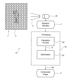
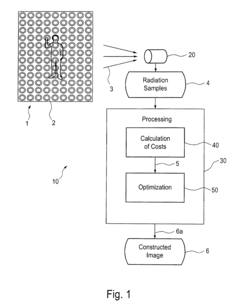
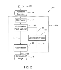
Passive radiometric imaging device and method
PatentInactiveUS20120188118A1
Innovation
- A passive radiometric imaging device and method that processes radiation samples using a cost calculation unit and optimization unit to determine pixel values, considering the piece-wise smooth nature of radiometric surfaces, with an energy function that accounts for noise levels and neighboring samples to reconstruct images with improved quality.
Photonic devices having degenerate spectral band edges and methods for using the same
PatentActiveUS20110176771A1
Innovation
- A photonic device configured to display a degenerate band edge, utilizing a periodic structure with misaligned anisotropic layers that converts incident electromagnetic waves into a frozen mode with enhanced amplitude and compressed pulse length, allowing for complete conversion of radiation into a slow mode with smaller dimensions.
Quantum Integration
The integration of quantum mechanics with electromagnetic wave theory in advanced photonics represents a significant frontier in modern physics and engineering. This convergence has led to groundbreaking developments in quantum optics and quantum information processing, pushing the boundaries of our understanding and control of light-matter interactions at the quantum level.
One of the key trends in this field is the development of quantum photonic integrated circuits (QPICs). These circuits aim to manipulate and process quantum states of light on a chip-scale platform, offering unprecedented capabilities for quantum computing and communication. The integration of single-photon sources, quantum memories, and detectors on a single chip is a major focus of current research efforts.
Another important trend is the exploration of quantum metamaterials. These artificially engineered structures leverage quantum mechanical effects to manipulate electromagnetic waves in ways not possible with conventional materials. Quantum metamaterials have the potential to enable novel optical devices with extraordinary properties, such as perfect absorption, superlensing, and cloaking at the quantum level.
The study of quantum plasmonics is also gaining momentum. This field investigates the quantum properties of surface plasmons, which are collective oscillations of electrons at metal-dielectric interfaces. Quantum plasmonics offers the possibility of confining and manipulating light at nanoscale dimensions, far beyond the diffraction limit, with applications in sensing, imaging, and quantum information processing.
Quantum-enhanced sensing and metrology represent another significant trend in the integration of quantum mechanics with electromagnetic waves. By exploiting quantum entanglement and superposition, researchers are developing sensors and measurement techniques that can surpass classical limits of precision and sensitivity. This has profound implications for fields such as gravitational wave detection, atomic clocks, and magnetic field sensing.
The development of topological photonics is also at the forefront of quantum integration in advanced photonics. This field explores the application of topological concepts from condensed matter physics to optical systems, leading to the creation of robust, unidirectional light propagation channels that are protected against scattering and defects. Topological photonic systems offer new possibilities for creating quantum optical circuits with enhanced stability and efficiency.
As these trends continue to evolve, the integration of quantum mechanics with electromagnetic wave theory is expected to drive innovations in quantum technologies, opening up new avenues for secure communication, ultra-precise sensing, and quantum computing. The interdisciplinary nature of this field, combining physics, engineering, and materials science, promises to yield transformative advances in our ability to harness and control light at the most fundamental level.
Photonic Computing
Photonic computing represents a paradigm shift in information processing, leveraging the unique properties of light to perform computational tasks. This emerging technology holds the promise of overcoming the limitations of traditional electronic computing, particularly in terms of speed, energy efficiency, and bandwidth.
At the core of photonic computing is the manipulation of electromagnetic waves in the optical spectrum. These waves are used to encode, transmit, and process information, offering several advantages over electronic signals. The high frequencies of light allow for faster data transmission and processing, potentially enabling computations at speeds approaching the speed of light.
One of the key trends in photonic computing is the development of integrated photonic circuits. These circuits combine multiple optical components on a single chip, analogous to electronic integrated circuits. They include elements such as waveguides, modulators, detectors, and optical sources, all working together to perform complex operations using light.
Another significant trend is the exploration of novel materials for photonic devices. Materials with unique optical properties, such as nonlinear optical materials and photonic crystals, are being investigated for their potential to enhance the performance of photonic computing systems. These materials can manipulate light in ways that enable more efficient and compact photonic circuits.
The integration of photonics with existing electronic systems is also a crucial area of development. Hybrid electro-optical systems aim to combine the strengths of both technologies, leveraging the high-speed processing capabilities of photonics with the mature infrastructure of electronics. This approach is particularly relevant for applications in data centers and high-performance computing.
Quantum photonics is another frontier in the field, exploring the use of single photons and quantum states of light for computing. This area holds promise for quantum information processing and secure communication systems, potentially revolutionizing fields such as cryptography and complex problem-solving.
As research in photonic computing progresses, we are seeing advancements in optical neural networks and optical machine learning architectures. These systems aim to perform AI and machine learning tasks using optical components, potentially offering significant speed and energy efficiency improvements over their electronic counterparts.
The development of photonic computing technologies is closely tied to advancements in nanophotonics and metamaterials. These fields enable the precise control and manipulation of light at the nanoscale, opening up new possibilities for compact and efficient photonic devices.
Unlock deeper insights with Patsnap Eureka Quick Research — get a full tech report to explore trends and direct your research. Try now!
Generate Your Research Report Instantly with AI Agent
Supercharge your innovation with Patsnap Eureka AI Agent Platform!