

Enhancing Stability in Microbump Arrays for Edge Deployment
APR 22, 20269 MIN READ
Generate Your Research Report Instantly with AI Agent
PatSnap Eureka helps you evaluate technical feasibility & market potential.
Microbump Array Technology Background and Stability Goals
Microbump arrays represent a critical interconnect technology that has evolved significantly since their introduction in the early 2000s. Originally developed as a solution for high-density chip-to-chip connections, these microscale solder bumps typically measure between 10-50 micrometers in diameter and enable direct electrical connections between semiconductor devices. The technology emerged from the need to overcome limitations of traditional wire bonding and flip-chip packaging, particularly in applications requiring miniaturization and high I/O density.
The evolution of microbump technology has been driven by the semiconductor industry's relentless pursuit of Moore's Law and the increasing demand for system-in-package (SiP) solutions. Early implementations focused primarily on memory stacking applications, where multiple DRAM dies were vertically integrated using through-silicon vias (TSVs) and microbump interconnects. This approach enabled significant reductions in package footprint while maintaining or improving electrical performance compared to traditional packaging methods.
Edge deployment applications have introduced unique challenges that distinguish them from traditional data center or consumer electronics environments. Edge computing devices must operate reliably in harsh conditions including extreme temperatures, vibration, humidity variations, and limited maintenance accessibility. These environmental stressors place unprecedented demands on microbump array stability, as interconnect failures can result in complete system malfunction in mission-critical applications.
The primary stability goals for microbump arrays in edge deployment center on achieving long-term reliability under thermal cycling, mechanical stress resistance, and maintaining electrical integrity throughout extended operational periods. Thermal cycling represents one of the most significant challenges, as coefficient of thermal expansion mismatches between different materials in the stack can induce mechanical stress at microbump interfaces. The target reliability metrics typically require survival of 1000-3000 thermal cycles between -40°C and +125°C without degradation in electrical performance.
Mechanical stability goals encompass resistance to shock and vibration loads commonly encountered in automotive, industrial IoT, and telecommunications infrastructure applications. The microbump arrays must maintain structural integrity under acceleration forces up to 1500G for shock events and sustained vibration frequencies ranging from 10Hz to 2000Hz. Additionally, the interconnects must demonstrate consistent electrical characteristics with contact resistance remaining below 50 milliohms and maintaining signal integrity for high-speed digital communications.
Current stability objectives also emphasize the need for predictable aging behavior and failure modes that enable condition monitoring and predictive maintenance strategies. This includes developing microbump designs that exhibit gradual performance degradation rather than catastrophic failure, allowing edge systems to implement graceful degradation protocols when interconnect reliability begins to decline.
The evolution of microbump technology has been driven by the semiconductor industry's relentless pursuit of Moore's Law and the increasing demand for system-in-package (SiP) solutions. Early implementations focused primarily on memory stacking applications, where multiple DRAM dies were vertically integrated using through-silicon vias (TSVs) and microbump interconnects. This approach enabled significant reductions in package footprint while maintaining or improving electrical performance compared to traditional packaging methods.
Edge deployment applications have introduced unique challenges that distinguish them from traditional data center or consumer electronics environments. Edge computing devices must operate reliably in harsh conditions including extreme temperatures, vibration, humidity variations, and limited maintenance accessibility. These environmental stressors place unprecedented demands on microbump array stability, as interconnect failures can result in complete system malfunction in mission-critical applications.
The primary stability goals for microbump arrays in edge deployment center on achieving long-term reliability under thermal cycling, mechanical stress resistance, and maintaining electrical integrity throughout extended operational periods. Thermal cycling represents one of the most significant challenges, as coefficient of thermal expansion mismatches between different materials in the stack can induce mechanical stress at microbump interfaces. The target reliability metrics typically require survival of 1000-3000 thermal cycles between -40°C and +125°C without degradation in electrical performance.
Mechanical stability goals encompass resistance to shock and vibration loads commonly encountered in automotive, industrial IoT, and telecommunications infrastructure applications. The microbump arrays must maintain structural integrity under acceleration forces up to 1500G for shock events and sustained vibration frequencies ranging from 10Hz to 2000Hz. Additionally, the interconnects must demonstrate consistent electrical characteristics with contact resistance remaining below 50 milliohms and maintaining signal integrity for high-speed digital communications.
Current stability objectives also emphasize the need for predictable aging behavior and failure modes that enable condition monitoring and predictive maintenance strategies. This includes developing microbump designs that exhibit gradual performance degradation rather than catastrophic failure, allowing edge systems to implement graceful degradation protocols when interconnect reliability begins to decline.
Market Demand for Reliable Edge Computing Solutions
The global edge computing market is experiencing unprecedented growth driven by the proliferation of IoT devices, autonomous systems, and real-time applications requiring ultra-low latency processing. Industries ranging from manufacturing and healthcare to telecommunications and automotive are increasingly deploying edge infrastructure to process data closer to its source, reducing bandwidth costs and improving response times.
Critical applications in autonomous vehicles, industrial automation, and medical devices demand exceptional reliability from edge computing hardware. System failures in these environments can result in significant safety risks, operational disruptions, and financial losses. The reliability requirements for edge deployments often exceed those of traditional data center environments, as edge devices typically operate in harsh conditions with limited maintenance access.
Microbump array technology serves as a fundamental interconnect solution in advanced semiconductor packaging for edge computing processors. These microscopic solder connections enable high-density chip-to-substrate connections essential for compact, high-performance edge devices. However, the mechanical stress from thermal cycling, vibration, and environmental factors in edge deployments poses significant challenges to microbump stability and long-term reliability.
The market demand for enhanced microbump stability is particularly acute in sectors deploying edge computing at scale. Telecommunications companies rolling out 5G infrastructure require edge servers with guaranteed uptime exceeding industry standards. Manufacturing facilities implementing Industry 4.0 solutions need edge devices capable of continuous operation in temperature-variable environments without degradation.
Current market trends indicate a shift toward more stringent reliability specifications for edge computing hardware. Customers are increasingly willing to invest in premium solutions that demonstrate superior long-term stability, recognizing that the total cost of ownership includes not just initial hardware costs but also maintenance, replacement, and downtime expenses.
The convergence of artificial intelligence workloads at the edge further amplifies the demand for stable microbump arrays. AI inference chips require consistent electrical performance to maintain accuracy, making connection reliability a critical factor in market acceptance and commercial viability of edge AI solutions.
Critical applications in autonomous vehicles, industrial automation, and medical devices demand exceptional reliability from edge computing hardware. System failures in these environments can result in significant safety risks, operational disruptions, and financial losses. The reliability requirements for edge deployments often exceed those of traditional data center environments, as edge devices typically operate in harsh conditions with limited maintenance access.
Microbump array technology serves as a fundamental interconnect solution in advanced semiconductor packaging for edge computing processors. These microscopic solder connections enable high-density chip-to-substrate connections essential for compact, high-performance edge devices. However, the mechanical stress from thermal cycling, vibration, and environmental factors in edge deployments poses significant challenges to microbump stability and long-term reliability.
The market demand for enhanced microbump stability is particularly acute in sectors deploying edge computing at scale. Telecommunications companies rolling out 5G infrastructure require edge servers with guaranteed uptime exceeding industry standards. Manufacturing facilities implementing Industry 4.0 solutions need edge devices capable of continuous operation in temperature-variable environments without degradation.
Current market trends indicate a shift toward more stringent reliability specifications for edge computing hardware. Customers are increasingly willing to invest in premium solutions that demonstrate superior long-term stability, recognizing that the total cost of ownership includes not just initial hardware costs but also maintenance, replacement, and downtime expenses.
The convergence of artificial intelligence workloads at the edge further amplifies the demand for stable microbump arrays. AI inference chips require consistent electrical performance to maintain accuracy, making connection reliability a critical factor in market acceptance and commercial viability of edge AI solutions.
Current Microbump Stability Issues and Technical Challenges
Microbump arrays face significant stability challenges when deployed in edge computing environments, where harsh operating conditions and stringent reliability requirements create unique technical obstacles. The primary stability issues stem from thermal cycling stress, mechanical fatigue, and environmental degradation that occur during extended field operations.
Thermal cycling represents one of the most critical challenges affecting microbump stability. Edge devices frequently experience rapid temperature fluctuations ranging from -40°C to 85°C, causing differential thermal expansion between silicon dies and substrates. This thermal mismatch generates cyclic stress concentrations at microbump interfaces, leading to crack initiation and propagation. The coefficient of thermal expansion mismatch between different materials in the interconnect stack creates shear stress that accumulates over thousands of thermal cycles.
Mechanical reliability issues arise from the inherent size constraints of microbump structures. With bump diameters typically ranging from 20 to 40 micrometers and pitches below 50 micrometers, the reduced cross-sectional area limits current-carrying capacity and increases current density. High current density leads to electromigration phenomena, where metal atoms migrate along the direction of electron flow, causing void formation and eventual interconnect failure.
Solder joint fatigue constitutes another major technical challenge, particularly in high-vibration edge deployment scenarios. The small volume of solder in microbumps provides limited compliance to accommodate stress, making them more susceptible to low-cycle fatigue failure compared to larger conventional solder joints. The brittle nature of intermetallic compounds formed during reflow processes further reduces the mechanical robustness of these connections.
Environmental factors specific to edge deployments exacerbate stability problems. Humidity variations cause hygroscopic swelling in underfill materials, creating additional mechanical stress on microbump arrays. Corrosive atmospheres in industrial environments can lead to oxidation and degradation of exposed metallization layers, compromising electrical conductivity and mechanical integrity.
Manufacturing variability presents ongoing challenges in achieving consistent microbump reliability. Process variations in bump height, diameter, and placement accuracy create non-uniform stress distributions across arrays. Incomplete wetting during reflow processes results in weak solder joints with reduced mechanical strength and increased electrical resistance.
The scaling trend toward finer pitch microbump arrays intensifies these stability challenges. As bump spacing decreases below 40 micrometers, crosstalk between adjacent interconnects increases, while the reduced standoff height limits underfill flow and creates potential delamination sites. These geometric constraints make it increasingly difficult to maintain long-term reliability in demanding edge computing applications.
Thermal cycling represents one of the most critical challenges affecting microbump stability. Edge devices frequently experience rapid temperature fluctuations ranging from -40°C to 85°C, causing differential thermal expansion between silicon dies and substrates. This thermal mismatch generates cyclic stress concentrations at microbump interfaces, leading to crack initiation and propagation. The coefficient of thermal expansion mismatch between different materials in the interconnect stack creates shear stress that accumulates over thousands of thermal cycles.
Mechanical reliability issues arise from the inherent size constraints of microbump structures. With bump diameters typically ranging from 20 to 40 micrometers and pitches below 50 micrometers, the reduced cross-sectional area limits current-carrying capacity and increases current density. High current density leads to electromigration phenomena, where metal atoms migrate along the direction of electron flow, causing void formation and eventual interconnect failure.
Solder joint fatigue constitutes another major technical challenge, particularly in high-vibration edge deployment scenarios. The small volume of solder in microbumps provides limited compliance to accommodate stress, making them more susceptible to low-cycle fatigue failure compared to larger conventional solder joints. The brittle nature of intermetallic compounds formed during reflow processes further reduces the mechanical robustness of these connections.
Environmental factors specific to edge deployments exacerbate stability problems. Humidity variations cause hygroscopic swelling in underfill materials, creating additional mechanical stress on microbump arrays. Corrosive atmospheres in industrial environments can lead to oxidation and degradation of exposed metallization layers, compromising electrical conductivity and mechanical integrity.
Manufacturing variability presents ongoing challenges in achieving consistent microbump reliability. Process variations in bump height, diameter, and placement accuracy create non-uniform stress distributions across arrays. Incomplete wetting during reflow processes results in weak solder joints with reduced mechanical strength and increased electrical resistance.
The scaling trend toward finer pitch microbump arrays intensifies these stability challenges. As bump spacing decreases below 40 micrometers, crosstalk between adjacent interconnects increases, while the reduced standoff height limits underfill flow and creates potential delamination sites. These geometric constraints make it increasingly difficult to maintain long-term reliability in demanding edge computing applications.
Existing Microbump Stability Enhancement Solutions
01 Microbump structure design and geometry optimization
The stability of microbump arrays can be enhanced through optimized structural design, including controlling the height-to-diameter ratio, pitch spacing, and geometric configuration of the bumps. Proper dimensional control and uniform distribution patterns help prevent mechanical failure and improve structural integrity during thermal cycling and mechanical stress. Advanced designs may incorporate tapered profiles or reinforced base structures to enhance resistance to shear forces and improve overall array stability.- Microbump structure design and geometry optimization: The stability of microbump arrays can be enhanced through optimized structural design, including control of bump height, diameter, pitch, and aspect ratio. Proper geometric configurations help distribute mechanical stress more evenly and reduce the risk of structural failure. Design considerations also include the shape profile of the bumps and their arrangement patterns to maximize mechanical stability and reliability during thermal cycling and mechanical loading.
- Material selection and composition for enhanced stability: The choice of materials for microbump arrays significantly impacts their mechanical and thermal stability. Various metal compositions, alloys, and multi-layer structures can be employed to improve resistance to electromigration, thermal stress, and mechanical fatigue. Material properties such as ductility, thermal expansion coefficient matching, and interfacial adhesion strength are critical factors in ensuring long-term stability of the microbump interconnections.
- Underfill and encapsulation techniques: The application of underfill materials and encapsulation methods plays a crucial role in stabilizing microbump arrays by providing mechanical support and stress redistribution. These materials fill the gaps between bumps and substrates, reducing the coefficient of thermal expansion mismatch and protecting the interconnections from environmental factors. Proper underfill flow characteristics and curing processes are essential for achieving uniform coverage and optimal mechanical reinforcement.
- Manufacturing process control and quality assurance: Precise control of manufacturing processes is essential for achieving stable microbump arrays. This includes optimization of deposition techniques, reflow processes, bonding parameters, and surface preparation methods. Process monitoring and quality control measures help ensure uniformity in bump formation, proper interfacial bonding, and minimal defects that could compromise stability. Advanced manufacturing techniques can reduce void formation and improve the consistency of bump characteristics across the array.
- Reliability testing and failure analysis methods: Comprehensive reliability testing methodologies are employed to evaluate and ensure the stability of microbump arrays under various stress conditions. These include thermal cycling tests, mechanical shock testing, and accelerated aging studies. Failure analysis techniques help identify potential weak points in the structure and guide improvements in design and manufacturing. Testing protocols assess parameters such as electrical resistance changes, mechanical integrity, and interfacial delamination to predict long-term performance and stability.
02 Material composition and metallurgical properties
The selection of appropriate materials and control of metallurgical properties are critical for microbump stability. This includes the use of specific metal alloys, intermetallic compound formation control, and optimization of material layers to prevent electromigration and reduce stress-induced failures. Material systems may incorporate barrier layers and diffusion-resistant compositions to maintain structural integrity over extended operational periods and temperature variations.Expand Specific Solutions03 Underfill and encapsulation techniques
Stability enhancement through underfill materials and encapsulation methods provides mechanical support and stress redistribution for microbump arrays. These techniques involve filling the gaps between bumps with polymer materials that cure to form a protective matrix, reducing thermal expansion mismatch effects and preventing moisture ingress. Advanced formulations can improve adhesion, control coefficient of thermal expansion, and enhance resistance to thermal cycling fatigue.Expand Specific Solutions04 Manufacturing process control and quality assurance
Precise control of fabrication processes is essential for achieving stable microbump arrays. This includes optimization of deposition techniques, reflow conditions, and surface preparation methods to ensure uniform bump formation and consistent interconnection quality. Process monitoring and inspection methods help identify defects early and maintain dimensional accuracy, while controlled atmosphere processing and temperature profiling prevent oxidation and ensure proper metallurgical bonding.Expand Specific Solutions05 Reliability testing and failure analysis methods
Comprehensive reliability assessment techniques are employed to evaluate and ensure microbump array stability under various stress conditions. These methods include accelerated thermal cycling tests, electromigration testing, and mechanical stress analysis to predict long-term performance. Advanced characterization techniques enable identification of failure modes, allowing for design improvements and process optimization to enhance overall reliability and operational lifetime of the interconnection structures.Expand Specific Solutions
Key Players in Advanced Packaging and Edge Computing
The microbump array stability technology for edge deployment represents an emerging sector within the broader semiconductor packaging industry, currently in its early-to-mid development stage with significant growth potential driven by increasing edge computing demands. The market shows substantial expansion opportunities as organizations deploy more distributed computing infrastructure requiring robust, miniaturized interconnect solutions. Technology maturity varies considerably across market participants, with established players like Samsung Electronics, IBM, and Siemens AG leveraging decades of semiconductor and industrial automation expertise to develop advanced packaging solutions. Research institutions including Caltech, Shanghai Jiao Tong University, and Imec contribute fundamental research breakthroughs, while specialized companies like STATS ChipPAC focus on packaging innovations. The competitive landscape features a mix of semiconductor giants, automotive manufacturers like Mercedes-Benz requiring reliable edge computing components, and emerging technology firms, creating a dynamic ecosystem where traditional packaging expertise intersects with next-generation edge deployment requirements.
International Business Machines Corp.
Technical Solution: IBM has developed advanced microbump interconnect technologies focusing on thermal-mechanical reliability enhancement through optimized solder compositions and underfill materials. Their approach utilizes copper pillar microbumps with controlled collapse chip connection (C4) technology, incorporating stress-buffer layers and thermal interface materials to mitigate coefficient of thermal expansion (CTE) mismatch between different materials. The company has implemented machine learning algorithms to predict failure modes and optimize bump placement patterns for improved mechanical stability under thermal cycling conditions.
Strengths: Extensive R&D capabilities and proven track record in semiconductor packaging. Weaknesses: High implementation costs and complex manufacturing processes.
Interuniversitair Micro-Electronica Centrum VZW
Technical Solution: IMEC has developed innovative microbump stability solutions through advanced materials engineering and process optimization. Their research focuses on novel bump metallurgy including nickel-gold surface finishes, optimized reflow profiles, and implementation of stress-relief structures. The center has pioneered the use of through-silicon via (TSV) integration with microbump arrays, developing comprehensive reliability testing methodologies including accelerated thermal cycling, mechanical shock testing, and electromigration analysis to ensure long-term stability in edge deployment scenarios.
Strengths: Cutting-edge research capabilities and strong industry partnerships for technology transfer. Weaknesses: Limited large-scale manufacturing experience and higher development timelines.
Core Innovations in Microbump Reliability Technologies
Microelectronic device connection structure
PatentInactiveUS7501708B2
Innovation
- A current dispersing structure using electrically insulating materials, such as silicon dioxide or polymide, is integrated within the interface portion, interface element, and interface region of the metal and solder elements, with protrusions or holes to spatially disperse current and enhance mechanical adhesion, reducing current crowding and electromigration.


Semiconductor integrated circuit and electronic apparatus having the same
PatentInactiveUS20050062151A1
Innovation
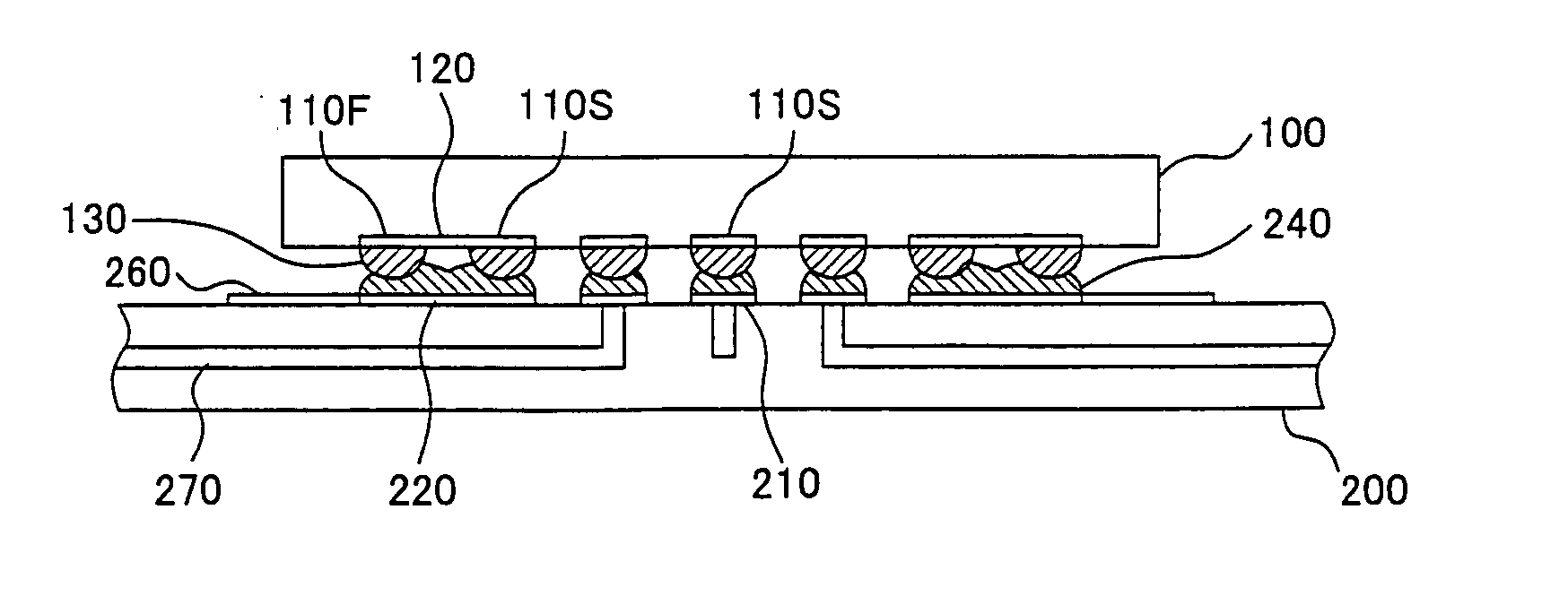
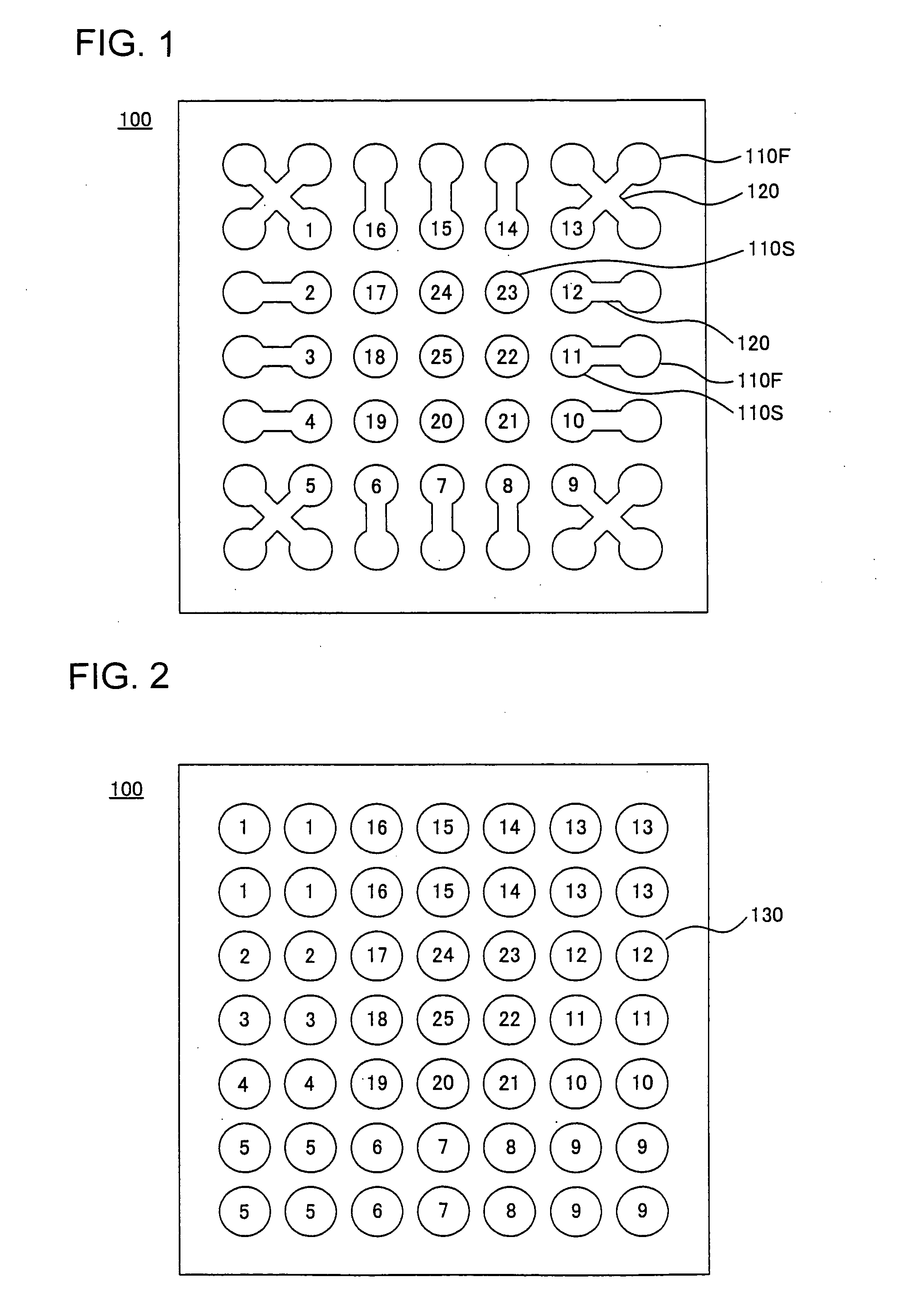
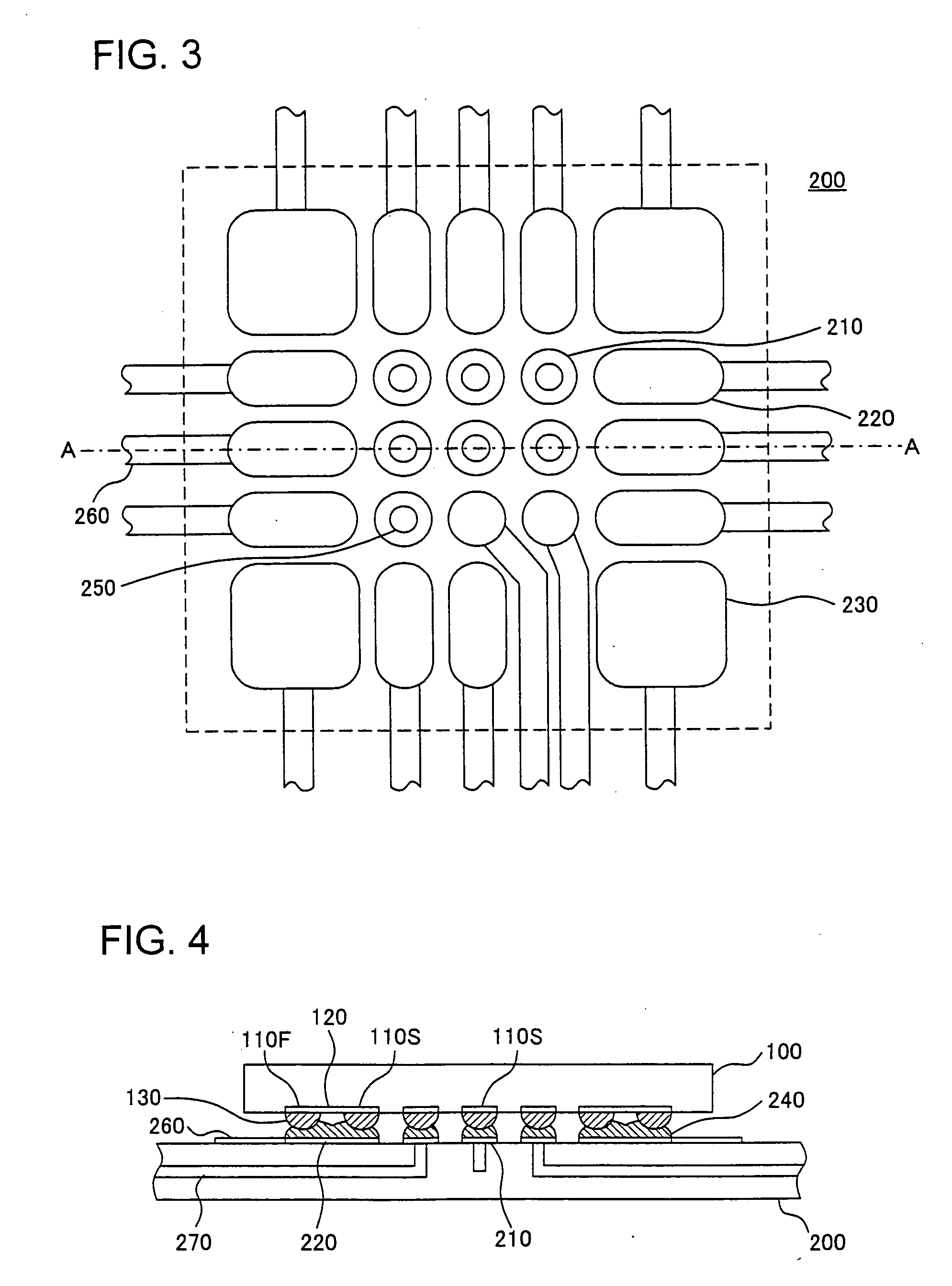
- The implementation of a grid array configuration with uniformly sized pads and bumps, where outermost pads serve as reinforcing pads connected to inner pads via inter-pad lead wires, providing uniform mechanical strength and simplifying manufacturing by using the same shape for all bumps.

Thermal Management Strategies for Edge Applications
Thermal management represents a critical challenge for microbump arrays deployed in edge computing environments, where space constraints and power limitations demand innovative cooling solutions. Edge devices typically operate in uncontrolled thermal environments with limited airflow and compact form factors, making traditional cooling methods inadequate for maintaining optimal junction temperatures in high-density interconnect structures.
Advanced thermal interface materials play a pivotal role in enhancing heat dissipation from microbump arrays. Phase change materials and thermally conductive polymers offer superior thermal conductivity while maintaining mechanical flexibility to accommodate thermal expansion mismatches. These materials can be integrated directly into the underfill process, creating dual-function solutions that provide both mechanical stability and thermal pathways.
Microfluidic cooling systems emerge as promising solutions for edge applications, utilizing miniaturized channels embedded within the substrate or package structure. These systems can achieve targeted cooling of hotspot regions while consuming minimal power, making them suitable for battery-operated edge devices. The integration of microfluidic networks requires careful consideration of flow dynamics and pressure drop optimization to ensure uniform temperature distribution across the microbump array.
Heat spreader technologies specifically designed for edge deployment focus on lightweight, low-profile solutions that maximize surface area for natural convection cooling. Graphene-enhanced thermal spreaders and vapor chamber technologies scaled for compact applications demonstrate significant improvements in thermal performance while maintaining the size constraints essential for edge device integration.
Thermal-aware design methodologies incorporate predictive modeling to optimize microbump placement and density based on anticipated thermal loads. These approaches utilize finite element analysis to identify optimal thermal pathways and minimize temperature gradients that could compromise solder joint reliability. Advanced simulation tools enable designers to evaluate multiple thermal management strategies during the design phase, reducing the need for extensive physical prototyping.
Smart thermal management systems leverage embedded temperature sensors and adaptive cooling control to dynamically respond to varying thermal loads in edge applications. These systems can modulate cooling intensity based on real-time thermal feedback, optimizing energy efficiency while maintaining critical temperature thresholds for microbump array stability.
Advanced thermal interface materials play a pivotal role in enhancing heat dissipation from microbump arrays. Phase change materials and thermally conductive polymers offer superior thermal conductivity while maintaining mechanical flexibility to accommodate thermal expansion mismatches. These materials can be integrated directly into the underfill process, creating dual-function solutions that provide both mechanical stability and thermal pathways.
Microfluidic cooling systems emerge as promising solutions for edge applications, utilizing miniaturized channels embedded within the substrate or package structure. These systems can achieve targeted cooling of hotspot regions while consuming minimal power, making them suitable for battery-operated edge devices. The integration of microfluidic networks requires careful consideration of flow dynamics and pressure drop optimization to ensure uniform temperature distribution across the microbump array.
Heat spreader technologies specifically designed for edge deployment focus on lightweight, low-profile solutions that maximize surface area for natural convection cooling. Graphene-enhanced thermal spreaders and vapor chamber technologies scaled for compact applications demonstrate significant improvements in thermal performance while maintaining the size constraints essential for edge device integration.
Thermal-aware design methodologies incorporate predictive modeling to optimize microbump placement and density based on anticipated thermal loads. These approaches utilize finite element analysis to identify optimal thermal pathways and minimize temperature gradients that could compromise solder joint reliability. Advanced simulation tools enable designers to evaluate multiple thermal management strategies during the design phase, reducing the need for extensive physical prototyping.
Smart thermal management systems leverage embedded temperature sensors and adaptive cooling control to dynamically respond to varying thermal loads in edge applications. These systems can modulate cooling intensity based on real-time thermal feedback, optimizing energy efficiency while maintaining critical temperature thresholds for microbump array stability.
Quality Standards for Edge Computing Reliability
Edge computing reliability demands stringent quality standards to ensure consistent performance across diverse deployment environments. The establishment of comprehensive quality frameworks becomes particularly critical when addressing microbump array stability, as these interconnect technologies directly impact system reliability and operational continuity in edge applications.
International standards organizations have developed specific guidelines for edge computing reliability, with IEC 62443 and ISO/IEC 27001 providing foundational frameworks for industrial edge systems. These standards emphasize the importance of hardware-level reliability metrics, including mean time between failures (MTBF), thermal cycling endurance, and mechanical stress tolerance. For microbump arrays, quality standards typically require survival rates exceeding 99.9% after 1000 thermal cycles between -40°C and 125°C.
Reliability testing protocols for edge deployment scenarios incorporate accelerated aging tests, vibration resistance assessments, and environmental stress screening. The JEDEC standards, particularly JESD22 series, define specific test methodologies for semiconductor packaging reliability that directly apply to microbump array validation. These protocols ensure that interconnect solutions can withstand the harsh conditions commonly encountered in edge computing environments, including temperature fluctuations, humidity variations, and mechanical vibrations.
Quality assurance frameworks for edge computing reliability also encompass real-time monitoring capabilities and predictive maintenance protocols. Advanced quality standards now require embedded health monitoring systems that can detect early signs of interconnect degradation, enabling proactive maintenance strategies. This approach is essential for maintaining system uptime in remote edge deployments where physical access for repairs may be limited.
The integration of artificial intelligence and machine learning algorithms into quality assessment processes represents an emerging trend in edge computing reliability standards. These technologies enable continuous performance optimization and adaptive quality control mechanisms that can respond to changing operational conditions in real-time, ensuring sustained reliability throughout the system lifecycle.
International standards organizations have developed specific guidelines for edge computing reliability, with IEC 62443 and ISO/IEC 27001 providing foundational frameworks for industrial edge systems. These standards emphasize the importance of hardware-level reliability metrics, including mean time between failures (MTBF), thermal cycling endurance, and mechanical stress tolerance. For microbump arrays, quality standards typically require survival rates exceeding 99.9% after 1000 thermal cycles between -40°C and 125°C.
Reliability testing protocols for edge deployment scenarios incorporate accelerated aging tests, vibration resistance assessments, and environmental stress screening. The JEDEC standards, particularly JESD22 series, define specific test methodologies for semiconductor packaging reliability that directly apply to microbump array validation. These protocols ensure that interconnect solutions can withstand the harsh conditions commonly encountered in edge computing environments, including temperature fluctuations, humidity variations, and mechanical vibrations.
Quality assurance frameworks for edge computing reliability also encompass real-time monitoring capabilities and predictive maintenance protocols. Advanced quality standards now require embedded health monitoring systems that can detect early signs of interconnect degradation, enabling proactive maintenance strategies. This approach is essential for maintaining system uptime in remote edge deployments where physical access for repairs may be limited.
The integration of artificial intelligence and machine learning algorithms into quality assessment processes represents an emerging trend in edge computing reliability standards. These technologies enable continuous performance optimization and adaptive quality control mechanisms that can respond to changing operational conditions in real-time, ensuring sustained reliability throughout the system lifecycle.
Unlock deeper insights with PatSnap Eureka Quick Research — get a full tech report to explore trends and direct your research. Try now!
Generate Your Research Report Instantly with AI Agent
Supercharge your innovation with PatSnap Eureka AI Agent Platform!