

Microbump Arrays vs Microstrip Lines: Loss Characteristics
APR 22, 20269 MIN READ
Generate Your Research Report Instantly with AI Agent
PatSnap Eureka helps you evaluate technical feasibility & market potential.
Microbump and Microstrip Technology Background and Objectives
Microbump arrays and microstrip lines represent two fundamental interconnect technologies that have evolved to address the growing demands of high-performance electronic systems. Microbump technology emerged from the semiconductor packaging industry's need for finer pitch connections and higher I/O density, particularly as flip-chip packaging became prevalent in advanced processors and system-on-chip designs. These microscopic solder bumps, typically ranging from 10 to 100 micrometers in diameter, enable direct chip-to-substrate connections with minimal parasitic effects.
Microstrip transmission lines, conversely, have been the backbone of high-frequency circuit design since the early days of microwave engineering. These planar transmission line structures consist of a conducting strip separated from a ground plane by a dielectric substrate, offering controlled impedance characteristics essential for signal integrity in RF and digital applications. The technology has continuously evolved from early printed circuit board implementations to sophisticated on-chip interconnects in modern integrated circuits.
The convergence of these technologies has become increasingly relevant as electronic systems demand higher bandwidth, lower power consumption, and improved signal integrity. Modern applications spanning from 5G communications to artificial intelligence processors require interconnect solutions that can handle multi-gigabit data rates while maintaining minimal signal degradation. The loss characteristics of these interconnect methods have become a critical performance differentiator.
Current technological objectives focus on optimizing the trade-offs between electrical performance, mechanical reliability, and manufacturing feasibility. For microbump arrays, primary goals include reducing contact resistance, minimizing inductance, and improving current-carrying capacity while maintaining mechanical stability under thermal cycling. The technology aims to achieve pitch scaling below 20 micrometers while supporting current densities exceeding 10^5 A/cm².
Microstrip line development targets achieving lower dielectric losses, reduced conductor losses, and improved impedance control across broader frequency ranges. Advanced objectives include implementing novel materials such as low-k dielectrics and high-conductivity metals, while addressing challenges related to surface roughness effects and frequency-dependent losses that become pronounced at millimeter-wave frequencies.
The comparative analysis of loss characteristics between these technologies has gained prominence as system designers seek optimal solutions for specific applications. Understanding the frequency-dependent behavior, thermal effects, and reliability implications of each approach enables informed design decisions that balance performance requirements with manufacturing constraints and cost considerations.
Microstrip transmission lines, conversely, have been the backbone of high-frequency circuit design since the early days of microwave engineering. These planar transmission line structures consist of a conducting strip separated from a ground plane by a dielectric substrate, offering controlled impedance characteristics essential for signal integrity in RF and digital applications. The technology has continuously evolved from early printed circuit board implementations to sophisticated on-chip interconnects in modern integrated circuits.
The convergence of these technologies has become increasingly relevant as electronic systems demand higher bandwidth, lower power consumption, and improved signal integrity. Modern applications spanning from 5G communications to artificial intelligence processors require interconnect solutions that can handle multi-gigabit data rates while maintaining minimal signal degradation. The loss characteristics of these interconnect methods have become a critical performance differentiator.
Current technological objectives focus on optimizing the trade-offs between electrical performance, mechanical reliability, and manufacturing feasibility. For microbump arrays, primary goals include reducing contact resistance, minimizing inductance, and improving current-carrying capacity while maintaining mechanical stability under thermal cycling. The technology aims to achieve pitch scaling below 20 micrometers while supporting current densities exceeding 10^5 A/cm².
Microstrip line development targets achieving lower dielectric losses, reduced conductor losses, and improved impedance control across broader frequency ranges. Advanced objectives include implementing novel materials such as low-k dielectrics and high-conductivity metals, while addressing challenges related to surface roughness effects and frequency-dependent losses that become pronounced at millimeter-wave frequencies.
The comparative analysis of loss characteristics between these technologies has gained prominence as system designers seek optimal solutions for specific applications. Understanding the frequency-dependent behavior, thermal effects, and reliability implications of each approach enables informed design decisions that balance performance requirements with manufacturing constraints and cost considerations.
Market Demand for High-Performance Interconnect Solutions
The semiconductor industry's relentless pursuit of higher performance and miniaturization has created unprecedented demand for advanced interconnect solutions that can effectively manage signal integrity while minimizing losses. As electronic devices become increasingly complex and operate at higher frequencies, traditional interconnect technologies face significant limitations in meeting the stringent requirements of next-generation applications.
Data centers and high-performance computing systems represent the largest market segment driving demand for superior interconnect solutions. These facilities require massive parallel processing capabilities and ultra-low latency communications, making loss characteristics a critical performance parameter. The exponential growth in artificial intelligence workloads and machine learning applications has further intensified the need for interconnects that can maintain signal fidelity across dense arrays of processing units.
Mobile device manufacturers constitute another major market driver, as smartphones and tablets demand increasingly sophisticated interconnect architectures to support advanced features while maintaining compact form factors. The transition to 5G networks and the integration of multiple high-frequency components have elevated the importance of minimizing signal losses in mobile applications. Consumer expectations for faster processing speeds and longer battery life directly correlate with interconnect efficiency requirements.
The automotive electronics sector has emerged as a rapidly growing market for high-performance interconnects, particularly with the advancement of autonomous driving technologies and electric vehicle systems. Modern vehicles incorporate numerous electronic control units that require reliable, low-loss communication pathways to ensure safety-critical functions operate without interference or degradation.
Aerospace and defense applications represent a specialized but lucrative market segment where interconnect performance directly impacts mission success. These applications demand interconnect solutions that can maintain exceptional signal integrity under extreme environmental conditions while meeting strict reliability standards. The increasing sophistication of radar systems, satellite communications, and electronic warfare equipment has created substantial demand for interconnects with superior loss characteristics.
Medical device manufacturers increasingly require advanced interconnect solutions for diagnostic equipment, imaging systems, and implantable devices. The trend toward portable medical electronics and real-time monitoring systems has created new market opportunities for interconnects that combine low losses with biocompatibility and long-term reliability.
Market research indicates that the global demand for high-performance interconnects continues to expand across multiple industry verticals, with particular emphasis on solutions that can address the fundamental trade-offs between electrical performance, mechanical reliability, and manufacturing cost-effectiveness.
Data centers and high-performance computing systems represent the largest market segment driving demand for superior interconnect solutions. These facilities require massive parallel processing capabilities and ultra-low latency communications, making loss characteristics a critical performance parameter. The exponential growth in artificial intelligence workloads and machine learning applications has further intensified the need for interconnects that can maintain signal fidelity across dense arrays of processing units.
Mobile device manufacturers constitute another major market driver, as smartphones and tablets demand increasingly sophisticated interconnect architectures to support advanced features while maintaining compact form factors. The transition to 5G networks and the integration of multiple high-frequency components have elevated the importance of minimizing signal losses in mobile applications. Consumer expectations for faster processing speeds and longer battery life directly correlate with interconnect efficiency requirements.
The automotive electronics sector has emerged as a rapidly growing market for high-performance interconnects, particularly with the advancement of autonomous driving technologies and electric vehicle systems. Modern vehicles incorporate numerous electronic control units that require reliable, low-loss communication pathways to ensure safety-critical functions operate without interference or degradation.
Aerospace and defense applications represent a specialized but lucrative market segment where interconnect performance directly impacts mission success. These applications demand interconnect solutions that can maintain exceptional signal integrity under extreme environmental conditions while meeting strict reliability standards. The increasing sophistication of radar systems, satellite communications, and electronic warfare equipment has created substantial demand for interconnects with superior loss characteristics.
Medical device manufacturers increasingly require advanced interconnect solutions for diagnostic equipment, imaging systems, and implantable devices. The trend toward portable medical electronics and real-time monitoring systems has created new market opportunities for interconnects that combine low losses with biocompatibility and long-term reliability.
Market research indicates that the global demand for high-performance interconnects continues to expand across multiple industry verticals, with particular emphasis on solutions that can address the fundamental trade-offs between electrical performance, mechanical reliability, and manufacturing cost-effectiveness.
Current Loss Characteristics and Technical Challenges
Microbump arrays and microstrip lines exhibit fundamentally different loss mechanisms that significantly impact high-frequency signal transmission performance. Microbump arrays, typically ranging from 10-50 micrometers in diameter, demonstrate complex loss characteristics dominated by contact resistance, current crowding effects, and parasitic inductance. The contact resistance between bump and pad interfaces creates resistive losses that scale inversely with bump density and contact area quality. Current crowding at bump peripheries introduces additional resistive losses, particularly pronounced at frequencies above 10 GHz where skin effect becomes dominant.
Microstrip lines present a more predictable loss profile characterized by conductor losses, dielectric losses, and radiation losses. Conductor losses follow the classical skin effect relationship, increasing proportionally with the square root of frequency. Dielectric losses depend on the substrate material properties, with low-loss dielectrics like Rogers materials exhibiting tangent loss values below 0.002. However, microstrip lines suffer from dispersion effects and electromagnetic coupling issues in dense routing environments.
The primary technical challenge in microbump arrays lies in achieving uniform current distribution across the array structure. Non-uniform current flow creates hotspots and degrades overall electrical performance, particularly in high-current applications. Manufacturing tolerances significantly impact bump height uniformity, leading to uneven contact pressures and varying contact resistances across the array. This variability becomes more pronounced as bump pitch decreases below 20 micrometers, where process control becomes increasingly difficult.
Thermal management presents another critical challenge for both technologies. Microbump arrays concentrate heat generation in small contact areas, creating thermal gradients that affect material properties and long-term reliability. The coefficient of thermal expansion mismatch between different materials in the bump stack can induce mechanical stress, leading to contact degradation over thermal cycles.
Frequency-dependent behavior poses significant challenges for both interconnect types. Microbump arrays exhibit complex impedance characteristics due to the three-dimensional current flow patterns and multiple parallel paths. Modeling these effects requires sophisticated electromagnetic simulation tools and accurate material property characterization. The transition regions between microbumps and routing layers create impedance discontinuities that generate reflections and signal integrity issues.
Manufacturing scalability represents a fundamental constraint for microbump technology. Current lithography and plating processes limit the minimum achievable bump pitch and aspect ratios. As semiconductor packaging moves toward finer pitches below 10 micrometers, new manufacturing approaches including advanced lithography and alternative deposition techniques become necessary. Process yield decreases significantly with increasing bump density, impacting commercial viability for large-scale implementations.
Signal integrity challenges intensify at millimeter-wave frequencies where both technologies approach their operational limits. Microbump arrays suffer from increased parasitic effects and coupling between adjacent bumps, while microstrip lines experience higher radiation losses and dispersion effects. These limitations necessitate careful design optimization and potentially hybrid approaches combining both technologies for optimal performance across different frequency ranges.
Microstrip lines present a more predictable loss profile characterized by conductor losses, dielectric losses, and radiation losses. Conductor losses follow the classical skin effect relationship, increasing proportionally with the square root of frequency. Dielectric losses depend on the substrate material properties, with low-loss dielectrics like Rogers materials exhibiting tangent loss values below 0.002. However, microstrip lines suffer from dispersion effects and electromagnetic coupling issues in dense routing environments.
The primary technical challenge in microbump arrays lies in achieving uniform current distribution across the array structure. Non-uniform current flow creates hotspots and degrades overall electrical performance, particularly in high-current applications. Manufacturing tolerances significantly impact bump height uniformity, leading to uneven contact pressures and varying contact resistances across the array. This variability becomes more pronounced as bump pitch decreases below 20 micrometers, where process control becomes increasingly difficult.
Thermal management presents another critical challenge for both technologies. Microbump arrays concentrate heat generation in small contact areas, creating thermal gradients that affect material properties and long-term reliability. The coefficient of thermal expansion mismatch between different materials in the bump stack can induce mechanical stress, leading to contact degradation over thermal cycles.
Frequency-dependent behavior poses significant challenges for both interconnect types. Microbump arrays exhibit complex impedance characteristics due to the three-dimensional current flow patterns and multiple parallel paths. Modeling these effects requires sophisticated electromagnetic simulation tools and accurate material property characterization. The transition regions between microbumps and routing layers create impedance discontinuities that generate reflections and signal integrity issues.
Manufacturing scalability represents a fundamental constraint for microbump technology. Current lithography and plating processes limit the minimum achievable bump pitch and aspect ratios. As semiconductor packaging moves toward finer pitches below 10 micrometers, new manufacturing approaches including advanced lithography and alternative deposition techniques become necessary. Process yield decreases significantly with increasing bump density, impacting commercial viability for large-scale implementations.
Signal integrity challenges intensify at millimeter-wave frequencies where both technologies approach their operational limits. Microbump arrays suffer from increased parasitic effects and coupling between adjacent bumps, while microstrip lines experience higher radiation losses and dispersion effects. These limitations necessitate careful design optimization and potentially hybrid approaches combining both technologies for optimal performance across different frequency ranges.
Existing Loss Mitigation Solutions and Design Approaches
01 Microstrip line impedance matching and loss reduction techniques
Various techniques are employed to reduce signal loss in microstrip transmission lines through impedance matching and optimized conductor geometries. These methods include adjusting the width and spacing of microstrip lines, using specific dielectric materials, and implementing ground plane configurations to minimize reflection and insertion losses. The optimization of characteristic impedance helps maintain signal integrity in high-frequency applications.- Microstrip line impedance matching and loss reduction techniques: Various techniques are employed to reduce signal loss in microstrip transmission lines through impedance matching and optimization of conductor geometry. These methods include adjusting the width and thickness of the microstrip conductors, optimizing the dielectric substrate properties, and implementing ground plane configurations to minimize reflection and insertion losses. The techniques focus on maintaining characteristic impedance consistency throughout the transmission path to reduce signal degradation.
- Microbump array structure and interconnection design: Microbump arrays provide high-density interconnections between semiconductor devices with optimized electrical performance. The design considerations include bump pitch, height uniformity, and material selection to minimize contact resistance and parasitic effects. Advanced microbump structures incorporate specific metallurgical compositions and geometries to enhance signal integrity and reduce transmission losses in three-dimensional integrated circuits.
- Dielectric material optimization for loss reduction: The selection and engineering of dielectric materials play a crucial role in minimizing signal attenuation in microwave transmission structures. Low-loss dielectric substrates with controlled permittivity and loss tangent characteristics are utilized to reduce energy dissipation. Material compositions and processing methods are optimized to achieve stable electrical properties across frequency ranges while maintaining mechanical integrity.
- Electromagnetic shielding and crosstalk reduction: Shielding structures and isolation techniques are implemented to minimize electromagnetic interference and crosstalk between adjacent transmission lines and microbump interconnections. These approaches include the use of ground shields, guard traces, and optimized spacing between signal paths. The designs aim to maintain signal integrity by reducing coupling effects and electromagnetic radiation losses in high-frequency applications.
- High-frequency characterization and modeling methods: Accurate characterization and modeling techniques are essential for predicting and analyzing loss characteristics in microstrip lines and microbump arrays at high frequencies. These methods involve electromagnetic simulation, equivalent circuit modeling, and measurement techniques to quantify insertion loss, return loss, and other performance parameters. The approaches enable optimization of design parameters to achieve desired electrical performance in radio frequency and millimeter-wave applications.
02 Microbump array structures for electrical interconnection
Microbump arrays provide high-density electrical interconnections between semiconductor devices or substrates. These structures utilize small-scale bump formations arranged in arrays to achieve reliable electrical contact while minimizing parasitic effects. The design considerations include bump pitch, height uniformity, and material composition to ensure low-resistance connections and mechanical stability in three-dimensional packaging applications.Expand Specific Solutions03 Dielectric loss characterization in transmission line structures
The characterization and reduction of dielectric losses in transmission line configurations involves selecting appropriate substrate materials and analyzing their loss tangent properties. Methods include measuring frequency-dependent dielectric constants, evaluating material dissipation factors, and implementing low-loss dielectric layers. These approaches are critical for maintaining signal quality in high-frequency and millimeter-wave applications where dielectric losses become significant.Expand Specific Solutions04 Conductor loss mitigation through metallization optimization
Conductor losses in microstrip lines and interconnect structures can be reduced through optimized metallization processes and material selection. Techniques include increasing conductor thickness, using high-conductivity metals, implementing surface treatments to reduce skin effect losses, and designing conductor cross-sections that minimize current crowding. These methods are particularly important at higher frequencies where skin depth becomes a limiting factor.Expand Specific Solutions05 Electromagnetic coupling and crosstalk reduction in array configurations
In dense microbump arrays and parallel microstrip line configurations, electromagnetic coupling between adjacent elements can cause signal degradation and crosstalk. Mitigation strategies include optimizing spacing between elements, implementing shielding structures, using ground planes or guard traces, and applying electromagnetic simulation to predict and minimize coupling effects. These techniques ensure signal isolation and maintain the integrity of individual transmission paths in high-density interconnect systems.Expand Specific Solutions
Key Players in Semiconductor Packaging and RF Industries
The microbump arrays versus microstrip lines loss characteristics technology represents a critical interconnect challenge in the mature semiconductor packaging industry, which has reached a market size exceeding $30 billion globally. The competitive landscape is dominated by established semiconductor giants and foundries at varying technology maturity levels. Intel Corp., Taiwan Semiconductor Manufacturing Co., and Huawei Technologies lead advanced packaging innovations, while companies like Murata Manufacturing, Sumitomo Electric Industries, and Fujikura provide specialized interconnect solutions. Traditional players such as Toshiba Corp., NEC Corp., and Panasonic Holdings maintain significant positions in conventional packaging technologies. The technology maturity varies significantly, with leading-edge players like TSMC and Intel achieving sub-10nm process integration, while others focus on cost-effective solutions for mainstream applications, creating a diverse competitive ecosystem.
Intel Corp.
Technical Solution: Intel has developed advanced microbump array technologies for high-density interconnects in their processor packaging solutions. Their approach focuses on copper pillar microbumps with diameters ranging from 20-40 micrometers, achieving pitch densities down to 40μm. Intel's microbump arrays demonstrate superior electrical performance with lower resistance and inductance compared to traditional microstrip lines, particularly in high-frequency applications above 10GHz. The company has implemented advanced underfill materials and thermal interface solutions to manage the mechanical stress and thermal expansion mismatches. Their research shows that microbump arrays can achieve insertion losses as low as 0.1dB per connection while maintaining excellent signal integrity through reduced crosstalk and improved impedance control.
Strengths: Industry-leading pitch density, excellent high-frequency performance, proven manufacturing scalability. Weaknesses: Higher manufacturing complexity, increased cost for low-volume applications, requires specialized assembly equipment.
Taiwan Semiconductor Manufacturing Co., Ltd.
Technical Solution: TSMC has pioneered advanced packaging technologies including microbump arrays for 3D IC integration and system-in-package solutions. Their CoWoS (Chip-on-Wafer-on-Substrate) technology utilizes microbump arrays with pitches as fine as 25μm, enabling high-bandwidth memory integration and heterogeneous chip stacking. TSMC's microbump technology demonstrates significant advantages over microstrip lines in terms of signal integrity, with measured insertion losses of less than 0.15dB per bump and crosstalk reduction of over 20dB compared to traditional routing methods. The company has developed proprietary materials and processes for reliable bump formation, including advanced flux chemistry and reflow profiles that ensure consistent electrical and mechanical performance across large arrays.
Strengths: Advanced manufacturing capabilities, proven reliability in high-volume production, excellent electrical performance metrics. Weaknesses: Limited to foundry customers, high initial setup costs, requires specialized design rules and constraints.
Core Innovations in Low-Loss Interconnect Design
Antenna array feed line structures for millimeter wave applications
PatentActiveUS7675466B2
Innovation
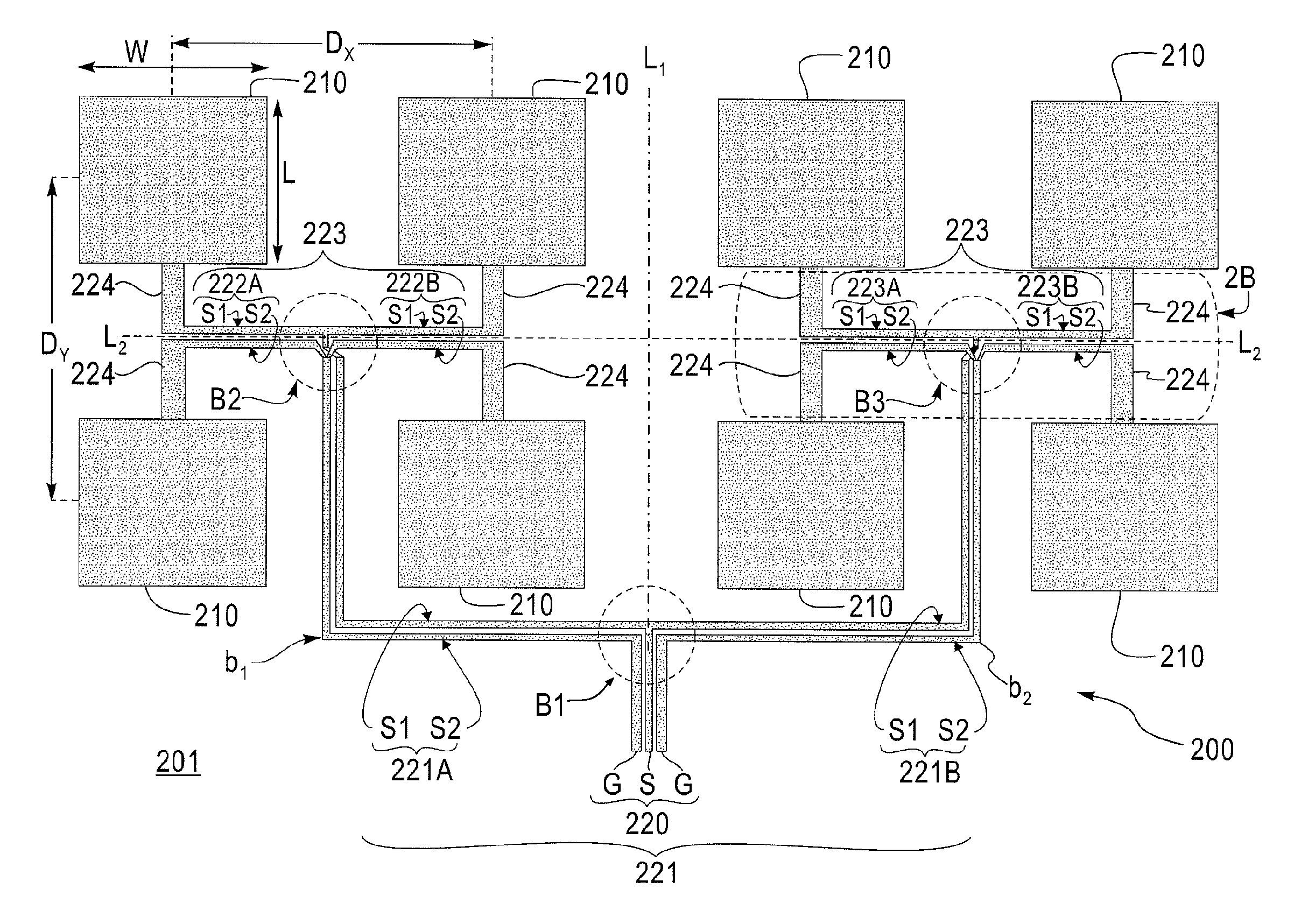
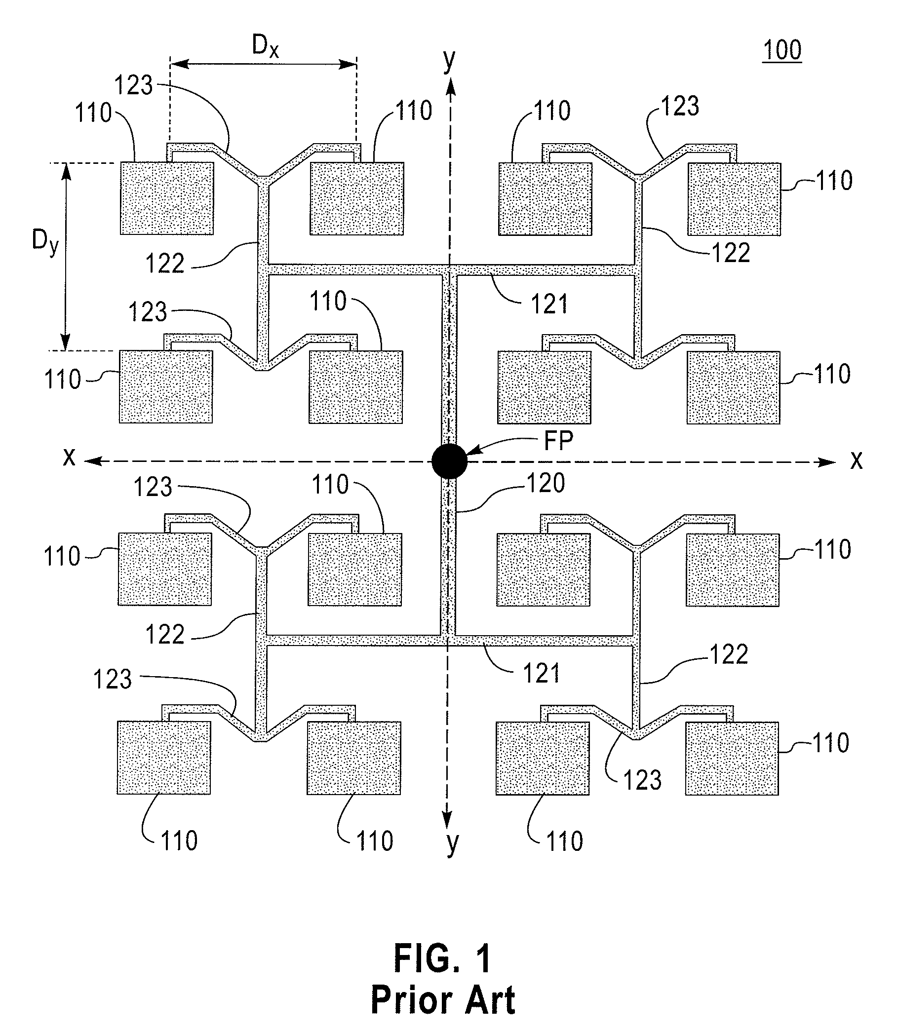
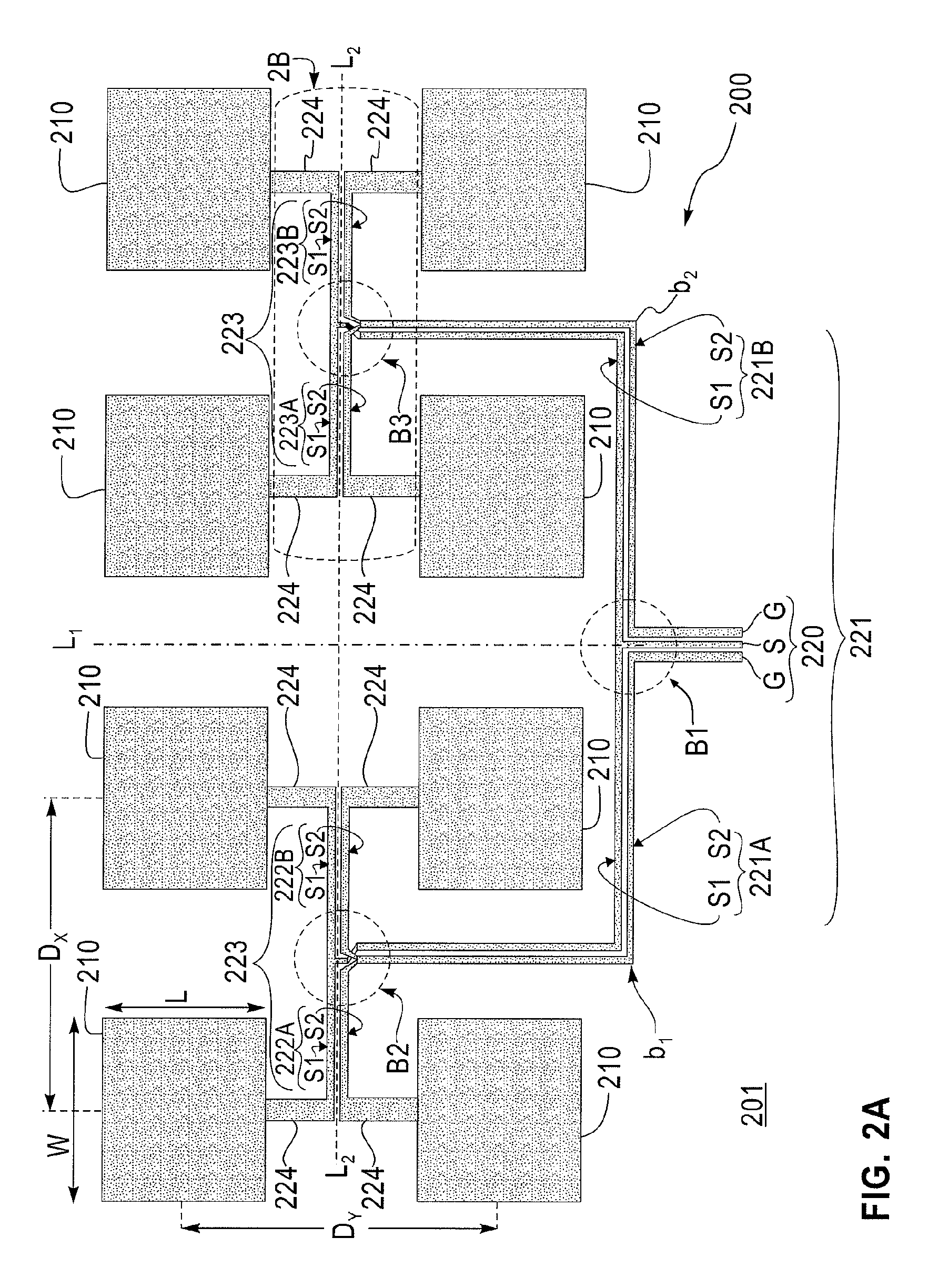
- The use of planar coplanar transmission lines, including coplanar strip lines and coplanar waveguide transmission lines interconnected with balun structures, forms a feed network that enables high-efficiency operation for millimeter wave frequencies, allowing for balanced and phased feeding of radiating elements to maximize gain and radiation efficiency.

High frequency line-to-waveguide converter and high frequency package
PatentInactiveUS7522014B2
Innovation
- A high frequency line-to-waveguide converter design featuring a coplanar line with a dielectric layer, line conductor, and ground conductor on the same surface, a slot orthogonal to the line conductor, and a shield conductor part surrounding the line and slot, along with a waveguide connected to the opposite surface, to stabilize the relative position and reduce mode coupling.


Signal Integrity Standards and Testing Methodologies
Signal integrity evaluation for microbump arrays and microstrip lines requires adherence to established industry standards that define measurement protocols, acceptable performance thresholds, and validation procedures. The primary standards governing these interconnect technologies include IEEE 802.3, JEDEC standards for high-speed digital interfaces, and IPC guidelines for advanced packaging applications. These frameworks establish baseline requirements for insertion loss, return loss, crosstalk, and impedance characteristics that must be met across different frequency ranges.
Testing methodologies for microbump arrays typically employ vector network analyzer (VNA) measurements using specialized probe stations capable of accessing densely packed interconnects. The measurement setup requires careful calibration procedures, including Short-Open-Load-Thru (SOLT) or Line-Reflect-Reflect-Match (LRRM) techniques to ensure accurate de-embedding of parasitic effects. For microbump characterization, test structures often incorporate ground-signal-ground (GSG) probe pads with pitch dimensions matching the bump array geometry.
Microstrip line evaluation follows more established protocols using coplanar waveguide test structures and standardized probe configurations. Time-domain reflectometry (TDR) and time-domain transmission (TDT) measurements complement frequency-domain analysis to provide comprehensive loss characterization. The testing frequency range typically extends from DC to several tens of gigahertz, depending on the target application bandwidth requirements.
Comparative analysis between these interconnect technologies requires normalized test conditions and consistent measurement environments. Temperature cycling, humidity exposure, and mechanical stress testing protocols ensure reliability assessment under operational conditions. Statistical analysis of measurement data across multiple samples provides confidence intervals for performance parameters and identifies process variation impacts on electrical characteristics.
Emerging test methodologies incorporate machine learning algorithms for pattern recognition in signal integrity degradation and predictive modeling of long-term performance trends. Advanced measurement techniques such as near-field scanning and electromagnetic field mapping provide detailed insight into loss mechanisms and enable optimization of interconnect designs for next-generation high-speed applications.
Testing methodologies for microbump arrays typically employ vector network analyzer (VNA) measurements using specialized probe stations capable of accessing densely packed interconnects. The measurement setup requires careful calibration procedures, including Short-Open-Load-Thru (SOLT) or Line-Reflect-Reflect-Match (LRRM) techniques to ensure accurate de-embedding of parasitic effects. For microbump characterization, test structures often incorporate ground-signal-ground (GSG) probe pads with pitch dimensions matching the bump array geometry.
Microstrip line evaluation follows more established protocols using coplanar waveguide test structures and standardized probe configurations. Time-domain reflectometry (TDR) and time-domain transmission (TDT) measurements complement frequency-domain analysis to provide comprehensive loss characterization. The testing frequency range typically extends from DC to several tens of gigahertz, depending on the target application bandwidth requirements.
Comparative analysis between these interconnect technologies requires normalized test conditions and consistent measurement environments. Temperature cycling, humidity exposure, and mechanical stress testing protocols ensure reliability assessment under operational conditions. Statistical analysis of measurement data across multiple samples provides confidence intervals for performance parameters and identifies process variation impacts on electrical characteristics.
Emerging test methodologies incorporate machine learning algorithms for pattern recognition in signal integrity degradation and predictive modeling of long-term performance trends. Advanced measurement techniques such as near-field scanning and electromagnetic field mapping provide detailed insight into loss mechanisms and enable optimization of interconnect designs for next-generation high-speed applications.
Thermal Management Considerations in Dense Interconnects
Dense interconnect architectures, particularly those utilizing microbump arrays and microstrip lines, generate significant thermal challenges that directly impact their electrical performance and reliability. The high-density packaging inherent in these systems creates localized hotspots where power dissipation becomes concentrated, leading to temperature gradients that can exceed 50°C across small areas. This thermal non-uniformity affects both the dielectric properties of substrate materials and the conductivity characteristics of metallic traces.
Microbump arrays present unique thermal management complexities due to their three-dimensional structure and limited heat dissipation pathways. The solder joints in these arrays experience thermal cycling stress, which can lead to fatigue failures and increased contact resistance over time. The small form factor of microbumps, typically ranging from 10-40 micrometers in diameter, restricts the available cross-sectional area for heat conduction, creating thermal bottlenecks that elevate junction temperatures.
Microstrip line configurations face different thermal challenges, primarily related to substrate heating and trace expansion. As temperatures rise, the dielectric constant of substrate materials changes, directly affecting the characteristic impedance and propagation delay of signal paths. FR-4 substrates commonly exhibit dielectric constant variations of 3-5% per 100°C temperature increase, while low-loss materials like Rogers laminates show more stable but still measurable thermal dependencies.
Effective thermal management strategies for dense interconnects include the implementation of thermal interface materials with high conductivity, strategic placement of thermal vias to create vertical heat conduction paths, and the use of heat spreaders or integrated heat sinks. Advanced packaging techniques such as through-silicon vias and embedded cooling channels are increasingly employed to address thermal constraints in high-performance applications.
The interaction between thermal effects and loss characteristics becomes particularly critical at higher frequencies, where skin effect losses are already elevated. Temperature-induced changes in material properties can shift the optimal operating frequency ranges and affect signal integrity parameters such as eye diagram closure and jitter performance in high-speed digital applications.
Microbump arrays present unique thermal management complexities due to their three-dimensional structure and limited heat dissipation pathways. The solder joints in these arrays experience thermal cycling stress, which can lead to fatigue failures and increased contact resistance over time. The small form factor of microbumps, typically ranging from 10-40 micrometers in diameter, restricts the available cross-sectional area for heat conduction, creating thermal bottlenecks that elevate junction temperatures.
Microstrip line configurations face different thermal challenges, primarily related to substrate heating and trace expansion. As temperatures rise, the dielectric constant of substrate materials changes, directly affecting the characteristic impedance and propagation delay of signal paths. FR-4 substrates commonly exhibit dielectric constant variations of 3-5% per 100°C temperature increase, while low-loss materials like Rogers laminates show more stable but still measurable thermal dependencies.
Effective thermal management strategies for dense interconnects include the implementation of thermal interface materials with high conductivity, strategic placement of thermal vias to create vertical heat conduction paths, and the use of heat spreaders or integrated heat sinks. Advanced packaging techniques such as through-silicon vias and embedded cooling channels are increasingly employed to address thermal constraints in high-performance applications.
The interaction between thermal effects and loss characteristics becomes particularly critical at higher frequencies, where skin effect losses are already elevated. Temperature-induced changes in material properties can shift the optimal operating frequency ranges and affect signal integrity parameters such as eye diagram closure and jitter performance in high-speed digital applications.
Unlock deeper insights with PatSnap Eureka Quick Research — get a full tech report to explore trends and direct your research. Try now!
Generate Your Research Report Instantly with AI Agent
Supercharge your innovation with PatSnap Eureka AI Agent Platform!