

Optimizing Microbump Arrays for High-Powered LEDs Use
APR 22, 20269 MIN READ
Generate Your Research Report Instantly with AI Agent
PatSnap Eureka helps you evaluate technical feasibility & market potential.
Microbump LED Technology Background and Objectives
Microbump technology represents a critical advancement in semiconductor packaging, particularly for high-powered LED applications where thermal management and electrical performance are paramount. This interconnect technology utilizes microscopic solder bumps, typically ranging from 10 to 100 micrometers in diameter, to create direct electrical connections between LED chips and substrates. The evolution of microbump arrays has been driven by the increasing demand for higher power densities, improved thermal dissipation, and enhanced reliability in LED systems.
The historical development of microbump technology traces back to the early 2000s when semiconductor manufacturers began exploring alternatives to traditional wire bonding methods. Initial applications focused on microprocessors and memory devices, but the unique requirements of high-powered LEDs presented new challenges and opportunities. The technology gained significant momentum around 2010 as LED manufacturers recognized the limitations of conventional packaging approaches in handling the thermal and electrical stresses associated with high-power operations.
Current market drivers for optimized microbump arrays in LED applications stem from several converging trends. The automotive industry's transition to LED headlights and the growing adoption of high-brightness LEDs in general lighting applications have created unprecedented demands for thermal performance. Additionally, the emergence of micro-LED displays and advanced horticultural lighting systems requires precise control over current distribution and heat dissipation at the chip level.
The primary technical objectives for optimizing microbump arrays in high-powered LED applications encompass multiple performance dimensions. Thermal management stands as the foremost priority, with the goal of achieving thermal resistance values below 1 K/W for individual LED chips. This requires careful optimization of bump pitch, diameter, and material composition to maximize heat conduction pathways while maintaining electrical integrity.
Electrical performance optimization focuses on minimizing resistance and inductance while ensuring uniform current distribution across the LED active area. Target specifications typically include contact resistance below 10 milliohms per bump and current density capabilities exceeding 10^4 A/cm². These parameters directly impact LED efficiency, color uniformity, and operational lifetime.
Reliability enhancement represents another critical objective, with industry standards demanding operational lifetimes exceeding 50,000 hours under high-power conditions. This necessitates the development of bump materials and geometries that can withstand thermal cycling, mechanical stress, and electromigration effects without degradation.
The historical development of microbump technology traces back to the early 2000s when semiconductor manufacturers began exploring alternatives to traditional wire bonding methods. Initial applications focused on microprocessors and memory devices, but the unique requirements of high-powered LEDs presented new challenges and opportunities. The technology gained significant momentum around 2010 as LED manufacturers recognized the limitations of conventional packaging approaches in handling the thermal and electrical stresses associated with high-power operations.
Current market drivers for optimized microbump arrays in LED applications stem from several converging trends. The automotive industry's transition to LED headlights and the growing adoption of high-brightness LEDs in general lighting applications have created unprecedented demands for thermal performance. Additionally, the emergence of micro-LED displays and advanced horticultural lighting systems requires precise control over current distribution and heat dissipation at the chip level.
The primary technical objectives for optimizing microbump arrays in high-powered LED applications encompass multiple performance dimensions. Thermal management stands as the foremost priority, with the goal of achieving thermal resistance values below 1 K/W for individual LED chips. This requires careful optimization of bump pitch, diameter, and material composition to maximize heat conduction pathways while maintaining electrical integrity.
Electrical performance optimization focuses on minimizing resistance and inductance while ensuring uniform current distribution across the LED active area. Target specifications typically include contact resistance below 10 milliohms per bump and current density capabilities exceeding 10^4 A/cm². These parameters directly impact LED efficiency, color uniformity, and operational lifetime.
Reliability enhancement represents another critical objective, with industry standards demanding operational lifetimes exceeding 50,000 hours under high-power conditions. This necessitates the development of bump materials and geometries that can withstand thermal cycling, mechanical stress, and electromigration effects without degradation.
Market Demand for High-Power LED Applications
The global high-power LED market has experienced unprecedented growth driven by increasing demand for energy-efficient lighting solutions across multiple sectors. Automotive lighting represents one of the most significant growth drivers, with manufacturers transitioning from traditional halogen and xenon systems to LED-based headlights, taillights, and interior lighting. The superior brightness, longevity, and design flexibility of high-power LEDs have made them essential for modern vehicle lighting architectures, particularly in premium and electric vehicle segments.
General illumination applications continue to dominate market demand, encompassing commercial, industrial, and residential lighting systems. The global shift toward smart cities and sustainable infrastructure has accelerated adoption of high-power LED street lighting, architectural lighting, and large-scale commercial installations. These applications require LEDs capable of delivering high luminous output while maintaining thermal stability and operational reliability over extended periods.
Display technology represents another rapidly expanding market segment, with high-power LEDs serving as backlighting sources for large-format displays, digital signage, and professional visualization systems. The growing demand for high-brightness outdoor displays and stadium screens has created specific requirements for LEDs with exceptional thermal management capabilities and consistent performance under varying environmental conditions.
Specialized applications in horticulture, medical devices, and industrial processing have emerged as high-growth niches. Horticultural lighting systems demand precise spectral control and high photon flux density, while medical applications require reliable, high-intensity illumination for surgical and diagnostic equipment. Industrial applications, including UV curing and materials processing, necessitate LEDs with concentrated power delivery and robust thermal characteristics.
The increasing power density requirements across these applications have intensified focus on thermal management solutions. Traditional packaging approaches face limitations in dissipating heat generated by high-current operation, leading to reduced efficiency, color shift, and shortened lifespan. This thermal challenge has created substantial market demand for advanced packaging technologies, including optimized microbump arrays that enable superior heat dissipation pathways.
Market drivers include stringent energy efficiency regulations, declining LED costs, and growing awareness of environmental sustainability. The convergence of these factors has established high-power LEDs as the preferred solution for applications requiring intense, reliable illumination, creating sustained demand for innovative thermal management approaches.
General illumination applications continue to dominate market demand, encompassing commercial, industrial, and residential lighting systems. The global shift toward smart cities and sustainable infrastructure has accelerated adoption of high-power LED street lighting, architectural lighting, and large-scale commercial installations. These applications require LEDs capable of delivering high luminous output while maintaining thermal stability and operational reliability over extended periods.
Display technology represents another rapidly expanding market segment, with high-power LEDs serving as backlighting sources for large-format displays, digital signage, and professional visualization systems. The growing demand for high-brightness outdoor displays and stadium screens has created specific requirements for LEDs with exceptional thermal management capabilities and consistent performance under varying environmental conditions.
Specialized applications in horticulture, medical devices, and industrial processing have emerged as high-growth niches. Horticultural lighting systems demand precise spectral control and high photon flux density, while medical applications require reliable, high-intensity illumination for surgical and diagnostic equipment. Industrial applications, including UV curing and materials processing, necessitate LEDs with concentrated power delivery and robust thermal characteristics.
The increasing power density requirements across these applications have intensified focus on thermal management solutions. Traditional packaging approaches face limitations in dissipating heat generated by high-current operation, leading to reduced efficiency, color shift, and shortened lifespan. This thermal challenge has created substantial market demand for advanced packaging technologies, including optimized microbump arrays that enable superior heat dissipation pathways.
Market drivers include stringent energy efficiency regulations, declining LED costs, and growing awareness of environmental sustainability. The convergence of these factors has established high-power LEDs as the preferred solution for applications requiring intense, reliable illumination, creating sustained demand for innovative thermal management approaches.
Current Microbump Array Challenges and Limitations
Microbump arrays in high-powered LED applications face significant thermal management challenges that fundamentally limit their performance and reliability. The primary constraint stems from the inherently high current densities required for high-power operation, which generate substantial heat flux through the microscopic interconnection points. Current microbump designs typically exhibit thermal resistance values ranging from 10-50 K/W per bump, creating localized hotspots that can exceed 150°C during peak operation.
Mechanical reliability represents another critical limitation in existing microbump array implementations. The coefficient of thermal expansion mismatch between LED chip materials and substrate materials creates cyclic stress concentrations at bump interfaces during thermal cycling. This phenomenon leads to fatigue crack propagation and eventual interconnection failure, with typical failure rates increasing exponentially after 1000-3000 thermal cycles in high-power applications.
Current density distribution across microbump arrays suffers from inherent non-uniformity issues that compromise LED performance. Conventional bump layouts often result in current crowding effects near array peripheries, leading to uneven light output and accelerated degradation of specific LED segments. The typical current density variation can reach 20-30% across the array, significantly impacting overall luminous efficacy and color uniformity.
Manufacturing precision limitations pose substantial challenges for achieving optimal microbump array performance. Current lithographic and assembly processes struggle to maintain consistent bump height variations within ±2 micrometers across large arrays, resulting in uneven electrical contact resistance. This variation directly translates to non-uniform current distribution and localized heating effects that degrade overall system performance.
Electrical parasitic effects in existing microbump configurations create additional performance bottlenecks. The small cross-sectional area of individual bumps, combined with their relatively high aspect ratios, introduces significant series resistance and inductance that becomes problematic at high switching frequencies. These parasitic effects limit the dynamic response of LED systems and contribute to power conversion inefficiencies.
Material degradation mechanisms present long-term reliability concerns for current microbump array technologies. Electromigration effects become pronounced under high current densities, causing gradual material redistribution within bump structures. Additionally, intermetallic compound formation at bump interfaces can increase contact resistance over time, leading to progressive performance degradation and eventual system failure.
Mechanical reliability represents another critical limitation in existing microbump array implementations. The coefficient of thermal expansion mismatch between LED chip materials and substrate materials creates cyclic stress concentrations at bump interfaces during thermal cycling. This phenomenon leads to fatigue crack propagation and eventual interconnection failure, with typical failure rates increasing exponentially after 1000-3000 thermal cycles in high-power applications.
Current density distribution across microbump arrays suffers from inherent non-uniformity issues that compromise LED performance. Conventional bump layouts often result in current crowding effects near array peripheries, leading to uneven light output and accelerated degradation of specific LED segments. The typical current density variation can reach 20-30% across the array, significantly impacting overall luminous efficacy and color uniformity.
Manufacturing precision limitations pose substantial challenges for achieving optimal microbump array performance. Current lithographic and assembly processes struggle to maintain consistent bump height variations within ±2 micrometers across large arrays, resulting in uneven electrical contact resistance. This variation directly translates to non-uniform current distribution and localized heating effects that degrade overall system performance.
Electrical parasitic effects in existing microbump configurations create additional performance bottlenecks. The small cross-sectional area of individual bumps, combined with their relatively high aspect ratios, introduces significant series resistance and inductance that becomes problematic at high switching frequencies. These parasitic effects limit the dynamic response of LED systems and contribute to power conversion inefficiencies.
Material degradation mechanisms present long-term reliability concerns for current microbump array technologies. Electromigration effects become pronounced under high current densities, causing gradual material redistribution within bump structures. Additionally, intermetallic compound formation at bump interfaces can increase contact resistance over time, leading to progressive performance degradation and eventual system failure.
Existing Microbump Optimization Solutions
01 Formation methods for microbump arrays using electroplating and deposition techniques
Microbump arrays can be formed through various electroplating and deposition methods to create reliable interconnection structures. These techniques involve depositing conductive materials onto substrates with controlled dimensions and spacing. The formation process typically includes photolithography, seed layer deposition, and selective plating to achieve uniform microbump heights and shapes. Advanced deposition methods enable precise control over bump geometry and material composition for improved electrical and mechanical performance.- Formation methods for microbump arrays using electroplating and deposition techniques: Microbump arrays can be formed through various electroplating and deposition methods to create reliable interconnection structures. These techniques involve depositing conductive materials onto substrates with controlled dimensions and spacing. The formation process typically includes photolithography patterning, seed layer deposition, and selective material growth to achieve uniform microbump structures with precise height and pitch control.
- Underfill and encapsulation materials for microbump array protection: Protection of microbump arrays requires specialized underfill and encapsulation materials to ensure mechanical stability and electrical reliability. These materials fill the gaps between bumps and provide stress relief during thermal cycling. The encapsulation process involves dispensing flowable materials that cure to form protective layers, preventing moisture ingress and mechanical damage while maintaining electrical performance.
- Fine pitch microbump structures for high-density interconnections: Advanced microbump arrays feature fine pitch designs to enable high-density interconnections in semiconductor packaging. These structures utilize reduced bump dimensions and spacing to increase input/output density. Manufacturing processes for fine pitch microbumps require precise alignment capabilities and advanced lithography techniques to achieve pitches below 40 micrometers while maintaining yield and reliability.
- Copper pillar microbump technology for enhanced electrical performance: Copper pillar microbumps provide superior electrical and thermal performance compared to traditional solder bumps. These structures consist of copper columns with solder caps, offering lower resistance and better current carrying capacity. The fabrication involves copper electroplating to form pillars followed by solder deposition, enabling improved signal integrity and power delivery in advanced packaging applications.
- Testing and inspection methods for microbump array quality control: Quality control of microbump arrays requires specialized testing and inspection methodologies to ensure manufacturing reliability. These methods include optical inspection, X-ray imaging, and electrical testing to detect defects such as voids, misalignment, or incomplete connections. Advanced inspection systems utilize automated image analysis and probe testing to verify bump height uniformity, coplanarity, and electrical continuity across the entire array.
02 Structural configurations and pitch designs for high-density microbump arrays
High-density microbump arrays require optimized structural configurations to achieve fine pitch interconnections. The design considerations include bump diameter, height, pitch spacing, and array layout patterns to maximize connection density while maintaining reliability. Various geometrical arrangements and pitch reduction techniques enable increased input/output density for advanced packaging applications. The structural design also addresses stress distribution and thermal management in densely packed arrays.Expand Specific Solutions03 Underfill and encapsulation materials for microbump array protection
Underfill materials and encapsulation techniques are essential for protecting microbump arrays from mechanical stress and environmental factors. These materials fill the gaps between bonded surfaces to enhance mechanical strength and reliability. The encapsulation process involves dispensing flowable materials that cure to form protective layers around the microbump structures. Proper underfill selection and application methods improve thermal cycling performance and prevent crack propagation in the interconnection region.Expand Specific Solutions04 Bonding and assembly processes for microbump array interconnections
Bonding processes for microbump arrays involve thermocompression, mass reflow, or hybrid bonding techniques to establish electrical and mechanical connections. The assembly process requires precise alignment and controlled temperature and pressure conditions to achieve reliable joints. Various bonding methods address different material combinations and thermal budget constraints. Process optimization focuses on minimizing voids, achieving uniform bond line thickness, and ensuring high yield in mass production environments.Expand Specific Solutions05 Testing and inspection methods for microbump array quality control
Quality control of microbump arrays requires specialized testing and inspection techniques to verify dimensional accuracy and electrical connectivity. Non-destructive inspection methods include optical imaging, X-ray inspection, and acoustic microscopy to detect defects such as voids, misalignment, or incomplete bonding. Electrical testing validates the continuity and resistance of individual connections within the array. Advanced metrology tools enable high-throughput inspection of bump height uniformity, coplanarity, and positional accuracy to ensure manufacturing quality standards are met.Expand Specific Solutions
Key Players in LED and Microbump Industries
The microbump array optimization for high-powered LEDs represents a rapidly evolving market segment within the broader LED industry, which has transitioned from growth to maturity phase with increasing focus on specialized applications. The global LED market, valued at approximately $75 billion, continues expanding driven by automotive, display, and general lighting applications. Technology maturity varies significantly across market players, with established giants like Lumileds LLC, Koninklijke Philips NV, and OSRAM SYLVANIA leading in traditional LED packaging, while companies such as VueReal Inc. and Jade Bird Display pioneer advanced microLED technologies. Asian manufacturers including EPISTAR Corp., BOE Technology Group, and Wolfspeed Inc. demonstrate strong capabilities in semiconductor materials and manufacturing processes. The competitive landscape shows a clear division between mature thermal management solutions from traditional players and emerging innovative approaches from specialized firms targeting next-generation high-power applications.
Lumileds LLC
Technical Solution: Lumileds has developed advanced microbump array technologies specifically for high-power LED applications, focusing on copper-based microbump structures with optimized pitch spacing of 20-50 micrometers. Their approach utilizes electroplating techniques to create uniform bump heights with tight tolerances of ±2 micrometers, ensuring reliable electrical and thermal connections. The company has implemented advanced underfill materials with low coefficient of thermal expansion to minimize stress during thermal cycling. Their microbump arrays feature enhanced current spreading capabilities through optimized metallization layers, enabling current densities up to 100 A/cm² while maintaining junction temperatures below 85°C for extended operational lifetime.
Strengths: Industry-leading thermal management and current handling capabilities, proven reliability in automotive applications. Weaknesses: Higher manufacturing costs compared to traditional wire bonding, limited scalability for ultra-fine pitch applications.
Creeled Inc
Technical Solution: Creeled has pioneered silicon carbide substrate-based LED packages with innovative microbump array designs optimized for high-power applications exceeding 10W per device. Their technology employs gold-tin eutectic microbumps with diameters ranging from 25-40 micrometers, arranged in hexagonal patterns to maximize current distribution uniformity. The company's approach integrates advanced thermal interface materials between microbumps to achieve thermal resistance values below 1 K/W. Their proprietary bump formation process utilizes photolithography and selective electroplating to achieve aspect ratios of 1:1.5, enabling robust mechanical connections while minimizing electrical resistance to less than 10 milliohms per bump.
Strengths: Excellent thermal performance with SiC substrates, superior current uniformity distribution. Weaknesses: Limited to specific substrate materials, higher material costs due to gold content.
Core Innovations in Microbump Array Design
Method for fabricating high-power light-emitting diode arrays
PatentActiveUS20100176404A1
Innovation
- A method involving etching grooves on a growth substrate to form mesas, fabricating indium gallium aluminum nitride (InGaAlN) multilayer structures, bonding these structures to a conductive substrate, removing the growth substrate, and creating conductive paths to couple adjacent LEDs for a common power supply, forming high-power LED arrays without reducing yield rates.


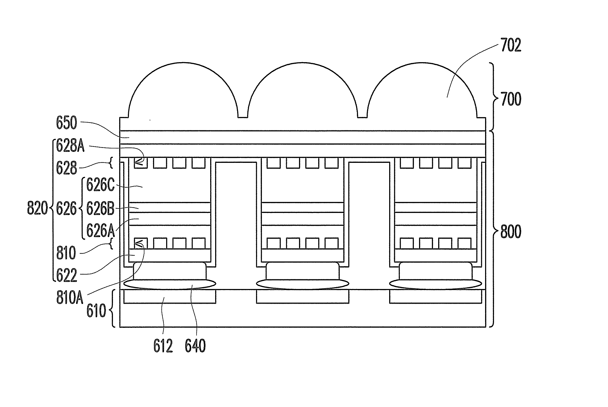
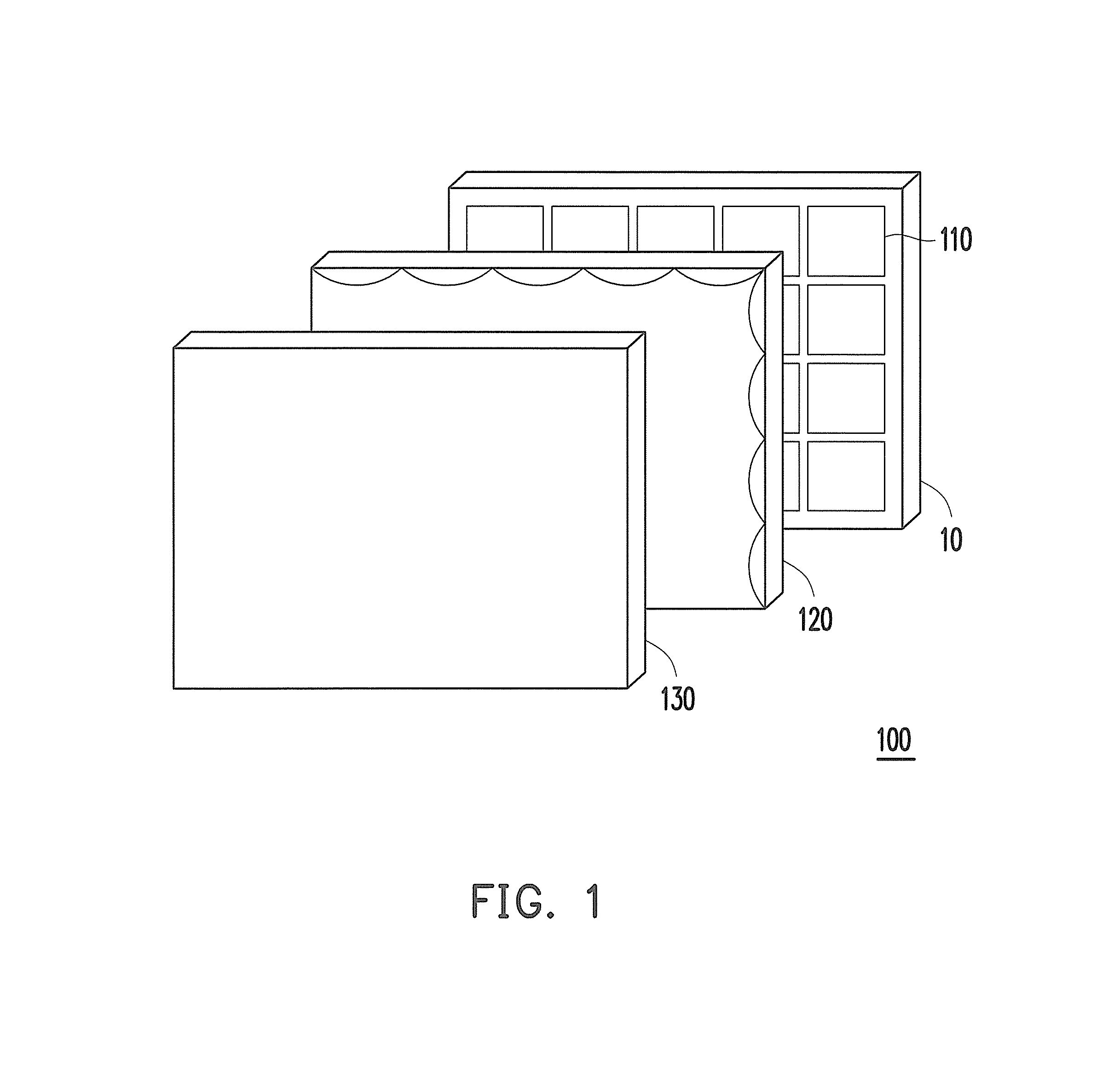
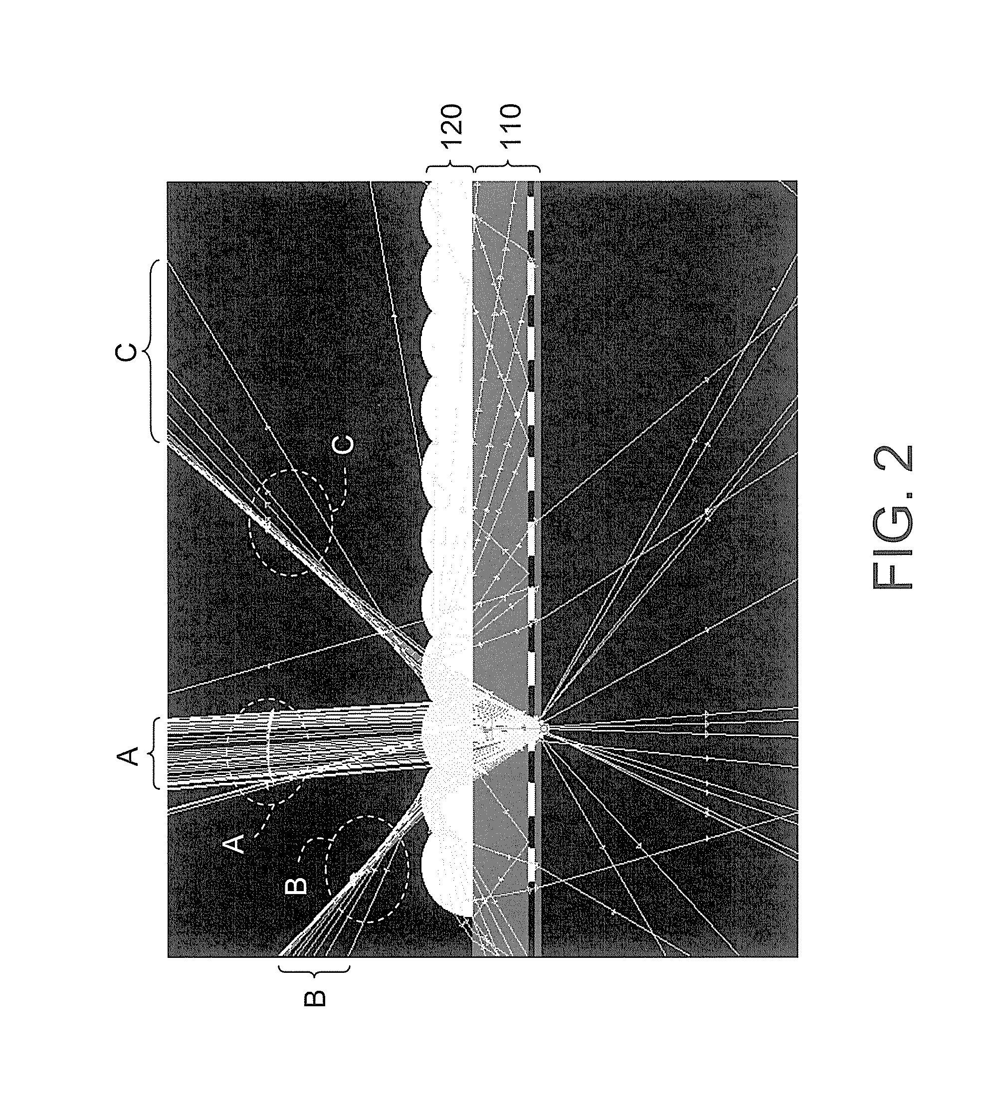
Light emitting unit array and projection system
PatentActiveUS20120050694A1
Innovation
- A micro-projection system utilizing a micro-light emitting diode (μ-LED) array as the imaging source, which includes a reflection layer, light emitting structure, and light collimation structure, such as a photonic crystal layer, to improve light collimation and reduce volume, eliminating the need for a complex optical engine.

Thermal Management Standards for High-Power LEDs
The thermal management of high-power LEDs requires adherence to stringent standards that ensure optimal performance, longevity, and safety. Current industry standards primarily focus on junction temperature limits, typically maintaining LED junction temperatures below 125°C for standard applications and 150°C for specialized high-temperature variants. These thresholds are critical for preserving luminous efficacy and preventing accelerated degradation of semiconductor materials.
International standards organizations, including IES (Illuminating Engineering Society) and CIE (International Commission on Illumination), have established comprehensive guidelines for LED thermal characterization. The JEDEC JESD51 series provides standardized methodologies for measuring thermal resistance from junction to ambient, while IES LM-85 specifically addresses thermal testing procedures for LED packages and arrays.
For microbump array applications in high-power LEDs, thermal interface material (TIM) standards become particularly relevant. ASTM D5470 defines the standard test method for thermal transmission properties of thermally conductive electrical insulation materials, establishing benchmarks for thermal conductivity measurements that directly impact microbump design optimization.
Package-level thermal standards emphasize the importance of thermal resistance values, typically requiring Rth-ja (junction-to-ambient thermal resistance) below 10 K/W for high-power applications. Advanced packaging standards also specify requirements for thermal cycling reliability, with IPC-9701A providing guidelines for board-level drop test and thermal cycling performance that directly influence microbump array durability.
Emerging standards address multi-chip LED modules and array configurations, recognizing the unique thermal challenges posed by densely packed LED arrangements. These standards incorporate thermal spreading considerations, emphasizing the need for effective heat distribution mechanisms that microbump arrays can facilitate through optimized pitch spacing and material selection.
Safety standards such as UL 8750 and IEC 62031 establish maximum case temperature limits and thermal protection requirements, ensuring that LED systems operate within safe thermal boundaries while maintaining performance specifications throughout their operational lifetime.
International standards organizations, including IES (Illuminating Engineering Society) and CIE (International Commission on Illumination), have established comprehensive guidelines for LED thermal characterization. The JEDEC JESD51 series provides standardized methodologies for measuring thermal resistance from junction to ambient, while IES LM-85 specifically addresses thermal testing procedures for LED packages and arrays.
For microbump array applications in high-power LEDs, thermal interface material (TIM) standards become particularly relevant. ASTM D5470 defines the standard test method for thermal transmission properties of thermally conductive electrical insulation materials, establishing benchmarks for thermal conductivity measurements that directly impact microbump design optimization.
Package-level thermal standards emphasize the importance of thermal resistance values, typically requiring Rth-ja (junction-to-ambient thermal resistance) below 10 K/W for high-power applications. Advanced packaging standards also specify requirements for thermal cycling reliability, with IPC-9701A providing guidelines for board-level drop test and thermal cycling performance that directly influence microbump array durability.
Emerging standards address multi-chip LED modules and array configurations, recognizing the unique thermal challenges posed by densely packed LED arrangements. These standards incorporate thermal spreading considerations, emphasizing the need for effective heat distribution mechanisms that microbump arrays can facilitate through optimized pitch spacing and material selection.
Safety standards such as UL 8750 and IEC 62031 establish maximum case temperature limits and thermal protection requirements, ensuring that LED systems operate within safe thermal boundaries while maintaining performance specifications throughout their operational lifetime.
Reliability Testing Methods for Microbump Arrays
Reliability testing for microbump arrays in high-powered LED applications requires comprehensive methodologies that address the unique thermal, mechanical, and electrical stresses these interconnects experience. The testing protocols must simulate real-world operating conditions while accelerating failure mechanisms to predict long-term performance within reasonable timeframes.
Thermal cycling testing represents the primary reliability assessment method, subjecting microbump arrays to repeated temperature excursions between -40°C and 150°C. This testing evaluates the coefficient of thermal expansion mismatch between different materials in the LED package, particularly between the LED die, microbumps, and substrate materials. The cycling frequency typically ranges from 15 to 60 minutes per cycle, with failure criteria defined as a 20% increase in electrical resistance or complete open circuit formation.
Power cycling tests complement thermal cycling by applying electrical stress while monitoring junction temperature rise. These tests operate LEDs at rated current levels for defined on-off periods, typically 10 seconds on and 10 seconds off, while measuring forward voltage degradation and thermal resistance changes. The combination of electrical and thermal stress provides insights into electromigration effects and thermomechanical fatigue specific to operational conditions.
Mechanical shock and vibration testing evaluates microbump integrity under physical stress conditions. Standard protocols include drop tests following JEDEC JESD22-B111 specifications and vibration testing per MIL-STD-883 requirements. These tests assess the mechanical robustness of the microbump connections and identify potential failure modes related to solder joint cracking or delamination at interfaces.
Highly accelerated life testing utilizes elevated temperature and humidity conditions, typically 85°C/85% relative humidity, to accelerate corrosion and moisture-related degradation mechanisms. This testing is particularly relevant for microbump arrays using copper or other oxidation-prone materials, as it reveals long-term reliability issues related to intermetallic compound formation and corrosion.
Advanced characterization techniques support these testing methods, including cross-sectional analysis using scanning electron microscopy, X-ray computed tomography for non-destructive void detection, and thermal imaging for hot spot identification. Real-time monitoring capabilities enable continuous assessment of electrical parameters, thermal performance, and optical output degradation throughout testing periods.
Thermal cycling testing represents the primary reliability assessment method, subjecting microbump arrays to repeated temperature excursions between -40°C and 150°C. This testing evaluates the coefficient of thermal expansion mismatch between different materials in the LED package, particularly between the LED die, microbumps, and substrate materials. The cycling frequency typically ranges from 15 to 60 minutes per cycle, with failure criteria defined as a 20% increase in electrical resistance or complete open circuit formation.
Power cycling tests complement thermal cycling by applying electrical stress while monitoring junction temperature rise. These tests operate LEDs at rated current levels for defined on-off periods, typically 10 seconds on and 10 seconds off, while measuring forward voltage degradation and thermal resistance changes. The combination of electrical and thermal stress provides insights into electromigration effects and thermomechanical fatigue specific to operational conditions.
Mechanical shock and vibration testing evaluates microbump integrity under physical stress conditions. Standard protocols include drop tests following JEDEC JESD22-B111 specifications and vibration testing per MIL-STD-883 requirements. These tests assess the mechanical robustness of the microbump connections and identify potential failure modes related to solder joint cracking or delamination at interfaces.
Highly accelerated life testing utilizes elevated temperature and humidity conditions, typically 85°C/85% relative humidity, to accelerate corrosion and moisture-related degradation mechanisms. This testing is particularly relevant for microbump arrays using copper or other oxidation-prone materials, as it reveals long-term reliability issues related to intermetallic compound formation and corrosion.
Advanced characterization techniques support these testing methods, including cross-sectional analysis using scanning electron microscopy, X-ray computed tomography for non-destructive void detection, and thermal imaging for hot spot identification. Real-time monitoring capabilities enable continuous assessment of electrical parameters, thermal performance, and optical output degradation throughout testing periods.
Unlock deeper insights with PatSnap Eureka Quick Research — get a full tech report to explore trends and direct your research. Try now!
Generate Your Research Report Instantly with AI Agent
Supercharge your innovation with PatSnap Eureka AI Agent Platform!