

Microbump Arrays vs Rigid-Flex PCBs: Development Cost
APR 22, 202610 MIN READ
Generate Your Research Report Instantly with AI Agent
PatSnap Eureka helps you evaluate technical feasibility & market potential.
Microbump and Rigid-Flex PCB Technology Background and Goals
The evolution of electronic packaging technologies has been driven by the relentless pursuit of miniaturization, enhanced performance, and cost optimization in modern electronic systems. Two critical interconnection technologies have emerged as pivotal solutions for advanced packaging applications: microbump arrays and rigid-flex printed circuit boards (PCBs). These technologies represent distinct approaches to addressing the fundamental challenges of electrical connectivity, mechanical reliability, and thermal management in increasingly complex electronic assemblies.
Microbump technology originated from the semiconductor industry's need for high-density interconnections in advanced packaging applications. This technology enables direct chip-to-substrate connections through microscopic solder bumps, typically ranging from 10 to 100 micrometers in diameter. The development trajectory of microbumps has been closely aligned with the progression of Moore's Law, facilitating the transition from wire bonding to area array connections that support higher I/O densities and improved electrical performance.
Rigid-flex PCB technology emerged as a hybrid solution combining the mechanical flexibility of flexible circuits with the structural integrity of rigid boards. This technology addresses the spatial constraints and reliability requirements of modern electronic devices by eliminating traditional connectors and enabling three-dimensional packaging configurations. The evolution of rigid-flex technology has been particularly influenced by the miniaturization demands of portable electronics and aerospace applications.
The primary technical objectives driving the development of both technologies center on achieving optimal balance between performance, reliability, and manufacturing cost. For microbump arrays, key goals include minimizing interconnection pitch while maintaining acceptable yield rates, enhancing thermal and electrical performance through reduced parasitic effects, and developing scalable manufacturing processes that support volume production economics.
Rigid-flex PCB development focuses on optimizing the transition zones between rigid and flexible sections to ensure mechanical durability, advancing materials science to support higher frequency applications, and streamlining manufacturing processes to reduce the inherent complexity and associated costs. Both technologies aim to address the growing demand for compact, high-performance electronic systems while maintaining economic viability in competitive markets.
The convergence of these technologies reflects the industry's recognition that future electronic packaging solutions must simultaneously address multiple performance vectors while remaining economically sustainable for large-scale deployment across diverse application domains.
Microbump technology originated from the semiconductor industry's need for high-density interconnections in advanced packaging applications. This technology enables direct chip-to-substrate connections through microscopic solder bumps, typically ranging from 10 to 100 micrometers in diameter. The development trajectory of microbumps has been closely aligned with the progression of Moore's Law, facilitating the transition from wire bonding to area array connections that support higher I/O densities and improved electrical performance.
Rigid-flex PCB technology emerged as a hybrid solution combining the mechanical flexibility of flexible circuits with the structural integrity of rigid boards. This technology addresses the spatial constraints and reliability requirements of modern electronic devices by eliminating traditional connectors and enabling three-dimensional packaging configurations. The evolution of rigid-flex technology has been particularly influenced by the miniaturization demands of portable electronics and aerospace applications.
The primary technical objectives driving the development of both technologies center on achieving optimal balance between performance, reliability, and manufacturing cost. For microbump arrays, key goals include minimizing interconnection pitch while maintaining acceptable yield rates, enhancing thermal and electrical performance through reduced parasitic effects, and developing scalable manufacturing processes that support volume production economics.
Rigid-flex PCB development focuses on optimizing the transition zones between rigid and flexible sections to ensure mechanical durability, advancing materials science to support higher frequency applications, and streamlining manufacturing processes to reduce the inherent complexity and associated costs. Both technologies aim to address the growing demand for compact, high-performance electronic systems while maintaining economic viability in competitive markets.
The convergence of these technologies reflects the industry's recognition that future electronic packaging solutions must simultaneously address multiple performance vectors while remaining economically sustainable for large-scale deployment across diverse application domains.
Market Demand Analysis for Advanced PCB Interconnect Solutions
The global electronics industry is experiencing unprecedented demand for advanced PCB interconnect solutions, driven by the relentless miniaturization of electronic devices and the exponential growth in data processing requirements. Consumer electronics, automotive systems, and telecommunications infrastructure are pushing the boundaries of traditional interconnect technologies, creating substantial market opportunities for both microbump arrays and rigid-flex PCB solutions.
Mobile device manufacturers represent the largest segment driving demand for advanced interconnect solutions. Smartphones, tablets, and wearable devices require increasingly compact form factors while maintaining high-performance connectivity between processors, memory modules, and peripheral components. The transition to 5G networks has intensified these requirements, as devices must accommodate additional RF components and higher-frequency signal processing capabilities within constrained spaces.
The automotive sector presents another significant growth driver, particularly with the accelerating adoption of electric vehicles and autonomous driving technologies. Modern vehicles integrate numerous electronic control units, advanced driver assistance systems, and infotainment platforms that demand reliable, high-density interconnect solutions capable of withstanding harsh environmental conditions. The shift toward centralized computing architectures in vehicles further amplifies the need for sophisticated PCB interconnect technologies.
Data center and cloud computing infrastructure constitute a rapidly expanding market segment for advanced interconnect solutions. The proliferation of artificial intelligence applications, machine learning workloads, and edge computing deployments requires high-performance computing systems with exceptional signal integrity and thermal management capabilities. These applications often justify premium interconnect solutions due to their critical performance requirements and revenue generation potential.
Industrial automation and Internet of Things applications are creating diverse demand patterns across multiple vertical markets. Manufacturing equipment, medical devices, and aerospace systems increasingly require compact, reliable interconnect solutions that can operate in challenging environments while maintaining long-term reliability. These applications often prioritize durability and performance over cost considerations.
Market dynamics reveal distinct preferences between microbump arrays and rigid-flex PCBs across different application segments. High-volume consumer electronics applications typically favor solutions that can achieve cost optimization through manufacturing scale, while specialized industrial and aerospace applications prioritize performance and reliability characteristics. The development cost considerations significantly influence technology adoption patterns, particularly for companies with limited R&D budgets or shorter product development cycles.
Mobile device manufacturers represent the largest segment driving demand for advanced interconnect solutions. Smartphones, tablets, and wearable devices require increasingly compact form factors while maintaining high-performance connectivity between processors, memory modules, and peripheral components. The transition to 5G networks has intensified these requirements, as devices must accommodate additional RF components and higher-frequency signal processing capabilities within constrained spaces.
The automotive sector presents another significant growth driver, particularly with the accelerating adoption of electric vehicles and autonomous driving technologies. Modern vehicles integrate numerous electronic control units, advanced driver assistance systems, and infotainment platforms that demand reliable, high-density interconnect solutions capable of withstanding harsh environmental conditions. The shift toward centralized computing architectures in vehicles further amplifies the need for sophisticated PCB interconnect technologies.
Data center and cloud computing infrastructure constitute a rapidly expanding market segment for advanced interconnect solutions. The proliferation of artificial intelligence applications, machine learning workloads, and edge computing deployments requires high-performance computing systems with exceptional signal integrity and thermal management capabilities. These applications often justify premium interconnect solutions due to their critical performance requirements and revenue generation potential.
Industrial automation and Internet of Things applications are creating diverse demand patterns across multiple vertical markets. Manufacturing equipment, medical devices, and aerospace systems increasingly require compact, reliable interconnect solutions that can operate in challenging environments while maintaining long-term reliability. These applications often prioritize durability and performance over cost considerations.
Market dynamics reveal distinct preferences between microbump arrays and rigid-flex PCBs across different application segments. High-volume consumer electronics applications typically favor solutions that can achieve cost optimization through manufacturing scale, while specialized industrial and aerospace applications prioritize performance and reliability characteristics. The development cost considerations significantly influence technology adoption patterns, particularly for companies with limited R&D budgets or shorter product development cycles.
Current State and Cost Challenges in Microbump vs Rigid-Flex
The current landscape of advanced packaging technologies presents a complex cost-benefit analysis between microbump arrays and rigid-flex PCBs, each representing distinct approaches to high-density interconnection challenges. Microbump technology, primarily utilized in advanced semiconductor packaging applications such as 2.5D and 3D integrated circuits, faces significant manufacturing cost pressures due to its reliance on sophisticated lithography processes and precision placement equipment. The technology requires specialized facilities with cleanroom environments, advanced bumping tools, and high-precision alignment systems, resulting in substantial capital expenditure requirements.
Manufacturing costs for microbump arrays are heavily influenced by pitch requirements, with finer pitches below 40 micrometers demanding more expensive processing equipment and yielding lower production throughput. Current industry data indicates that microbump processing costs range from $15-50 per square centimeter depending on pitch density and substrate complexity. The technology also faces yield challenges, particularly in mass transfer processes and thermal compression bonding, which can significantly impact overall cost-effectiveness.
Rigid-flex PCB technology, while more mature, encounters its own cost challenges primarily related to material expenses and manufacturing complexity. The integration of flexible polyimide sections with rigid FR-4 substrates requires specialized lamination processes and precise registration control. Material costs for high-performance flexible substrates can be 3-5 times higher than standard rigid PCB materials, with additional expenses arising from specialized drilling, plating, and assembly processes.
The rigid-flex manufacturing process involves multiple lamination cycles and complex tooling requirements, contributing to extended production lead times and higher labor costs. Current market pricing for rigid-flex solutions ranges from $200-800 per square meter, depending on layer count, via density, and flexibility requirements. Design rule constraints and the need for specialized design software further increase development overhead costs.
Both technologies face scalability challenges that directly impact cost structures. Microbump arrays struggle with throughput limitations in current manufacturing equipment, while rigid-flex PCBs encounter yield issues related to stress concentration at rigid-flex transition zones. Supply chain constraints for specialized materials and equipment create additional cost volatility, particularly affecting smaller volume applications where economies of scale cannot be achieved.
The cost comparison becomes more complex when considering total system costs, including assembly, testing, and reliability requirements. Microbump solutions often require additional underfill processes and specialized inspection equipment, while rigid-flex designs may necessitate custom assembly fixtures and modified testing protocols. These factors contribute to the overall development cost equation that organizations must carefully evaluate when selecting between these competing technologies.
Manufacturing costs for microbump arrays are heavily influenced by pitch requirements, with finer pitches below 40 micrometers demanding more expensive processing equipment and yielding lower production throughput. Current industry data indicates that microbump processing costs range from $15-50 per square centimeter depending on pitch density and substrate complexity. The technology also faces yield challenges, particularly in mass transfer processes and thermal compression bonding, which can significantly impact overall cost-effectiveness.
Rigid-flex PCB technology, while more mature, encounters its own cost challenges primarily related to material expenses and manufacturing complexity. The integration of flexible polyimide sections with rigid FR-4 substrates requires specialized lamination processes and precise registration control. Material costs for high-performance flexible substrates can be 3-5 times higher than standard rigid PCB materials, with additional expenses arising from specialized drilling, plating, and assembly processes.
The rigid-flex manufacturing process involves multiple lamination cycles and complex tooling requirements, contributing to extended production lead times and higher labor costs. Current market pricing for rigid-flex solutions ranges from $200-800 per square meter, depending on layer count, via density, and flexibility requirements. Design rule constraints and the need for specialized design software further increase development overhead costs.
Both technologies face scalability challenges that directly impact cost structures. Microbump arrays struggle with throughput limitations in current manufacturing equipment, while rigid-flex PCBs encounter yield issues related to stress concentration at rigid-flex transition zones. Supply chain constraints for specialized materials and equipment create additional cost volatility, particularly affecting smaller volume applications where economies of scale cannot be achieved.
The cost comparison becomes more complex when considering total system costs, including assembly, testing, and reliability requirements. Microbump solutions often require additional underfill processes and specialized inspection equipment, while rigid-flex designs may necessitate custom assembly fixtures and modified testing protocols. These factors contribute to the overall development cost equation that organizations must carefully evaluate when selecting between these competing technologies.
Current Cost-Effective Solutions for PCB Interconnects
01 Microbump array structure and manufacturing methods
Microbump arrays utilize advanced interconnection structures with fine-pitch bumps for chip-to-chip or chip-to-substrate connections. Manufacturing methods include photolithography, electroplating, and reflow processes to form uniform microbump arrays. These structures enable high-density interconnections with reduced footprint, which can lower material costs and improve manufacturing efficiency compared to traditional interconnection methods.- Microbump array fabrication methods and cost reduction techniques: Various fabrication methods for microbump arrays focus on reducing manufacturing costs through simplified processes, including photolithography-free approaches, single-step formation techniques, and optimized material deposition methods. These techniques aim to minimize the number of processing steps, reduce material waste, and improve yield rates, thereby lowering overall development and production costs compared to traditional methods.
- Rigid-flex PCB manufacturing process optimization: Manufacturing processes for rigid-flex PCBs incorporate cost-effective techniques such as integrated drilling methods, simplified layer stacking procedures, and automated alignment systems. These innovations reduce labor costs, minimize material usage, and decrease production time. The development focuses on streamlining the transition between rigid and flexible sections while maintaining reliability and reducing defect rates.
- Interconnection structure design for cost efficiency: Design approaches for interconnection structures emphasize cost reduction through optimized bump pitch configurations, reduced layer counts, and simplified via structures. These designs balance electrical performance requirements with manufacturing complexity, enabling lower tooling costs and faster production cycles. The structures accommodate both microbump and rigid-flex applications with adaptable architectures.
- Testing and reliability assessment methodologies: Cost-effective testing methodologies for both microbump arrays and rigid-flex PCBs include accelerated reliability testing protocols, automated inspection systems, and predictive failure analysis techniques. These approaches reduce development costs by identifying potential issues early in the design phase, minimizing expensive redesigns and improving time-to-market while ensuring product quality and longevity.
- Hybrid packaging solutions and integration strategies: Hybrid packaging approaches combine elements of microbump technology and rigid-flex PCB designs to optimize cost-performance ratios. These solutions leverage the advantages of each technology, implementing selective use of advanced interconnection methods only where necessary while using conventional techniques elsewhere. This strategic integration reduces overall development costs while maintaining required functionality and reliability standards.
02 Rigid-flex PCB design and fabrication processes
Rigid-flex printed circuit boards combine rigid and flexible substrates to create three-dimensional interconnection solutions. The fabrication process involves multiple lamination steps, drilling, and selective etching to form both rigid and flexible regions. Development costs are influenced by the complexity of layer stackup, material selection, and the need for specialized manufacturing equipment and processes.Expand Specific Solutions03 Cost reduction through simplified interconnection structures
Simplified interconnection architectures reduce development costs by minimizing the number of processing steps and material layers required. Techniques include optimized via structures, reduced layer counts, and streamlined assembly processes. These approaches can significantly decrease both tooling costs and production time, making them economically advantageous for high-volume manufacturing.Expand Specific Solutions04 Advanced packaging integration for cost optimization
Advanced packaging technologies integrate multiple functions into compact assemblies, reducing overall system costs. Methods include wafer-level packaging, system-in-package configurations, and heterogeneous integration approaches. These technologies can eliminate the need for complex rigid-flex designs in certain applications, offering alternative cost-effective solutions with comparable performance.Expand Specific Solutions05 Testing and reliability considerations affecting development costs
Testing methodologies and reliability requirements significantly impact development costs for both microbump arrays and rigid-flex PCBs. Comprehensive testing includes electrical characterization, thermal cycling, and mechanical stress testing. The need for specialized test fixtures, extended qualification periods, and failure analysis capabilities adds to the overall development investment, with costs varying based on application requirements and quality standards.Expand Specific Solutions
Key Players in Microbump and Rigid-Flex PCB Manufacturing
The microbump arrays versus rigid-flex PCBs development cost comparison represents a mature interconnection technology sector experiencing steady growth driven by miniaturization demands in consumer electronics and automotive applications. The market demonstrates significant scale with established players like Samsung Electronics, TSMC, and Qualcomm leading advanced packaging solutions, while companies such as SK Hynix and STMicroelectronics drive semiconductor integration innovations. Technology maturity varies across applications, with Samsung Electro-Mechanics and Apple pushing high-density interconnect boundaries for mobile devices, while traditional players like Texas Instruments focus on cost-optimized solutions. Research institutions including MIT and Duke University contribute fundamental advances in materials science and manufacturing processes. The competitive landscape shows consolidation around companies with both design capabilities and manufacturing scale, as development costs favor organizations that can leverage existing semiconductor fabrication infrastructure and cross-platform component standardization.
QUALCOMM, Inc.
Technical Solution: Qualcomm has pioneered microbump array implementations in their mobile SoC packaging, developing proprietary interconnect technologies that reduce development costs through standardized design methodologies. Their approach utilizes fine-pitch microbumps with optimized bump layouts for RF and digital signal integrity, eliminating the complex impedance matching requirements typical of rigid-flex PCB designs. The company's modular packaging platform allows for rapid prototyping and design validation, reducing development cycles from 12-18 months typical for rigid-flex solutions to 6-9 months for microbump-based designs, resulting in significant cost savings for mobile device manufacturers.
Strengths: Strong RF and wireless expertise, proven mobile application track record, efficient design methodologies. Weaknesses: Technology focus primarily on mobile applications, limited availability for external customers.
Samsung Electronics Co., Ltd.
Technical Solution: Samsung has developed comprehensive microbump array solutions through their advanced packaging division, focusing on high-density interconnect technologies for mobile and memory applications. Their microbump technology supports pitches as fine as 20μm with copper pillar structures, offering superior electrical performance and thermal management compared to rigid-flex PCBs. The company's integrated approach combines wafer-level processing with package-level assembly, reducing overall development costs by eliminating the need for complex PCB design cycles and enabling faster time-to-market for consumer electronics applications.
Strengths: Vertical integration capabilities, strong expertise in memory and mobile applications, cost-effective high-volume production. Weaknesses: Technology primarily optimized for consumer electronics, limited customization options for specialized applications.
Core Cost Reduction Innovations in PCB Assembly Methods
Manufacturing method of high-order rigid-flexible PCB (Printed Circuit Board)
PatentPendingCN115835541A
Innovation
- By dispensing glue and reinforcement at the connection between the flexible area and the rigid board, the structural stability is improved and the separation of the flexible board and the hard board is prevented.


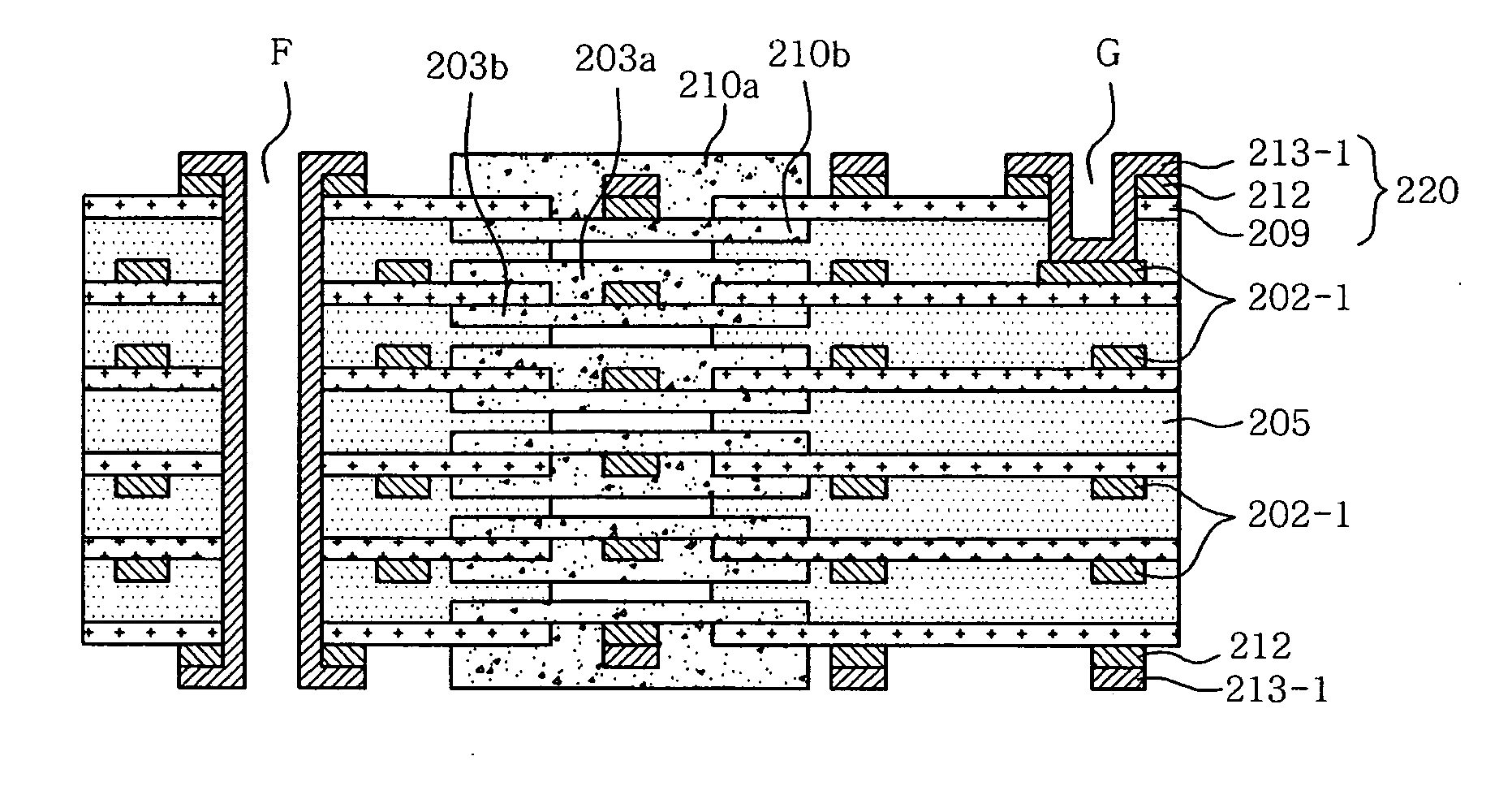
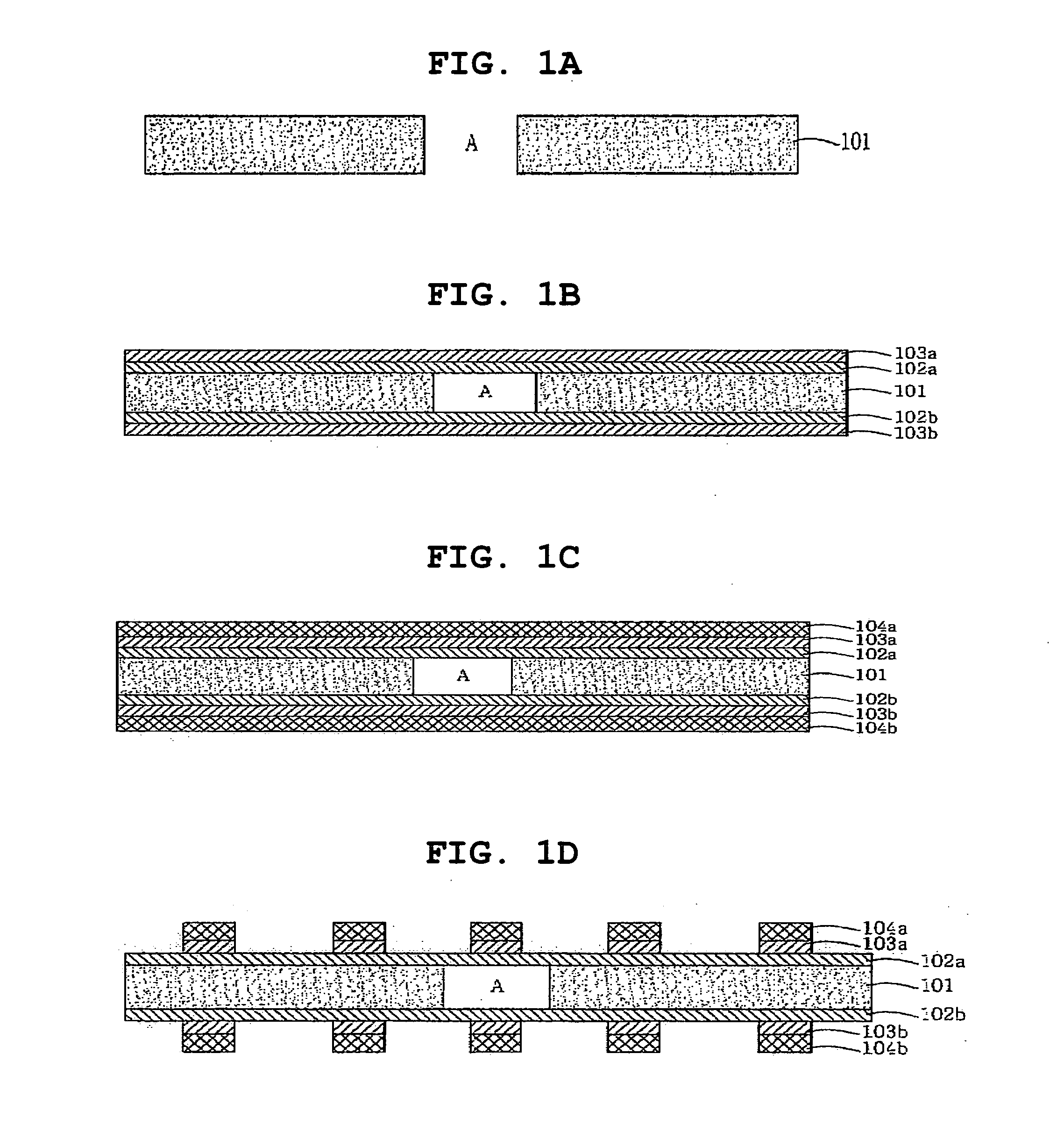
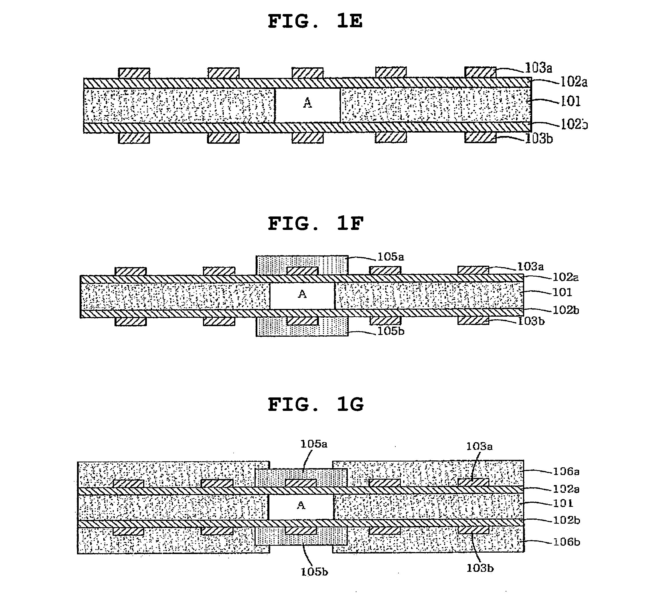
Rigid flexible printed circuit board and method of fabricating same
PatentInactiveUS20060193970A1
Innovation
- A method of fabricating rigid flexible PCBs without polyimide copper clad laminates, using prepregs and coverlays to form a laminate structure with excellent adhesion reliability and bendability, where the coverlay supports the flexible portion and connects rigid portions, eliminating the need for costly polyimide materials.

Manufacturing Standards and Quality Requirements Impact
Manufacturing standards and quality requirements significantly influence the development cost differential between microbump arrays and rigid-flex PCBs. The stringent precision demands of microbump technology necessitate adherence to advanced semiconductor manufacturing standards, including IPC-2221 for high-density interconnects and JEDEC specifications for bump pitch tolerances typically ranging from 20-50 micrometers. These requirements mandate specialized cleanroom environments with Class 10 or better contamination control, driving substantial infrastructure investments.
Quality assurance protocols for microbump arrays require sophisticated inspection methodologies, including automated optical inspection systems capable of sub-micron resolution and X-ray tomography for void detection. The implementation of statistical process control becomes critical due to the technology's sensitivity to manufacturing variations. Yield optimization demands extensive process characterization, with typical qualification cycles extending 12-18 months compared to 6-9 months for conventional interconnect technologies.
Rigid-flex PCB manufacturing operates under established IPC-6013 standards with well-defined quality metrics for bend radius, layer registration, and via reliability. The mature manufacturing ecosystem enables standardized testing procedures using conventional electrical testing equipment and mechanical stress analysis tools. Quality requirements focus primarily on lamination integrity and copper trace continuity, utilizing proven inspection techniques that require minimal additional capital investment.
The regulatory compliance landscape further impacts cost structures. Microbump arrays must satisfy stringent automotive and aerospace qualification standards, including AEC-Q100 for automotive applications, requiring extensive reliability testing across temperature cycling, mechanical shock, and humidity exposure. These qualification processes can consume 15-25% of total development budgets due to the extended testing duration and specialized equipment requirements.
Manufacturing yield considerations create additional cost pressures. Microbump arrays typically achieve 70-85% yield rates during initial production phases, compared to 90-95% for established rigid-flex processes. The defect density sensitivity of microbump technology requires implementation of advanced process monitoring systems, including real-time statistical process control and predictive maintenance protocols, adding 10-15% to manufacturing overhead costs.
Quality documentation and traceability requirements for microbump arrays demand comprehensive process genealogy tracking, from substrate preparation through final assembly. This necessitates investment in manufacturing execution systems capable of lot-level traceability, contributing to higher operational complexity and associated development costs compared to conventional rigid-flex manufacturing approaches.
Quality assurance protocols for microbump arrays require sophisticated inspection methodologies, including automated optical inspection systems capable of sub-micron resolution and X-ray tomography for void detection. The implementation of statistical process control becomes critical due to the technology's sensitivity to manufacturing variations. Yield optimization demands extensive process characterization, with typical qualification cycles extending 12-18 months compared to 6-9 months for conventional interconnect technologies.
Rigid-flex PCB manufacturing operates under established IPC-6013 standards with well-defined quality metrics for bend radius, layer registration, and via reliability. The mature manufacturing ecosystem enables standardized testing procedures using conventional electrical testing equipment and mechanical stress analysis tools. Quality requirements focus primarily on lamination integrity and copper trace continuity, utilizing proven inspection techniques that require minimal additional capital investment.
The regulatory compliance landscape further impacts cost structures. Microbump arrays must satisfy stringent automotive and aerospace qualification standards, including AEC-Q100 for automotive applications, requiring extensive reliability testing across temperature cycling, mechanical shock, and humidity exposure. These qualification processes can consume 15-25% of total development budgets due to the extended testing duration and specialized equipment requirements.
Manufacturing yield considerations create additional cost pressures. Microbump arrays typically achieve 70-85% yield rates during initial production phases, compared to 90-95% for established rigid-flex processes. The defect density sensitivity of microbump technology requires implementation of advanced process monitoring systems, including real-time statistical process control and predictive maintenance protocols, adding 10-15% to manufacturing overhead costs.
Quality documentation and traceability requirements for microbump arrays demand comprehensive process genealogy tracking, from substrate preparation through final assembly. This necessitates investment in manufacturing execution systems capable of lot-level traceability, contributing to higher operational complexity and associated development costs compared to conventional rigid-flex manufacturing approaches.
Supply Chain Cost Factors in Advanced PCB Production
The supply chain cost structure for advanced PCB production involving microbump arrays and rigid-flex technologies presents distinct economic challenges that significantly impact development budgets. Raw material procurement represents the most substantial cost differential between these technologies, with microbump arrays requiring specialized solder alloys, underfill materials, and high-purity substrates that command premium pricing due to limited supplier networks. Rigid-flex PCBs demand multi-layer flexible polyimide films, specialized adhesives, and copper foils with enhanced flexibility characteristics, creating dependency on specialized material suppliers with concentrated market power.
Manufacturing equipment requirements create substantial capital expenditure disparities across the supply chain. Microbump array production necessitates advanced lithography systems, precision placement equipment, and specialized reflow ovens capable of handling ultra-fine pitch components. The limited availability of such equipment from qualified suppliers results in extended lead times and elevated procurement costs. Conversely, rigid-flex PCB manufacturing requires sequential lamination presses, laser drilling systems, and flexible circuit handling equipment, representing a different but equally significant capital investment profile.
Supplier qualification and certification processes introduce additional cost layers that vary significantly between technologies. Microbump array suppliers must demonstrate capability in semiconductor-grade manufacturing processes, requiring extensive qualification periods and ongoing quality audits that increase per-unit costs. The limited global supplier base for critical materials and processes creates supply chain concentration risks that translate into premium pricing structures.
Geographic distribution of specialized suppliers further influences cost structures, with microbump array materials predominantly sourced from Asian semiconductor hubs, while rigid-flex materials maintain broader global availability. Transportation costs, inventory carrying expenses, and supply chain risk mitigation strategies create different economic models for each technology path.
Volume economics play crucial roles in determining supply chain cost effectiveness. Microbump arrays benefit from semiconductor industry scale economies but require minimum order quantities that may exceed typical PCB production volumes. Rigid-flex PCBs leverage established PCB industry supply chains but face material cost premiums for specialized flexible substrates and processing chemicals.
Quality assurance and testing requirements impose varying supply chain costs, with microbump arrays demanding advanced inspection equipment and materials traceability systems that increase supplier overhead costs. These factors collectively create distinct supply chain cost profiles that significantly influence technology selection decisions in advanced PCB development projects.
Manufacturing equipment requirements create substantial capital expenditure disparities across the supply chain. Microbump array production necessitates advanced lithography systems, precision placement equipment, and specialized reflow ovens capable of handling ultra-fine pitch components. The limited availability of such equipment from qualified suppliers results in extended lead times and elevated procurement costs. Conversely, rigid-flex PCB manufacturing requires sequential lamination presses, laser drilling systems, and flexible circuit handling equipment, representing a different but equally significant capital investment profile.
Supplier qualification and certification processes introduce additional cost layers that vary significantly between technologies. Microbump array suppliers must demonstrate capability in semiconductor-grade manufacturing processes, requiring extensive qualification periods and ongoing quality audits that increase per-unit costs. The limited global supplier base for critical materials and processes creates supply chain concentration risks that translate into premium pricing structures.
Geographic distribution of specialized suppliers further influences cost structures, with microbump array materials predominantly sourced from Asian semiconductor hubs, while rigid-flex materials maintain broader global availability. Transportation costs, inventory carrying expenses, and supply chain risk mitigation strategies create different economic models for each technology path.
Volume economics play crucial roles in determining supply chain cost effectiveness. Microbump arrays benefit from semiconductor industry scale economies but require minimum order quantities that may exceed typical PCB production volumes. Rigid-flex PCBs leverage established PCB industry supply chains but face material cost premiums for specialized flexible substrates and processing chemicals.
Quality assurance and testing requirements impose varying supply chain costs, with microbump arrays demanding advanced inspection equipment and materials traceability systems that increase supplier overhead costs. These factors collectively create distinct supply chain cost profiles that significantly influence technology selection decisions in advanced PCB development projects.
Unlock deeper insights with PatSnap Eureka Quick Research — get a full tech report to explore trends and direct your research. Try now!
Generate Your Research Report Instantly with AI Agent
Supercharge your innovation with PatSnap Eureka AI Agent Platform!