

Optimizing Solder Techniques for Microbump Arrays' Reliability
APR 22, 20269 MIN READ
Generate Your Research Report Instantly with AI Agent
PatSnap Eureka helps you evaluate technical feasibility & market potential.
Microbump Solder Technology Background and Objectives
Microbump technology emerged as a critical interconnect solution in the early 2000s to address the increasing demands for miniaturization and performance enhancement in advanced semiconductor packaging. This technology represents a paradigm shift from traditional wire bonding and flip-chip approaches, enabling three-dimensional integration and heterogeneous system assembly with unprecedented density and electrical performance.
The evolution of microbump arrays has been driven by the relentless pursuit of Moore's Law continuation through advanced packaging techniques. As semiconductor feature sizes approached physical limits, the industry pivoted toward More-than-Moore strategies, where microbumps serve as the fundamental building blocks for 2.5D and 3D integrated circuits. These microscale solder interconnects, typically ranging from 10 to 50 micrometers in diameter, facilitate high-density connections between dies, substrates, and interposers.
Historical development traces back to IBM's pioneering work on C4 technology, which laid the groundwork for controlled collapse chip connection methodologies. The transition from traditional solder bumps to microbumps was necessitated by the need for finer pitch interconnects, reduced parasitic effects, and improved thermal management in high-performance computing applications. Key technological milestones include the introduction of copper pillar microbumps, lead-free solder compositions, and advanced underfill materials.
Current technological objectives center on achieving exceptional reliability performance under increasingly demanding operational conditions. Primary goals include minimizing electromigration effects, enhancing thermal cycling resistance, and maintaining mechanical integrity under high-frequency switching loads. The industry targets achieving mean time to failure exceeding 10 years under accelerated stress conditions while maintaining electrical resistance below specified thresholds.
Reliability optimization encompasses multiple interdisciplinary challenges, including solder alloy composition refinement, reflow profile optimization, and interfacial metallurgy control. The objective extends beyond mere mechanical connection to ensuring signal integrity, power delivery efficiency, and thermal dissipation effectiveness. Advanced characterization techniques and predictive modeling approaches are being developed to understand failure mechanisms and establish design guidelines for next-generation microbump arrays in emerging applications such as artificial intelligence processors and high-bandwidth memory interfaces.
The evolution of microbump arrays has been driven by the relentless pursuit of Moore's Law continuation through advanced packaging techniques. As semiconductor feature sizes approached physical limits, the industry pivoted toward More-than-Moore strategies, where microbumps serve as the fundamental building blocks for 2.5D and 3D integrated circuits. These microscale solder interconnects, typically ranging from 10 to 50 micrometers in diameter, facilitate high-density connections between dies, substrates, and interposers.
Historical development traces back to IBM's pioneering work on C4 technology, which laid the groundwork for controlled collapse chip connection methodologies. The transition from traditional solder bumps to microbumps was necessitated by the need for finer pitch interconnects, reduced parasitic effects, and improved thermal management in high-performance computing applications. Key technological milestones include the introduction of copper pillar microbumps, lead-free solder compositions, and advanced underfill materials.
Current technological objectives center on achieving exceptional reliability performance under increasingly demanding operational conditions. Primary goals include minimizing electromigration effects, enhancing thermal cycling resistance, and maintaining mechanical integrity under high-frequency switching loads. The industry targets achieving mean time to failure exceeding 10 years under accelerated stress conditions while maintaining electrical resistance below specified thresholds.
Reliability optimization encompasses multiple interdisciplinary challenges, including solder alloy composition refinement, reflow profile optimization, and interfacial metallurgy control. The objective extends beyond mere mechanical connection to ensuring signal integrity, power delivery efficiency, and thermal dissipation effectiveness. Advanced characterization techniques and predictive modeling approaches are being developed to understand failure mechanisms and establish design guidelines for next-generation microbump arrays in emerging applications such as artificial intelligence processors and high-bandwidth memory interfaces.
Market Demand for Advanced Microbump Packaging Solutions
The semiconductor packaging industry is experiencing unprecedented demand for advanced microbump packaging solutions, driven by the relentless pursuit of miniaturization and performance enhancement in electronic devices. Consumer electronics manufacturers are increasingly adopting three-dimensional integrated circuits and system-in-package architectures, creating substantial market opportunities for microbump technologies that enable higher interconnect densities and improved electrical performance.
Mobile device manufacturers represent the largest consumer segment for advanced microbump packaging solutions. The continuous evolution toward thinner smartphones, tablets, and wearable devices necessitates packaging technologies that can accommodate multiple functional blocks within severely constrained form factors. Microbump arrays provide the essential interconnect density required for stacking memory modules, processors, and specialized chips in compact configurations.
The automotive electronics sector is emerging as a significant growth driver for microbump packaging demand. Advanced driver assistance systems, autonomous vehicle technologies, and electric vehicle power management systems require highly reliable interconnect solutions capable of withstanding extreme temperature variations and mechanical stress. These applications demand microbump technologies with enhanced solder joint reliability and long-term durability.
Data center and high-performance computing applications are generating substantial demand for microbump packaging solutions that can support high-bandwidth memory interfaces and multi-core processor architectures. The increasing computational requirements for artificial intelligence, machine learning, and cloud computing services are driving the need for packaging technologies that enable efficient heat dissipation while maintaining signal integrity across dense interconnect arrays.
The telecommunications infrastructure market, particularly with the deployment of fifth-generation wireless networks, is creating new opportunities for advanced microbump packaging. Base station equipment, network processors, and radio frequency components require packaging solutions that can handle high-frequency signals while maintaining thermal stability and mechanical reliability under continuous operation conditions.
Medical device manufacturers are increasingly adopting microbump packaging for implantable devices, diagnostic equipment, and portable monitoring systems. These applications demand packaging solutions with exceptional reliability and biocompatibility, driving the need for optimized solder techniques that ensure long-term performance in challenging biological environments.
The aerospace and defense sectors represent specialized but lucrative markets for advanced microbump packaging solutions. These applications require packaging technologies that can withstand extreme environmental conditions, radiation exposure, and mechanical shock while maintaining critical system functionality over extended operational lifespans.
Mobile device manufacturers represent the largest consumer segment for advanced microbump packaging solutions. The continuous evolution toward thinner smartphones, tablets, and wearable devices necessitates packaging technologies that can accommodate multiple functional blocks within severely constrained form factors. Microbump arrays provide the essential interconnect density required for stacking memory modules, processors, and specialized chips in compact configurations.
The automotive electronics sector is emerging as a significant growth driver for microbump packaging demand. Advanced driver assistance systems, autonomous vehicle technologies, and electric vehicle power management systems require highly reliable interconnect solutions capable of withstanding extreme temperature variations and mechanical stress. These applications demand microbump technologies with enhanced solder joint reliability and long-term durability.
Data center and high-performance computing applications are generating substantial demand for microbump packaging solutions that can support high-bandwidth memory interfaces and multi-core processor architectures. The increasing computational requirements for artificial intelligence, machine learning, and cloud computing services are driving the need for packaging technologies that enable efficient heat dissipation while maintaining signal integrity across dense interconnect arrays.
The telecommunications infrastructure market, particularly with the deployment of fifth-generation wireless networks, is creating new opportunities for advanced microbump packaging. Base station equipment, network processors, and radio frequency components require packaging solutions that can handle high-frequency signals while maintaining thermal stability and mechanical reliability under continuous operation conditions.
Medical device manufacturers are increasingly adopting microbump packaging for implantable devices, diagnostic equipment, and portable monitoring systems. These applications demand packaging solutions with exceptional reliability and biocompatibility, driving the need for optimized solder techniques that ensure long-term performance in challenging biological environments.
The aerospace and defense sectors represent specialized but lucrative markets for advanced microbump packaging solutions. These applications require packaging technologies that can withstand extreme environmental conditions, radiation exposure, and mechanical shock while maintaining critical system functionality over extended operational lifespans.
Current Microbump Solder Reliability Challenges and Status
Microbump solder reliability faces significant challenges in modern semiconductor packaging, particularly as device miniaturization continues to push the boundaries of interconnect technology. The primary reliability concerns stem from the inherent mechanical and thermal stresses imposed on these ultra-small solder joints, which typically measure between 10-50 micrometers in diameter. These microscopic connections must maintain electrical continuity and mechanical integrity throughout the device lifecycle while experiencing repeated thermal cycling, mechanical shock, and environmental exposure.
Thermal cycling represents one of the most critical reliability challenges for microbump arrays. The coefficient of thermal expansion mismatch between different materials in the package assembly creates cyclic stress concentrations at the solder joint interfaces. This phenomenon leads to fatigue crack initiation and propagation, ultimately resulting in electrical failure. Current industry data indicates that microbump solder joints exhibit significantly reduced thermal cycling performance compared to conventional flip-chip bumps, with failure rates increasing exponentially as bump pitch decreases below 40 micrometers.
Electromigration poses another substantial reliability concern, particularly in high-current density applications. The reduced cross-sectional area of microbumps concentrates current flow, accelerating atomic migration within the solder matrix. This process causes void formation and metal depletion, leading to resistance increases and eventual open circuits. Advanced packaging applications requiring higher power densities exacerbate this challenge, as current densities can exceed 10^5 A/cm² in some microbump configurations.
Manufacturing-induced defects significantly impact microbump reliability, with process variations becoming more pronounced at smaller scales. Solder volume inconsistencies, underfill voids, and intermetallic compound formation irregularities create reliability weak points throughout the array. Non-destructive testing methods struggle to detect these microscopic defects, making quality control increasingly challenging as bump sizes continue to shrink.
The current technological status reveals that traditional solder alloys and processing techniques are approaching their fundamental limits for microbump applications. Lead-free solder systems, while environmentally compliant, exhibit inferior mechanical properties compared to legacy lead-based alloys, particularly in terms of fatigue resistance and creep behavior. Industry leaders are actively investigating alternative materials and novel processing approaches to address these limitations.
Recent developments in solder paste formulations and reflow profile optimization have shown promising improvements in microbump reliability. Advanced flux chemistries and controlled atmosphere processing help minimize oxidation and improve wetting characteristics. However, these incremental improvements may not be sufficient to meet the reliability requirements of next-generation packaging technologies, necessitating more fundamental innovations in materials and processing methodologies.
Thermal cycling represents one of the most critical reliability challenges for microbump arrays. The coefficient of thermal expansion mismatch between different materials in the package assembly creates cyclic stress concentrations at the solder joint interfaces. This phenomenon leads to fatigue crack initiation and propagation, ultimately resulting in electrical failure. Current industry data indicates that microbump solder joints exhibit significantly reduced thermal cycling performance compared to conventional flip-chip bumps, with failure rates increasing exponentially as bump pitch decreases below 40 micrometers.
Electromigration poses another substantial reliability concern, particularly in high-current density applications. The reduced cross-sectional area of microbumps concentrates current flow, accelerating atomic migration within the solder matrix. This process causes void formation and metal depletion, leading to resistance increases and eventual open circuits. Advanced packaging applications requiring higher power densities exacerbate this challenge, as current densities can exceed 10^5 A/cm² in some microbump configurations.
Manufacturing-induced defects significantly impact microbump reliability, with process variations becoming more pronounced at smaller scales. Solder volume inconsistencies, underfill voids, and intermetallic compound formation irregularities create reliability weak points throughout the array. Non-destructive testing methods struggle to detect these microscopic defects, making quality control increasingly challenging as bump sizes continue to shrink.
The current technological status reveals that traditional solder alloys and processing techniques are approaching their fundamental limits for microbump applications. Lead-free solder systems, while environmentally compliant, exhibit inferior mechanical properties compared to legacy lead-based alloys, particularly in terms of fatigue resistance and creep behavior. Industry leaders are actively investigating alternative materials and novel processing approaches to address these limitations.
Recent developments in solder paste formulations and reflow profile optimization have shown promising improvements in microbump reliability. Advanced flux chemistries and controlled atmosphere processing help minimize oxidation and improve wetting characteristics. However, these incremental improvements may not be sufficient to meet the reliability requirements of next-generation packaging technologies, necessitating more fundamental innovations in materials and processing methodologies.
Existing Microbump Solder Optimization Techniques
01 Underfill materials and processes for microbump reliability
The use of underfill materials between microbump arrays and substrates is critical for enhancing mechanical strength and reliability. Underfill processes involve dispensing polymer materials that flow between bumps to provide stress relief, prevent crack propagation, and protect against moisture ingress. The composition, viscosity, and curing parameters of underfill materials are optimized to ensure complete filling without voids while maintaining compatibility with the solder alloy and substrate materials.- Underfill materials and processes for microbump reliability: The use of underfill materials between microbump arrays and substrates is critical for enhancing mechanical strength and reliability. Underfill processes involve dispensing polymer materials that flow between bumps to provide stress relief, prevent crack propagation, and protect against moisture ingress. The composition, viscosity, and curing parameters of underfill materials are optimized to ensure complete filling without voids while maintaining compatibility with the solder alloy and substrate materials.
- Solder alloy composition optimization for microbumps: The selection and formulation of solder alloy compositions significantly impact the reliability of microbump interconnections. Lead-free solder alloys with specific compositions are developed to provide appropriate melting temperatures, wetting characteristics, and intermetallic compound formation. The alloy composition affects electromigration resistance, thermal cycling performance, and mechanical properties of the solder joints. Additives and dopants are incorporated to refine grain structure and improve long-term reliability.
- Reflow profile and temperature control techniques: Precise control of reflow soldering profiles is essential for achieving reliable microbump connections. The reflow process parameters including peak temperature, time above liquidus, heating and cooling rates are carefully controlled to ensure proper solder wetting and minimize void formation. Multiple reflow stages may be employed for complex assemblies. Temperature uniformity across the array and thermal management strategies prevent warpage and ensure consistent joint formation across all microbumps.
- Microbump structure design and metallization layers: The physical design of microbump structures including bump height, diameter, pitch, and metallization stack significantly influences reliability. Under-bump metallization layers serve as diffusion barriers and adhesion promoters between the solder and substrate. The metallization scheme typically includes multiple layers with specific functions such as preventing intermetallic growth and providing electrical conductivity. Bump geometry is optimized to balance electrical performance with mechanical reliability under thermal and mechanical stress.
- Reliability testing and failure analysis methods: Comprehensive reliability testing protocols are employed to evaluate microbump array performance under various stress conditions. Testing methods include thermal cycling, high temperature storage, humidity exposure, and electromigration testing to simulate real-world operating conditions. Failure analysis techniques such as cross-sectioning, scanning electron microscopy, and X-ray inspection identify failure modes including crack formation, delamination, and intermetallic growth. These assessments guide process improvements and design modifications to enhance long-term reliability.
02 Solder alloy composition optimization for microbumps
The selection and formulation of solder alloy compositions significantly impact the reliability of microbump interconnections. Lead-free solder alloys with specific compositions are developed to provide appropriate melting temperatures, wetting characteristics, and intermetallic compound formation. The alloy composition affects electromigration resistance, thermal cycling performance, and mechanical properties of the solder joints. Additives and dopants are incorporated to refine grain structure and improve long-term reliability.Expand Specific Solutions03 Reflow profile and temperature control techniques
Precise control of reflow soldering profiles is essential for achieving reliable microbump connections. The reflow process parameters including peak temperature, time above liquidus, heating and cooling rates are carefully controlled to ensure proper solder wetting and minimize void formation. Multiple reflow stages may be employed for complex assemblies. Temperature uniformity across the array and thermal management strategies prevent warpage and ensure consistent joint formation across all microbumps in the array.Expand Specific Solutions04 Microbump structure design and metallization layers
The physical design of microbump structures including bump height, diameter, pitch, and metallization stack affects reliability. Under-bump metallization layers serve as diffusion barriers and adhesion promoters between the solder and substrate. The metallization scheme typically includes multiple layers with specific functions such as preventing intermetallic growth and providing mechanical support. Bump geometry is optimized to balance electrical performance with mechanical reliability under thermal and mechanical stress.Expand Specific Solutions05 Reliability testing and failure analysis methods
Comprehensive reliability testing protocols are employed to evaluate microbump array performance under various stress conditions. Testing methods include thermal cycling, temperature humidity bias, and mechanical shock tests to simulate real-world operating conditions. Advanced inspection techniques such as X-ray imaging and acoustic microscopy detect voids, cracks, and delamination. Accelerated life testing and failure analysis provide data for predicting long-term reliability and identifying failure mechanisms such as electromigration, fatigue, and intermetallic compound growth.Expand Specific Solutions
Key Players in Microbump and Advanced Packaging Industry
The microbump array solder optimization market represents a rapidly evolving segment within advanced semiconductor packaging, driven by increasing demand for miniaturization and higher performance in electronics. The industry is in a growth phase, with significant market expansion expected as 5G, AI, and IoT applications proliferate. Technology maturity varies considerably across players, with established semiconductor giants like Intel, TSMC, and AMD leading in production-scale implementation, while specialized companies such as STATS ChipPAC and National Center for Advanced Packaging focus on advanced packaging solutions. Research institutions like Imec and universities including Peking University contribute foundational innovations. Industrial conglomerates like Siemens and Panasonic integrate these technologies into broader manufacturing ecosystems. The competitive landscape shows a clear division between technology developers, manufacturing specialists, and end-user integrators, with Asian companies particularly strong in packaging services and European firms excelling in equipment and materials development.
Intel Corp.
Technical Solution: Intel has pioneered hybrid bonding techniques combined with traditional solder microbumps for heterogeneous integration. Their technology focuses on low-temperature solder alloys (SAC305) with enhanced wetting properties through surface treatment optimization. Intel's approach includes real-time process monitoring using machine learning algorithms to predict and prevent solder joint failures, incorporating stress-aware design methodologies and advanced thermal interface materials for improved reliability in high-performance computing applications.
Strengths: Strong R&D capabilities and advanced packaging expertise for high-performance applications. Weaknesses: Limited manufacturing capacity compared to pure-play foundries and higher cost structure.
Taiwan Semiconductor Manufacturing Co., Ltd.
Technical Solution: TSMC has developed advanced microbump soldering techniques utilizing copper pillar bumps with controlled collapse chip connection (C4) technology. Their approach incorporates precise thermal management during reflow processes, achieving bump pitch scaling down to 40μm with enhanced reliability through optimized underfill materials and multi-step thermal cycling validation. The company employs advanced flux chemistry and nitrogen atmosphere reflow to minimize voiding and ensure consistent joint formation across large die areas.
Strengths: Industry-leading manufacturing scale and process control capabilities. Weaknesses: High capital investment requirements and complex process integration challenges.
Core Patents in Microbump Reliability Enhancement
Method of fabricating solder bumps
PatentActiveUS20090181223A1
Innovation
- A two-step injection molded solder (IMS) process forming a two-layered Pb-free solder structure with a high melting temperature solder followed by a low melting temperature solder, ensuring effective multi-chip module assembly and reliability, reducing UBM consumption, and providing a greater stand-off height and flexibility in alloy composition.
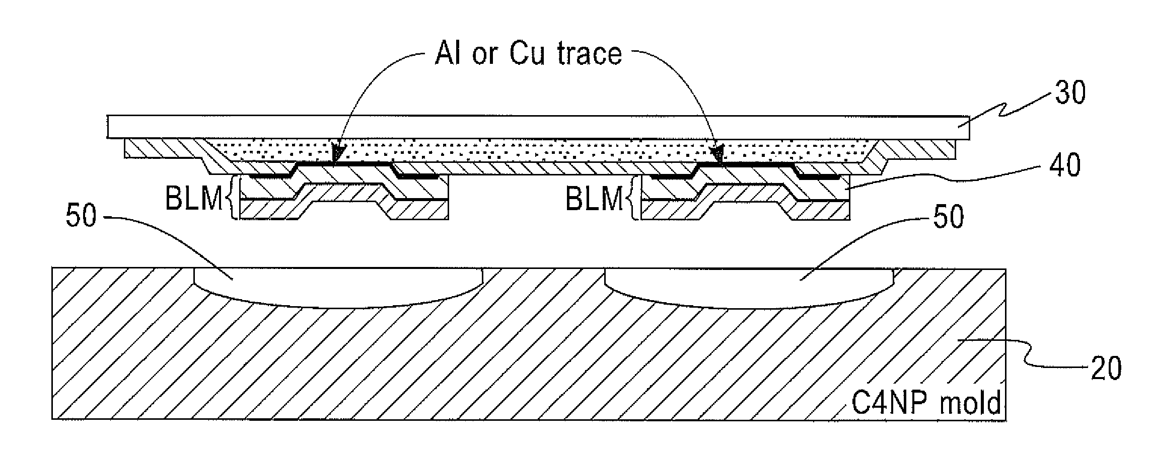
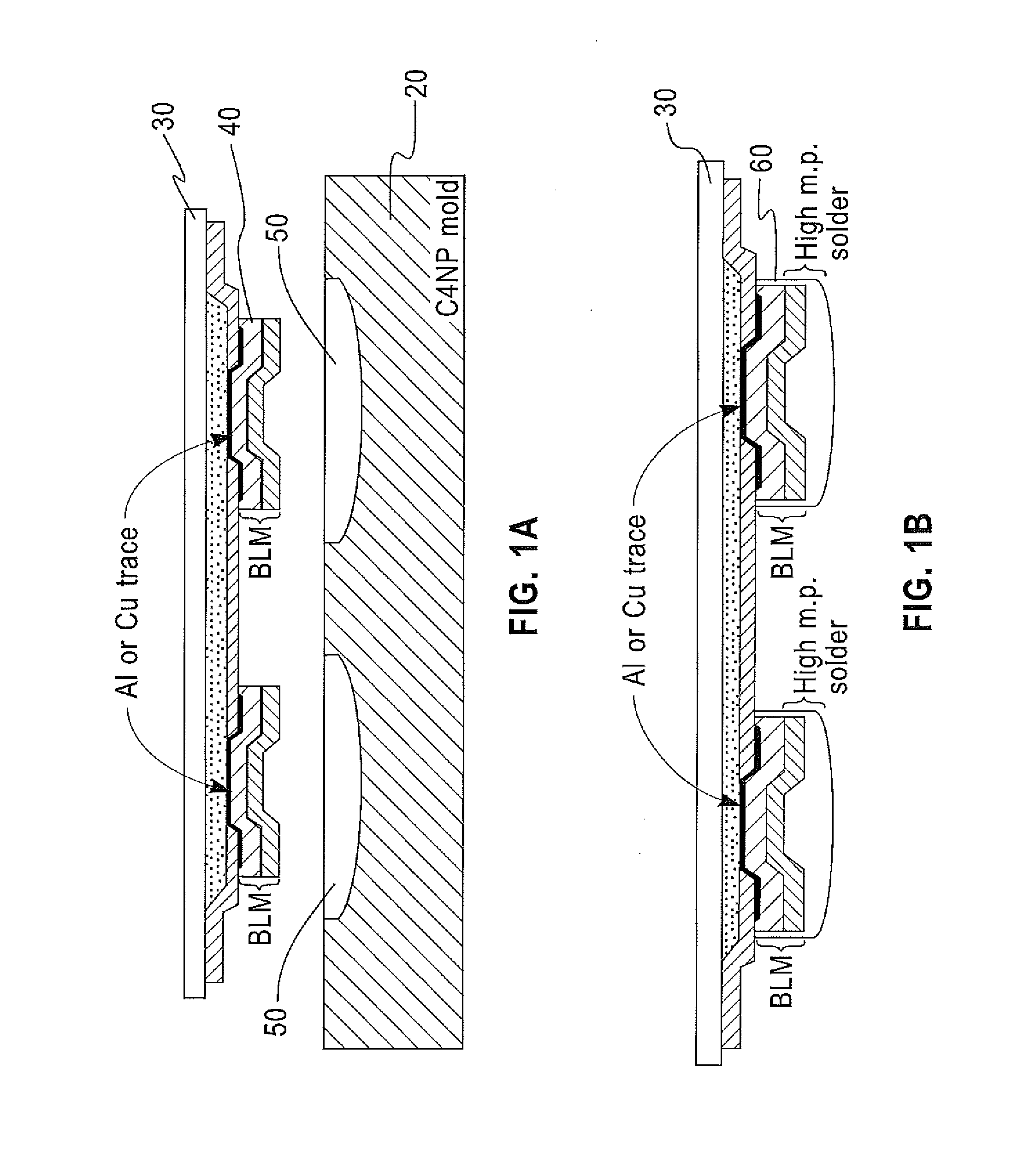
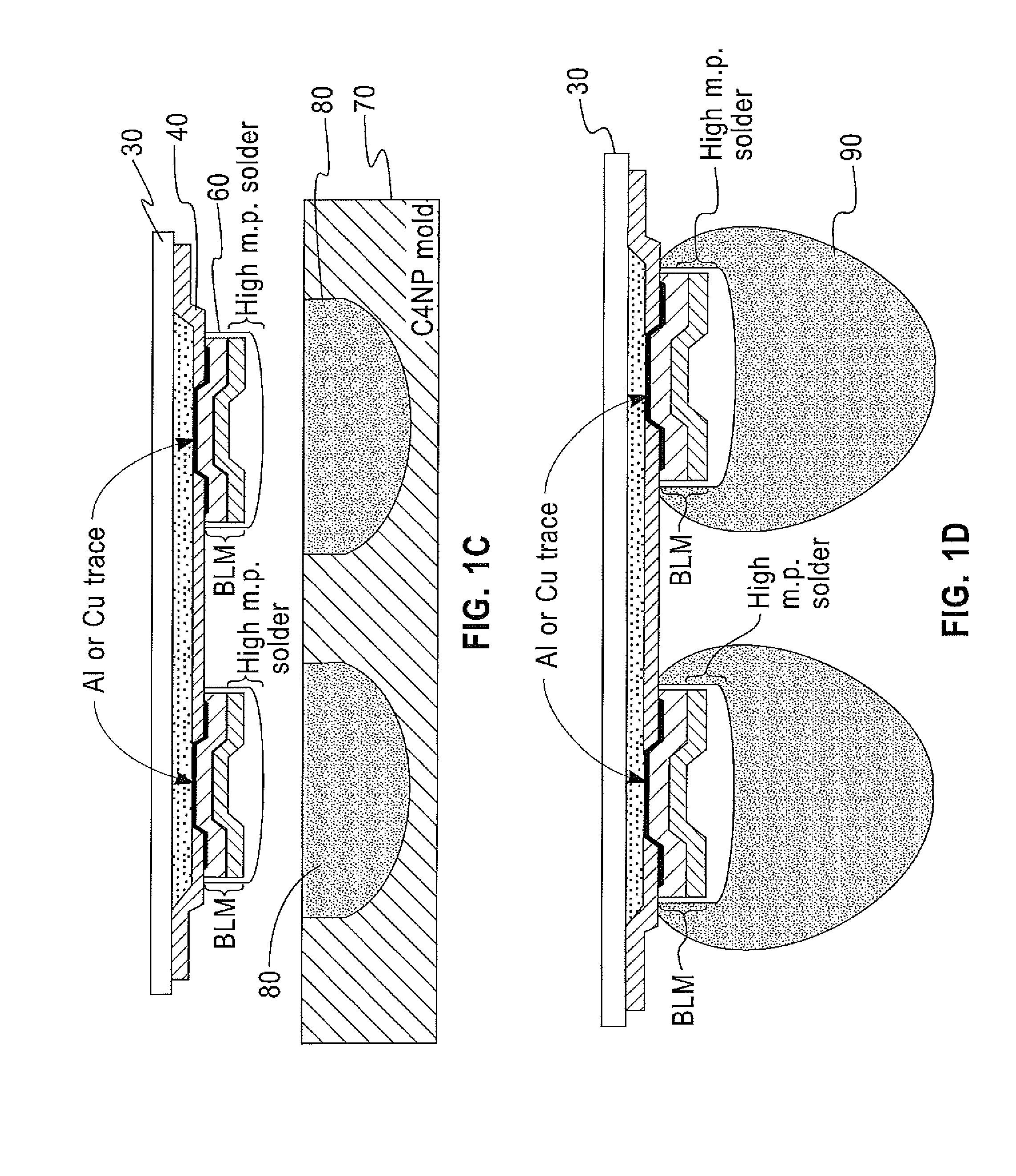

Increased solder-bump height for improved flip-chip bonding and reliability
PatentInactiveUS6596618B1
Innovation
- A method involving a two-level solder bump precursor structure is formed by depositing a first layer of solder into patterned holes in a photoresist layer, followed by a second layer of solder with a smaller diameter on top, which is then reflowed to create taller, spherical solder bumps without the formation of mushroom-shaped overhangs that can trap photoresist residue.


Thermal Management Strategies for Microbump Arrays
Thermal management represents a critical aspect of microbump array optimization, as excessive heat generation and inadequate dissipation directly impact solder joint reliability and overall system performance. The miniaturized nature of microbump structures, typically ranging from 10 to 50 micrometers in diameter, creates unique thermal challenges that require specialized management strategies to ensure long-term operational stability.
The primary thermal concern in microbump arrays stems from current crowding effects and Joule heating within the confined solder volumes. As electrical current passes through these microscopic interconnects, resistance-induced heating can cause localized temperature spikes that exceed the solder's thermal tolerance. This phenomenon is particularly pronounced in high-density arrays where thermal dissipation pathways are limited by the reduced spacing between adjacent bumps.
Effective thermal management strategies must address both heat generation and dissipation mechanisms. Advanced underfill materials with enhanced thermal conductivity, typically incorporating ceramic fillers or carbon nanotubes, provide improved heat transfer pathways from the solder joints to the substrate. These materials maintain electrical insulation while offering thermal conductivity values exceeding 2 W/mK, significantly higher than conventional underfills.
Substrate-level thermal management involves implementing thermal vias and heat spreaders strategically positioned beneath high-current microbump clusters. Copper-filled through-silicon vias (TSVs) create vertical thermal conduction paths, while integrated heat spreaders distribute thermal loads across larger substrate areas. The thermal interface between the die and package substrate requires careful optimization to minimize thermal resistance.
Active thermal management solutions include micro-scale heat sinks and embedded cooling channels within the package structure. These approaches become essential for high-power applications where passive thermal management proves insufficient. Computational fluid dynamics modeling helps optimize coolant flow patterns and heat sink geometries for maximum thermal efficiency.
Temperature monitoring and control systems enable real-time thermal management through embedded sensors and adaptive power management algorithms. These systems can detect thermal hotspots and implement corrective measures before solder joint degradation occurs, extending the operational lifetime of microbump arrays in demanding thermal environments.
The primary thermal concern in microbump arrays stems from current crowding effects and Joule heating within the confined solder volumes. As electrical current passes through these microscopic interconnects, resistance-induced heating can cause localized temperature spikes that exceed the solder's thermal tolerance. This phenomenon is particularly pronounced in high-density arrays where thermal dissipation pathways are limited by the reduced spacing between adjacent bumps.
Effective thermal management strategies must address both heat generation and dissipation mechanisms. Advanced underfill materials with enhanced thermal conductivity, typically incorporating ceramic fillers or carbon nanotubes, provide improved heat transfer pathways from the solder joints to the substrate. These materials maintain electrical insulation while offering thermal conductivity values exceeding 2 W/mK, significantly higher than conventional underfills.
Substrate-level thermal management involves implementing thermal vias and heat spreaders strategically positioned beneath high-current microbump clusters. Copper-filled through-silicon vias (TSVs) create vertical thermal conduction paths, while integrated heat spreaders distribute thermal loads across larger substrate areas. The thermal interface between the die and package substrate requires careful optimization to minimize thermal resistance.
Active thermal management solutions include micro-scale heat sinks and embedded cooling channels within the package structure. These approaches become essential for high-power applications where passive thermal management proves insufficient. Computational fluid dynamics modeling helps optimize coolant flow patterns and heat sink geometries for maximum thermal efficiency.
Temperature monitoring and control systems enable real-time thermal management through embedded sensors and adaptive power management algorithms. These systems can detect thermal hotspots and implement corrective measures before solder joint degradation occurs, extending the operational lifetime of microbump arrays in demanding thermal environments.
Quality Control Standards for Microbump Manufacturing
Quality control standards for microbump manufacturing represent a critical framework that ensures consistent performance and reliability in advanced semiconductor packaging applications. These standards encompass comprehensive measurement protocols, inspection methodologies, and acceptance criteria that govern the production of microbumps with diameters typically ranging from 10 to 50 micrometers. The establishment of rigorous quality control measures becomes increasingly vital as device miniaturization demands higher interconnect densities and enhanced electrical performance.
Dimensional accuracy standards form the foundation of microbump quality control, requiring precise measurement of bump height, diameter, and pitch uniformity across entire wafer surfaces. Advanced metrology systems utilizing white light interferometry and scanning electron microscopy enable sub-micrometer measurement precision, with typical tolerance specifications maintaining height variations within ±2 micrometers and diameter consistency within ±1 micrometer. These dimensional controls directly impact subsequent assembly processes and final device reliability.
Material composition verification represents another crucial aspect of quality standards, particularly for solder-based microbumps where tin-silver-copper alloy ratios must remain within specified ranges to ensure proper melting characteristics and intermetallic formation. X-ray fluorescence spectroscopy and energy-dispersive spectroscopy provide non-destructive composition analysis, with acceptance criteria typically requiring elemental concentrations within ±0.5% of target values.
Surface integrity assessment protocols evaluate microbump morphology, identifying potential defects such as voids, cracks, or oxidation that could compromise joint reliability. Automated optical inspection systems combined with machine learning algorithms enable high-throughput defect detection, categorizing anomalies based on severity levels and establishing rejection thresholds that balance yield optimization with reliability requirements.
Electrical continuity testing validates the fundamental interconnect function of microbumps through resistance measurements and current-carrying capacity verification. These tests employ specialized probe card technologies capable of contacting individual microbumps, with typical acceptance criteria requiring contact resistance below 50 milliohms and current handling capabilities exceeding 100 milliamperes per bump.
Statistical process control implementation ensures manufacturing consistency through real-time monitoring of key parameters and trend analysis. Control charts tracking bump height distribution, placement accuracy, and defect rates enable proactive process adjustments, maintaining production within established control limits and minimizing quality variations that could impact downstream assembly operations.
Dimensional accuracy standards form the foundation of microbump quality control, requiring precise measurement of bump height, diameter, and pitch uniformity across entire wafer surfaces. Advanced metrology systems utilizing white light interferometry and scanning electron microscopy enable sub-micrometer measurement precision, with typical tolerance specifications maintaining height variations within ±2 micrometers and diameter consistency within ±1 micrometer. These dimensional controls directly impact subsequent assembly processes and final device reliability.
Material composition verification represents another crucial aspect of quality standards, particularly for solder-based microbumps where tin-silver-copper alloy ratios must remain within specified ranges to ensure proper melting characteristics and intermetallic formation. X-ray fluorescence spectroscopy and energy-dispersive spectroscopy provide non-destructive composition analysis, with acceptance criteria typically requiring elemental concentrations within ±0.5% of target values.
Surface integrity assessment protocols evaluate microbump morphology, identifying potential defects such as voids, cracks, or oxidation that could compromise joint reliability. Automated optical inspection systems combined with machine learning algorithms enable high-throughput defect detection, categorizing anomalies based on severity levels and establishing rejection thresholds that balance yield optimization with reliability requirements.
Electrical continuity testing validates the fundamental interconnect function of microbumps through resistance measurements and current-carrying capacity verification. These tests employ specialized probe card technologies capable of contacting individual microbumps, with typical acceptance criteria requiring contact resistance below 50 milliohms and current handling capabilities exceeding 100 milliamperes per bump.
Statistical process control implementation ensures manufacturing consistency through real-time monitoring of key parameters and trend analysis. Control charts tracking bump height distribution, placement accuracy, and defect rates enable proactive process adjustments, maintaining production within established control limits and minimizing quality variations that could impact downstream assembly operations.
Unlock deeper insights with PatSnap Eureka Quick Research — get a full tech report to explore trends and direct your research. Try now!
Generate Your Research Report Instantly with AI Agent
Supercharge your innovation with PatSnap Eureka AI Agent Platform!