

Experiment Validity in Integrating Metal Nanostructures
APR 17, 20269 MIN READ
Generate Your Research Report Instantly with AI Agent
PatSnap Eureka helps you evaluate technical feasibility & market potential.
Metal Nanostructure Integration Background and Research Goals
Metal nanostructures have emerged as a transformative technology across multiple scientific and industrial domains, fundamentally altering how we approach materials engineering, electronics, and biomedical applications. The integration of these nanoscale metallic components represents a convergence of advanced synthesis techniques, precision manufacturing, and sophisticated characterization methods that have evolved significantly over the past three decades.
The historical development of metal nanostructure integration traces back to the early 1990s when researchers first demonstrated controlled synthesis of gold and silver nanoparticles. This foundational work established the groundwork for understanding size-dependent properties and surface effects that distinguish nanoscale metals from their bulk counterparts. The field experienced rapid acceleration in the 2000s with the advent of sophisticated lithographic techniques and self-assembly methods, enabling precise control over nanostructure geometry, composition, and spatial arrangement.
Current technological evolution focuses on achieving seamless integration of metal nanostructures into functional devices and systems while maintaining their unique properties. This integration challenge encompasses multiple scales, from atomic-level interface engineering to macroscopic device architecture. The complexity arises from the need to preserve quantum size effects, plasmonic properties, and enhanced surface reactivity while ensuring mechanical stability and electrical connectivity within larger systems.
The primary research objectives in metal nanostructure integration center on developing reliable methodologies for controlled placement, stable interfacial bonding, and predictable performance characteristics. Key goals include establishing standardized protocols for nanostructure synthesis with precise dimensional control, developing robust integration techniques that maintain structural integrity during processing, and creating comprehensive characterization frameworks to validate integration success.
Advanced applications driving current research include next-generation electronic devices leveraging quantum effects, plasmonic sensors with unprecedented sensitivity, and catalytic systems with enhanced efficiency. These applications demand integration approaches that can accommodate the unique physical and chemical properties of metal nanostructures while meeting stringent performance and reliability requirements.
The technological trajectory indicates a shift toward hybrid integration strategies that combine top-down and bottom-up approaches, enabling hierarchical assembly of complex nanostructured systems. Future developments aim to achieve deterministic control over nanostructure positioning, orientation, and connectivity, ultimately enabling the realization of novel functionalities that emerge from collective behavior of integrated nanostructure arrays.
Market Demand for Metal Nanostructure Applications
The integration of metal nanostructures represents a rapidly expanding market driven by diverse industrial applications and technological advancement needs. Electronics manufacturing constitutes the largest demand segment, where metal nanostructures enable miniaturization of components, enhanced conductivity, and improved performance in semiconductors, sensors, and flexible electronics. The semiconductor industry particularly drives demand for gold, silver, and copper nanostructures in interconnects and quantum dots applications.
Healthcare and biomedical sectors demonstrate substantial growth potential for metal nanostructure applications. Silver and gold nanoparticles find extensive use in antimicrobial coatings, drug delivery systems, diagnostic imaging, and therapeutic treatments. The increasing focus on personalized medicine and advanced diagnostic techniques continues to expand market opportunities in this domain.
Energy storage and conversion markets present significant demand for metal nanostructures in battery electrodes, fuel cells, and photovoltaic systems. Lithium-ion battery manufacturers increasingly incorporate silicon and metal oxide nanostructures to enhance energy density and charging efficiency. Solar panel production utilizes silver nanostructures for improved light absorption and electrical conductivity.
Catalysis applications across chemical processing, automotive, and environmental sectors drive consistent demand for platinum, palladium, and nickel nanostructures. These materials enable more efficient chemical reactions, reduced energy consumption, and enhanced selectivity in industrial processes. Automotive catalytic converters represent a mature but stable market segment.
The coatings and surface treatment industry increasingly adopts metal nanostructures for protective, decorative, and functional applications. Anti-corrosion coatings, wear-resistant surfaces, and smart materials incorporate various metal nanoparticles to achieve superior performance characteristics compared to conventional alternatives.
Market growth faces challenges including production scalability, cost optimization, and regulatory compliance requirements. Quality control and standardization remain critical factors influencing adoption rates across different industries. Environmental considerations and sustainability concerns increasingly influence purchasing decisions and product development strategies.
Regional demand patterns show concentration in Asia-Pacific manufacturing hubs, North American technology centers, and European automotive and chemical industries. Emerging applications in quantum computing, advanced sensors, and next-generation electronics promise to create new market segments and drive continued expansion in metal nanostructure integration technologies.
Current State and Experimental Challenges in Metal Nanointegration
The current landscape of metal nanostructure integration presents a complex array of technological achievements alongside persistent experimental challenges that continue to limit widespread commercial implementation. Contemporary research has successfully demonstrated the feasibility of incorporating various metallic nanoparticles, including gold, silver, platinum, and copper-based structures, into diverse host matrices ranging from polymeric substrates to semiconductor devices and biological systems.
Leading research institutions and technology companies have established sophisticated fabrication methodologies, including chemical vapor deposition, electrochemical synthesis, and self-assembly techniques. These approaches have enabled the production of metal nanostructures with controlled size distributions, typically ranging from 1 to 100 nanometers, and tailored surface functionalities. Current integration processes can achieve spatial precision at the sub-micrometer scale, facilitating applications in advanced electronics, catalysis, and sensing technologies.
However, significant experimental challenges persist in validating the reliability and reproducibility of integration processes. One primary obstacle involves the inherent instability of metal nanostructures during integration procedures, where thermal treatments, chemical exposure, and mechanical stress can induce unwanted morphological changes, aggregation, or dissolution. These phenomena directly compromise the intended functional properties and create substantial variability in experimental outcomes.
Characterization limitations represent another critical challenge, as conventional analytical techniques often lack the spatial resolution and sensitivity required to accurately assess nanostructure distribution, interfacial bonding, and structural integrity within integrated systems. Advanced microscopy techniques, while providing detailed structural information, frequently require sample preparation methods that may alter the native state of integrated nanostructures, potentially introducing artifacts that compromise experimental validity.
Environmental stability concerns further complicate validation efforts, as metal nanostructures exhibit varying degrees of oxidation susceptibility, corrosion resistance, and thermal stability depending on their composition and surrounding matrix. Long-term performance assessment remains particularly challenging, as accelerated aging tests may not accurately predict real-world degradation mechanisms and timescales.
Standardization gaps across the research community have resulted in inconsistent experimental protocols, making it difficult to compare results between different laboratories and establish reliable benchmarks for integration success. The absence of universally accepted metrics for evaluating integration quality, coupled with limited understanding of structure-property relationships at the nanoscale, continues to hinder the development of robust validation frameworks essential for advancing this technology toward practical applications.
Existing Experimental Validation Methods for Nanointegration
01 Validation methods for metal nanostructure characterization
Various analytical techniques and validation protocols are employed to verify the structural properties and quality of metal nanostructures. These methods include spectroscopic analysis, microscopy techniques, and measurement protocols to confirm size distribution, morphology, and crystalline structure. Standardized validation procedures ensure reproducibility and reliability of experimental results across different research settings.- Validation methods for metal nanostructure characterization: Various analytical techniques and validation protocols are employed to verify the structural properties and quality of metal nanostructures. These methods include spectroscopic analysis, microscopy techniques, and measurement protocols to confirm size distribution, morphology, and crystalline structure. Standardized validation procedures ensure reproducibility and reliability of experimental results across different research settings.
- Control experiments and reference standards for nanostructure testing: Establishing proper control experiments and reference standards is critical for validating metal nanostructure experiments. This includes the use of calibration samples, blank controls, and standardized reference materials to ensure measurement accuracy. Comparative analysis against known standards helps verify experimental conditions and detect potential artifacts or contamination that could affect validity.
- Statistical analysis and reproducibility assessment: Statistical methods and reproducibility protocols are essential for establishing the validity of metal nanostructure experiments. This involves multiple replicate measurements, statistical significance testing, and inter-laboratory validation studies. Quantitative analysis of variance and error propagation ensures that experimental findings are statistically robust and can be reliably reproduced.
- Quality control in synthesis and fabrication processes: Implementing quality control measures throughout the synthesis and fabrication of metal nanostructures is crucial for experimental validity. This includes monitoring reaction conditions, controlling precursor purity, and validating intermediate steps in the fabrication process. Process validation ensures that nanostructures are produced consistently with desired properties and minimal batch-to-batch variation.
- Performance validation and functional testing: Functional testing and performance validation methods assess whether metal nanostructures exhibit expected properties and behaviors in their intended applications. This includes testing optical, electrical, catalytic, or sensing properties under controlled conditions. Validation protocols compare experimental performance against theoretical predictions and established benchmarks to confirm that nanostructures function as designed.
02 Control experiments and reference standards for nanostructure testing
Establishing proper control experiments and reference standards is critical for validating metal nanostructure experiments. This includes the use of calibration samples, blank controls, and standardized reference materials to ensure measurement accuracy. Comparative analysis against known standards helps verify experimental conditions and detect potential artifacts or contamination that could affect validity.Expand Specific Solutions03 Reproducibility assessment through statistical analysis
Statistical methods and reproducibility protocols are implemented to validate experimental findings related to metal nanostructures. This involves multiple trial repetitions, statistical significance testing, and variance analysis to confirm consistency of results. Documentation of experimental parameters and conditions enables independent verification and cross-laboratory validation of nanostructure properties.Expand Specific Solutions04 Quality control in nanostructure synthesis and fabrication
Quality control measures during the synthesis and fabrication processes ensure the validity of metal nanostructure experiments. This includes monitoring reaction conditions, purity of precursors, and environmental parameters that affect nanostructure formation. In-process validation checkpoints and post-synthesis verification steps help maintain consistency and identify deviations from expected outcomes.Expand Specific Solutions05 Performance validation through functional testing
Functional testing and performance validation methods assess whether metal nanostructures exhibit expected properties and behaviors in their intended applications. This includes testing optical, electrical, catalytic, or sensing properties under controlled conditions. Correlation between structural characteristics and functional performance provides comprehensive validation of experimental outcomes and confirms the practical utility of synthesized nanostructures.Expand Specific Solutions
Key Players in Metal Nanostructure Research and Industry
The competitive landscape for experiment validity in integrating metal nanostructures reflects a rapidly evolving field in its growth phase, driven by increasing demand across semiconductor, biomedical, and advanced materials applications. The market demonstrates significant expansion potential, particularly in Asia-Pacific regions where major semiconductor manufacturers like SMIC and Baoshan Iron & Steel are investing heavily. Technology maturity varies considerably across different integration approaches, with established players like California Institute of Technology, University of Washington, and Technical University of Denmark leading fundamental research, while companies such as Hybrid Plastics and NaugaNeedles focus on specialized manufacturing solutions. The field shows strong academic-industry collaboration, evidenced by partnerships between research institutions like King Abdullah University of Science & Technology, Zhejiang University, and commercial entities, indicating a transition from laboratory-scale validation to industrial implementation with emerging standardization efforts.
Semiconductor Manufacturing International (Shanghai) Corp.
Technical Solution: SMIC has developed advanced nanofabrication processes for integrating metal nanostructures in semiconductor devices. Their approach focuses on precise control of metal deposition and etching processes to create nanostructures with high aspect ratios and uniform dimensions. The company utilizes advanced lithography techniques combined with atomic layer deposition (ALD) and chemical vapor deposition (CVD) methods to achieve nanometer-scale precision in metal structure formation. Their process validation includes comprehensive electrical characterization, structural analysis using electron microscopy, and reliability testing under various environmental conditions to ensure experiment validity.
Strengths: Industrial-scale manufacturing capability, proven semiconductor fabrication expertise, advanced process control systems. Weaknesses: Limited flexibility for research applications, high setup costs for custom nanostructures.
The Regents of the University of California
Technical Solution: UC system has pioneered novel approaches for validating metal nanostructure integration experiments through multi-scale characterization techniques. Their methodology combines in-situ transmission electron microscopy with real-time electrical measurements to monitor nanostructure formation and performance. The research teams have developed standardized protocols for assessing the mechanical, electrical, and optical properties of integrated metal nanostructures. They employ advanced surface analysis techniques including X-ray photoelectron spectroscopy and atomic force microscopy to validate interface quality and structural integrity of metal-substrate interactions.
Strengths: Cutting-edge research facilities, interdisciplinary expertise, comprehensive characterization capabilities. Weaknesses: Limited commercial scalability, longer development timelines for practical applications.
Core Innovations in Metal Nanostructure Characterization
Nanostructures for polarized imaging and receptor/ligand quantization: breaking the diffraction limit for imaging
PatentInactiveEP1957987A2
Innovation
- The use of polarized scattering from plasmonic nanostructures, specifically metallic nanostructures like gold and silver, which do not photodegrade and have high scattering efficiency, to image and detect receptor-ligand binding by measuring changes in polarization of scattered light as nanostructures aggregate.
Metallic nanostructures self-assembly, and testing methods
PatentInactiveUS20090082216A1
Innovation
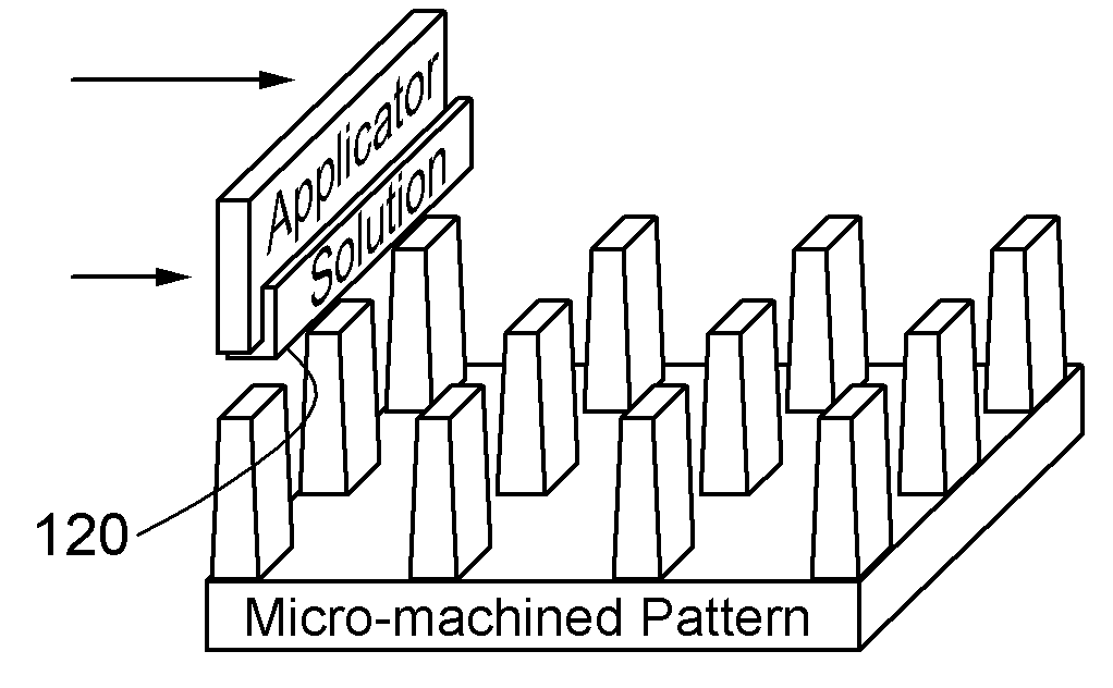
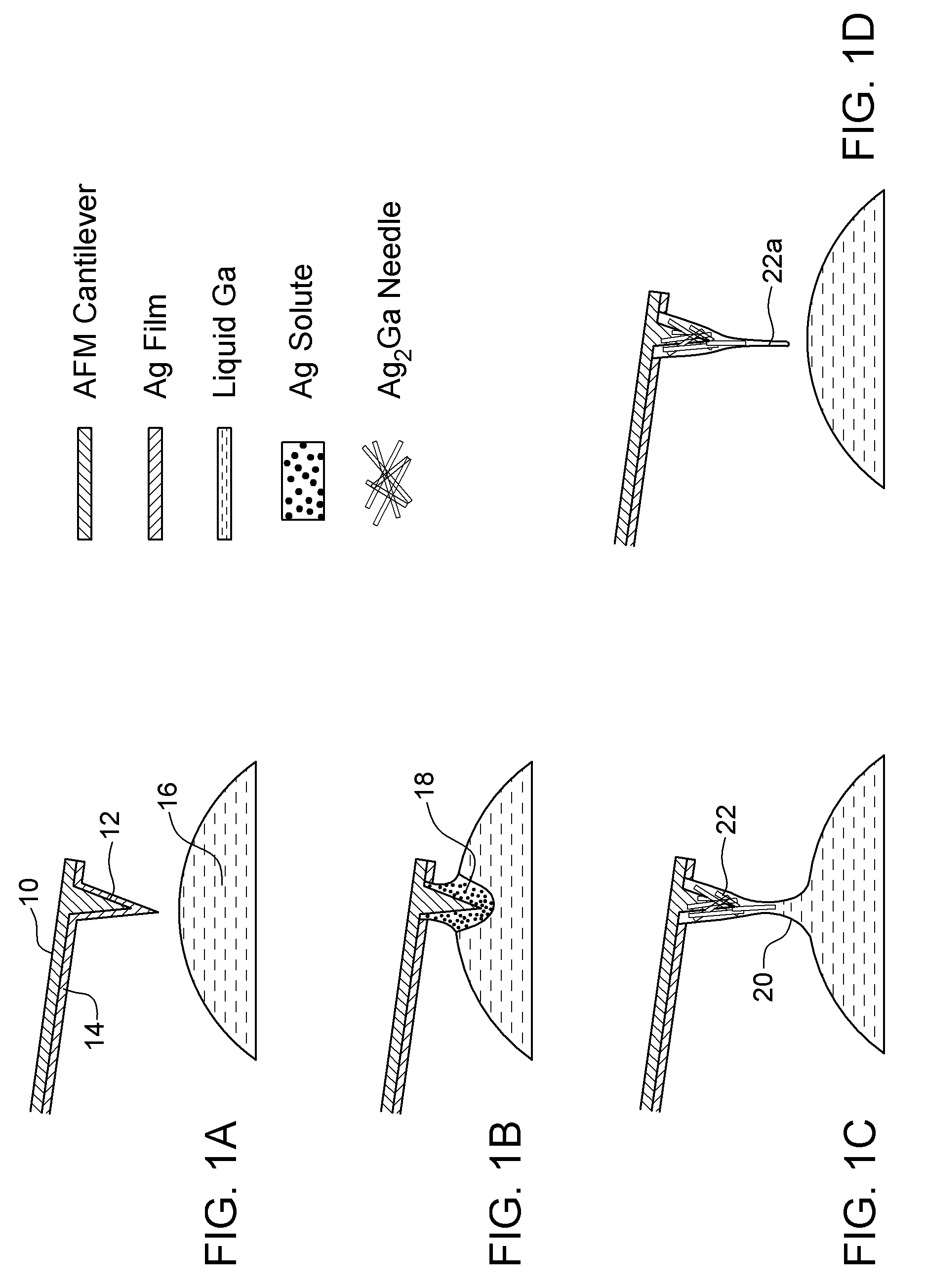
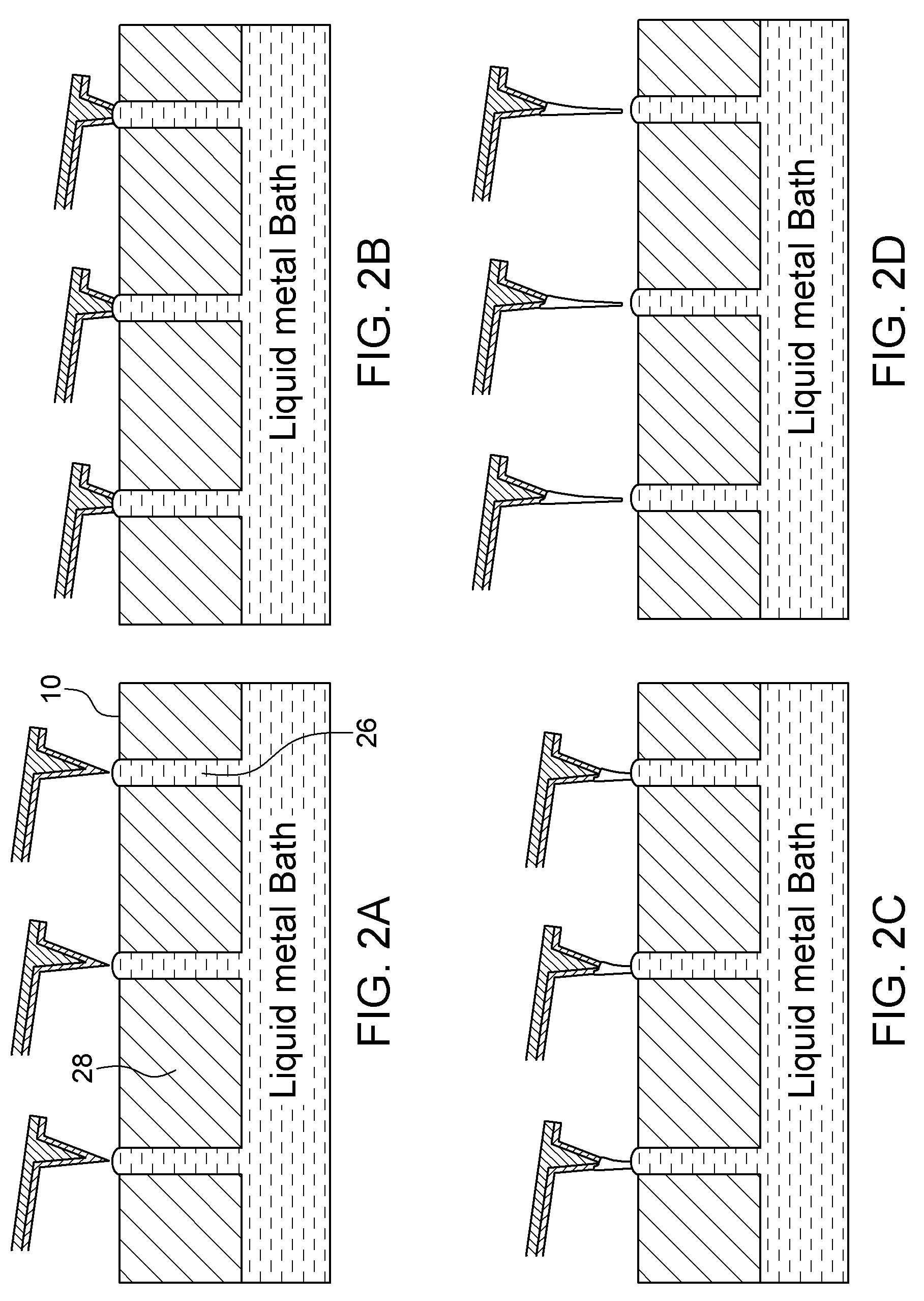
- The method involves self-assembly of metallic nanostructures, such as nanoneedles, using room temperature liquid metal droplets and controlled manipulation to form arrays of nanostructures with specific orientations and shapes, including coated and functionalized nanoneedles that can be used for various testing and measurement applications.

Safety Standards for Metal Nanomaterial Research
The establishment of comprehensive safety standards for metal nanomaterial research has become increasingly critical as the field of nanostructure integration advances. Current regulatory frameworks primarily draw from traditional chemical safety protocols, yet the unique properties of metal nanoparticles necessitate specialized approaches that address their distinct behavioral characteristics at the nanoscale.
International organizations including ISO, OECD, and NIOSH have developed preliminary guidelines specifically targeting nanomaterial handling procedures. These standards emphasize the importance of exposure assessment protocols, particularly for airborne nanoparticles that pose inhalation risks during synthesis and processing operations. The guidelines mandate the use of engineered controls such as fume hoods with HEPA filtration systems and negative pressure environments to minimize researcher exposure.
Personal protective equipment requirements for metal nanomaterial research extend beyond conventional laboratory safety measures. Specialized respirators with P100 filters, chemical-resistant gloves with extended cuff protection, and disposable laboratory coats are considered minimum requirements. Eye protection must include side shields to prevent particle contact, while closed-toe shoes with chemical resistance are mandatory in all nanomaterial handling areas.
Waste management protocols represent a particularly complex aspect of safety standardization. Metal nanoparticles cannot be disposed of through standard laboratory waste streams due to their potential environmental persistence and unknown long-term effects. Current standards require segregated collection systems, specialized labeling procedures, and coordination with certified hazardous waste disposal facilities equipped to handle nanoscale materials.
Facility design standards emphasize containment and monitoring capabilities. Laboratory spaces must incorporate continuous air monitoring systems capable of detecting nanoparticle concentrations, emergency shower and eyewash stations positioned within immediate reach of work areas, and specialized ventilation systems that prevent cross-contamination between research zones.
Training and certification requirements mandate that all personnel complete nanomaterial-specific safety courses before handling metal nanostructures. These programs cover risk assessment methodologies, emergency response procedures, and proper decontamination techniques. Regular refresher training ensures continued compliance with evolving safety protocols as new research reveals additional risk factors associated with various metal nanomaterial types.
Reproducibility Crisis in Nanostructure Experiments
The reproducibility crisis in nanostructure experiments has emerged as one of the most pressing challenges facing the field of metal nanostructure integration. This crisis stems from the inherent complexity of nanoscale systems, where minor variations in experimental conditions can lead to dramatically different outcomes. The problem is particularly acute in metal nanostructure research due to the sensitivity of metallic properties to surface conditions, oxidation states, and interfacial interactions.
Statistical analyses of published nanostructure studies reveal alarming trends in experimental reproducibility. Recent meta-analyses indicate that fewer than 40% of metal nanostructure synthesis protocols can be successfully replicated across different laboratories when following published methodologies. This low reproducibility rate significantly undermines the credibility of research findings and impedes the translation of laboratory discoveries into practical applications.
The root causes of this reproducibility crisis are multifaceted and interconnected. Environmental factors such as humidity, temperature fluctuations, and trace contaminants play crucial roles in determining experimental outcomes. Laboratory-to-laboratory variations in equipment calibration, reagent purity, and operator technique further compound these challenges. Additionally, the lack of standardized characterization protocols makes it difficult to compare results across different research groups.
Publication bias exacerbates the reproducibility problem by favoring positive results while discouraging the reporting of negative or inconclusive findings. This selective reporting creates a distorted view of experimental success rates and prevents the scientific community from learning from failed attempts. The pressure to publish novel results often leads researchers to inadequately document experimental details or overlook critical variables that influence reproducibility.
The consequences of poor reproducibility extend beyond academic concerns to impact industrial development and regulatory approval processes. Companies investing in nanostructure-based technologies face significant risks when scaling up processes based on irreproducible research. Regulatory agencies struggle to establish safety guidelines without consistent and reliable experimental data, potentially delaying the commercialization of beneficial technologies.
Addressing this crisis requires systematic reforms in experimental design, documentation standards, and publication practices. The development of standardized protocols, improved characterization methods, and collaborative validation studies represents essential steps toward restoring confidence in nanostructure research and enabling reliable technological advancement.
Unlock deeper insights with PatSnap Eureka Quick Research — get a full tech report to explore trends and direct your research. Try now!
Generate Your Research Report Instantly with AI Agent
Supercharge your innovation with PatSnap Eureka AI Agent Platform!