

How to Control Microstructure in Electron Beam Processes
MAR 18, 20269 MIN READ
Generate Your Research Report Instantly with AI Agent
PatSnap Eureka helps you evaluate technical feasibility & market potential.
Electron Beam Microstructure Control Background and Objectives
Electron beam processing has emerged as a transformative manufacturing technology since its initial development in the 1950s, evolving from basic welding applications to sophisticated additive manufacturing and surface modification techniques. The technology leverages high-energy electron beams to precisely manipulate materials at the microscopic level, enabling unprecedented control over material properties and structural characteristics.
The historical progression of electron beam technology demonstrates a clear trajectory from simple thermal processing to complex microstructural engineering. Early applications focused primarily on joining and melting operations, where the primary concern was achieving adequate penetration and fusion. However, as understanding of beam-material interactions deepened, researchers recognized the potential for controlling solidification patterns, grain structures, and phase distributions through precise manipulation of process parameters.
Contemporary electron beam processes encompass a diverse range of applications including additive manufacturing, surface alloying, powder bed fusion, and directed energy deposition. Each application presents unique challenges in microstructural control, requiring tailored approaches to beam management, thermal cycling, and material handling. The vacuum environment inherent to electron beam processing provides distinct advantages for controlling atmospheric contamination while presenting specific challenges for heat dissipation and material behavior.
The primary objective of microstructural control in electron beam processes centers on achieving predictable and repeatable material properties through systematic manipulation of processing parameters. This involves establishing correlations between beam characteristics, scanning strategies, thermal gradients, and resulting microstructural features such as grain size, phase distribution, and defect formation.
Critical technical goals include developing robust process windows that ensure consistent microstructural outcomes across varying geometries and material compositions. This requires comprehensive understanding of solidification dynamics, thermal history effects, and the complex interactions between multiple physical phenomena occurring simultaneously during processing.
Advanced objectives extend toward real-time microstructural monitoring and adaptive process control, enabling dynamic adjustment of processing parameters based on in-situ feedback. This represents a paradigm shift from static process optimization toward intelligent manufacturing systems capable of maintaining desired microstructural characteristics despite variations in material properties, environmental conditions, or geometric constraints.
The ultimate vision encompasses fully predictive microstructural design, where desired material properties can be directly translated into specific processing protocols, enabling unprecedented customization of material characteristics for specialized applications across aerospace, medical, and advanced manufacturing sectors.
Market Demand for Advanced Electron Beam Manufacturing
The global market for advanced electron beam manufacturing technologies is experiencing unprecedented growth driven by increasing demands for precision manufacturing across multiple high-value industries. Aerospace and defense sectors represent the largest market segment, where electron beam welding and additive manufacturing enable the production of critical components with superior mechanical properties and minimal thermal distortion. The ability to control microstructure through precise electron beam parameters has become essential for manufacturing turbine blades, structural components, and propulsion systems that meet stringent performance requirements.
Automotive industry transformation toward electric vehicles has created substantial demand for electron beam processing capabilities. Battery manufacturing requires precise welding of dissimilar materials, while lightweight structural components benefit from the controlled microstructural properties achievable through electron beam techniques. The semiconductor industry continues to drive demand for electron beam lithography and processing equipment, where nanoscale microstructure control directly impacts device performance and yield rates.
Medical device manufacturing represents a rapidly expanding market segment, particularly for implantable devices and surgical instruments. The biocompatibility and fatigue resistance of titanium alloys and other medical materials depend heavily on microstructural characteristics that can be precisely controlled through electron beam processing. Regulatory requirements for medical devices further emphasize the importance of consistent and controllable manufacturing processes.
Energy sector applications, including nuclear power components and renewable energy systems, require materials with exceptional reliability and longevity. Electron beam welding and surface modification techniques enable the production of components with tailored microstructures that enhance corrosion resistance, mechanical strength, and operational lifetime. The growing focus on clean energy infrastructure is expected to drive continued market expansion.
Market growth is further accelerated by increasing adoption of additive manufacturing technologies, where electron beam melting processes offer superior control over part density, grain structure, and mechanical properties compared to alternative methods. Industries are recognizing that microstructure control capabilities translate directly into improved product performance, reduced manufacturing defects, and enhanced operational reliability, creating strong economic incentives for technology adoption.
Current State and Challenges in EB Microstructure Control
Electron beam (EB) processes have emerged as critical manufacturing technologies across aerospace, automotive, and medical device industries, yet achieving precise microstructure control remains a formidable challenge. Current EB welding, melting, and additive manufacturing techniques struggle with inherent process complexities that directly impact final material properties and component performance.
The fundamental challenge lies in the rapid thermal cycles characteristic of EB processes. Heating rates can exceed 10^6 K/s, followed by equally rapid cooling, creating non-equilibrium conditions that are difficult to predict and control. This thermal volatility leads to heterogeneous microstructures with varying grain sizes, phase distributions, and residual stress patterns within single components.
Beam parameter optimization represents another significant hurdle. The interdependent relationships between beam power, scanning speed, focus position, and beam oscillation patterns create a multi-dimensional control space that is challenging to navigate systematically. Small variations in these parameters can result in dramatically different microstructural outcomes, making process repeatability difficult to achieve.
Material-specific challenges further complicate microstructure control. Different alloy systems respond uniquely to EB processing conditions, requiring tailored approaches for each material class. Titanium alloys, for instance, exhibit different phase transformation kinetics compared to nickel-based superalloys, necessitating distinct control strategies for optimal microstructure development.
Real-time monitoring and feedback control capabilities remain technologically immature. Current EB systems lack sophisticated in-situ characterization tools that could enable dynamic process adjustments based on evolving microstructural conditions. This limitation forces reliance on post-process analysis and iterative parameter refinement, significantly extending development cycles.
Computational modeling tools, while advancing rapidly, still struggle to accurately predict microstructural evolution under the extreme conditions present in EB processes. The coupling of thermal, mechanical, and metallurgical phenomena across multiple length and time scales presents computational challenges that current simulation capabilities cannot fully address.
Scale-up from laboratory to production environments introduces additional complexities. Microstructure control strategies developed for small-scale specimens often fail when applied to larger components due to thermal management differences and beam interaction variations across extended processing volumes.
Existing Solutions for EB Microstructure Management
01 Electron beam irradiation for surface modification and microstructure control
Electron beam processes can be used to modify surface properties and control microstructure of materials through precise energy delivery. The technique allows for localized heating and rapid cooling, enabling the formation of specific microstructural features such as refined grain structures, improved surface hardness, and enhanced wear resistance. This process is particularly effective for treating metallic materials and alloys to achieve desired mechanical properties.- Electron beam irradiation for material surface modification: Electron beam processes can be used to modify the surface microstructure of materials by controlled irradiation. This technique allows for precise control of penetration depth and energy deposition, resulting in altered surface properties such as hardness, wear resistance, and corrosion resistance. The process can create refined grain structures and improved surface characteristics without affecting the bulk material properties.
- Electron beam welding and joining techniques: Electron beam technology enables high-precision welding and joining of materials with minimal heat-affected zones. The focused beam creates narrow, deep welds with fine microstructural features. This process is particularly effective for joining dissimilar materials and creating strong bonds with controlled grain structures in the weld zone, resulting in superior mechanical properties compared to conventional welding methods.
- Microstructure refinement through electron beam melting: Electron beam melting processes can be utilized to refine microstructures in metallic materials through rapid heating and controlled cooling cycles. This technique produces fine-grained structures with improved mechanical properties. The process allows for layer-by-layer material processing, enabling the creation of complex geometries with tailored microstructural characteristics throughout the component.
- Electron beam treatment for semiconductor and thin film applications: Electron beam processes are employed in semiconductor manufacturing and thin film deposition to create specific microstructural features at the nanoscale. The technique enables precise control of crystallinity, grain size, and defect density in thin films. This approach is valuable for producing electronic devices with enhanced performance characteristics through controlled microstructural engineering.
- Electron beam curing and polymerization processes: Electron beam radiation can initiate and control polymerization reactions, creating specific microstructures in polymer materials and coatings. This process offers advantages in terms of processing speed, depth of cure, and the ability to create crosslinked networks with controlled morphology. The technique is applicable to various coating and composite material applications where specific microstructural properties are desired.
02 Electron beam welding and joining with controlled microstructure
Electron beam welding processes enable precise joining of materials while maintaining control over the resulting microstructure in the weld zone and heat-affected areas. The high energy density and focused beam characteristics allow for deep penetration welding with minimal thermal distortion. The process parameters can be optimized to achieve specific microstructural characteristics such as fine grain size, reduced porosity, and improved mechanical properties in the joint region.Expand Specific Solutions03 Electron beam melting for additive manufacturing microstructure
Electron beam melting technology is utilized in additive manufacturing to create components with controlled microstructures layer by layer. The process involves selective melting of powder materials using an electron beam, allowing for precise control over solidification rates and thermal gradients. This enables the production of parts with tailored microstructural features including grain orientation, phase distribution, and density, which directly influence the mechanical properties of the final product.Expand Specific Solutions04 Electron beam treatment for semiconductor and thin film microstructure
Electron beam processes are employed to modify and control microstructures in semiconductor materials and thin films. The technique enables precise annealing, crystallization, and doping processes at localized areas without affecting surrounding regions. This approach is valuable for creating specific microstructural features in electronic devices, including controlled grain boundaries, phase transformations, and defect engineering to optimize electrical and optical properties.Expand Specific Solutions05 Electron beam curing and cross-linking for polymer microstructure
Electron beam radiation is used to induce curing and cross-linking in polymer materials, resulting in controlled microstructural changes. The process enables rapid polymerization and network formation without the need for thermal heating or chemical initiators. This technique allows for precise control over the degree of cross-linking, crystallinity, and molecular architecture, leading to enhanced mechanical strength, thermal stability, and chemical resistance in the treated polymer materials.Expand Specific Solutions
Key Players in Electron Beam Equipment and Services
The electron beam microstructure control technology represents a mature industrial sector experiencing steady growth, driven by increasing demand for precision manufacturing in semiconductors and advanced materials. The market demonstrates significant scale with established players like Applied Materials, Hitachi, and Toshiba leading commercial applications, while specialized firms such as NuFlare Technology and Canon Anelva focus on niche electron beam solutions. Technology maturity varies across applications, with semiconductor manufacturing showing high sophistication through companies like ICT Integrated Circuit Testing and Carl Zeiss MultiSEM, while emerging applications in additive manufacturing and materials processing remain in development phases. The competitive landscape includes strong academic-industry collaboration, evidenced by research institutions like University of Tokyo, Columbia University, and various Chinese universities working alongside industrial partners, indicating robust innovation pipelines for next-generation microstructure control techniques.
NuFlare Technology, Inc.
Technical Solution: NuFlare Technology specializes in electron beam lithography systems with sophisticated microstructure control mechanisms for advanced semiconductor device fabrication. Their multi-beam mask writer systems employ precise beam current control and advanced blanking systems to achieve uniform exposure patterns that directly influence microstructural development in photoresist and underlying materials. The company's technology features real-time beam monitoring and correction systems that maintain consistent beam characteristics throughout the exposure process. Their electron beam systems incorporate advanced stage control with interferometric positioning feedback and environmental isolation to minimize vibrations and thermal effects that could compromise microstructural precision. NuFlare's proprietary dose control algorithms optimize exposure parameters to achieve desired grain structures and material properties in thin films and nanostructures.
Strengths: Specialized expertise in multi-beam systems, excellent beam stability and uniformity, advanced dose control algorithms. Weaknesses: Primarily focused on lithography applications, limited broader materials processing capabilities, high system complexity requiring specialized expertise.
Hitachi Ltd.
Technical Solution: Hitachi has developed sophisticated electron beam systems with advanced microstructure control capabilities, particularly for their electron beam lithography and inspection equipment. Their technology employs variable-shaped beam systems that can dynamically adjust beam geometry and intensity distribution to control material deposition patterns and crystalline structure formation. The company's electron beam systems integrate thermal management solutions and real-time process monitoring to maintain consistent microstructural properties during processing. Their proprietary beam shaping technology allows for precise control of energy density distribution, enabling tailored microstructure development in various materials including metals, semiconductors, and ceramics. Hitachi's systems also incorporate machine learning algorithms to predict and compensate for process variations that could affect microstructural uniformity.
Strengths: Advanced beam shaping technology, strong integration of AI/ML for process optimization, comprehensive thermal management systems. Weaknesses: Higher complexity in system operation, significant capital investment requirements, limited customization options for specialized applications.
Core Innovations in Electron Beam Parameter Control
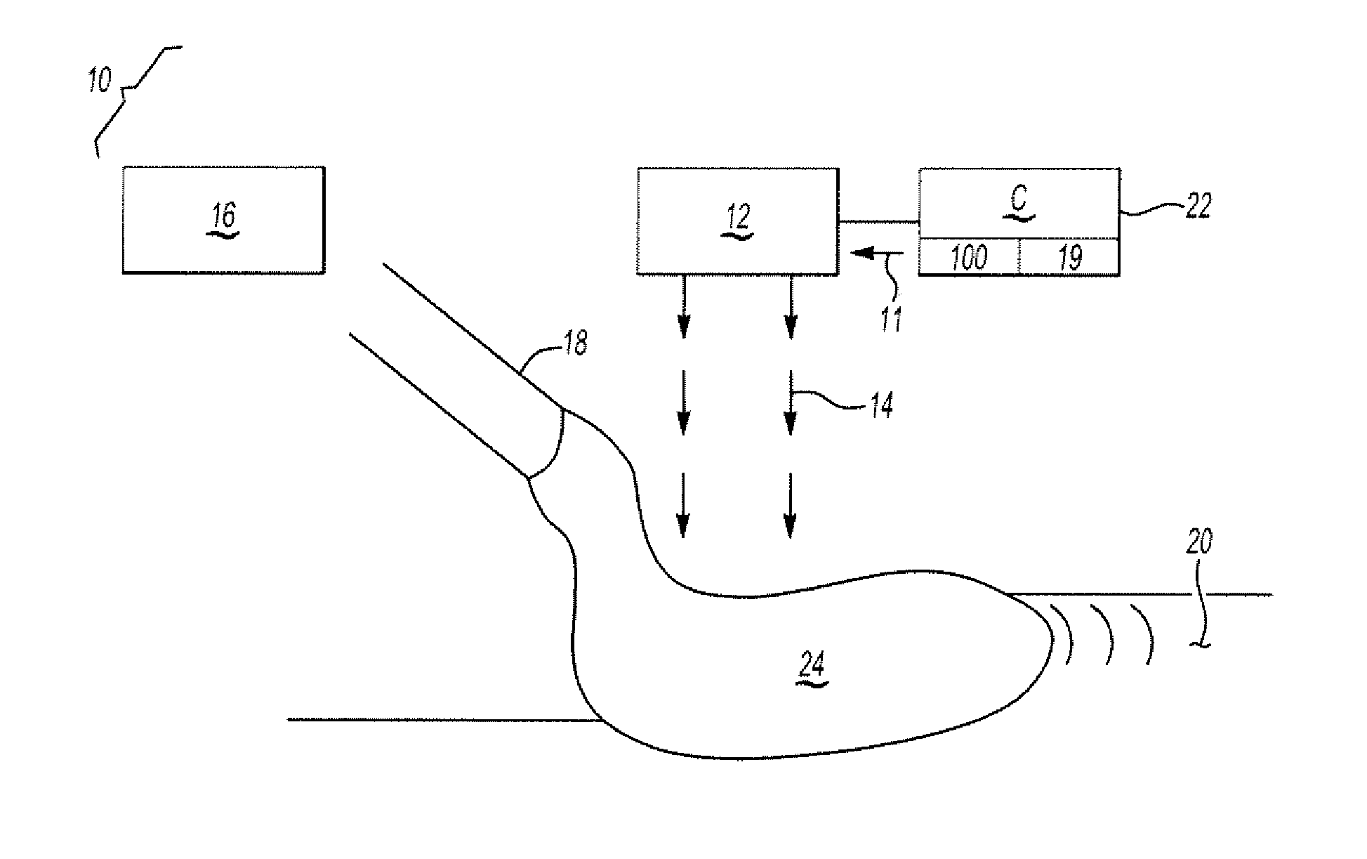
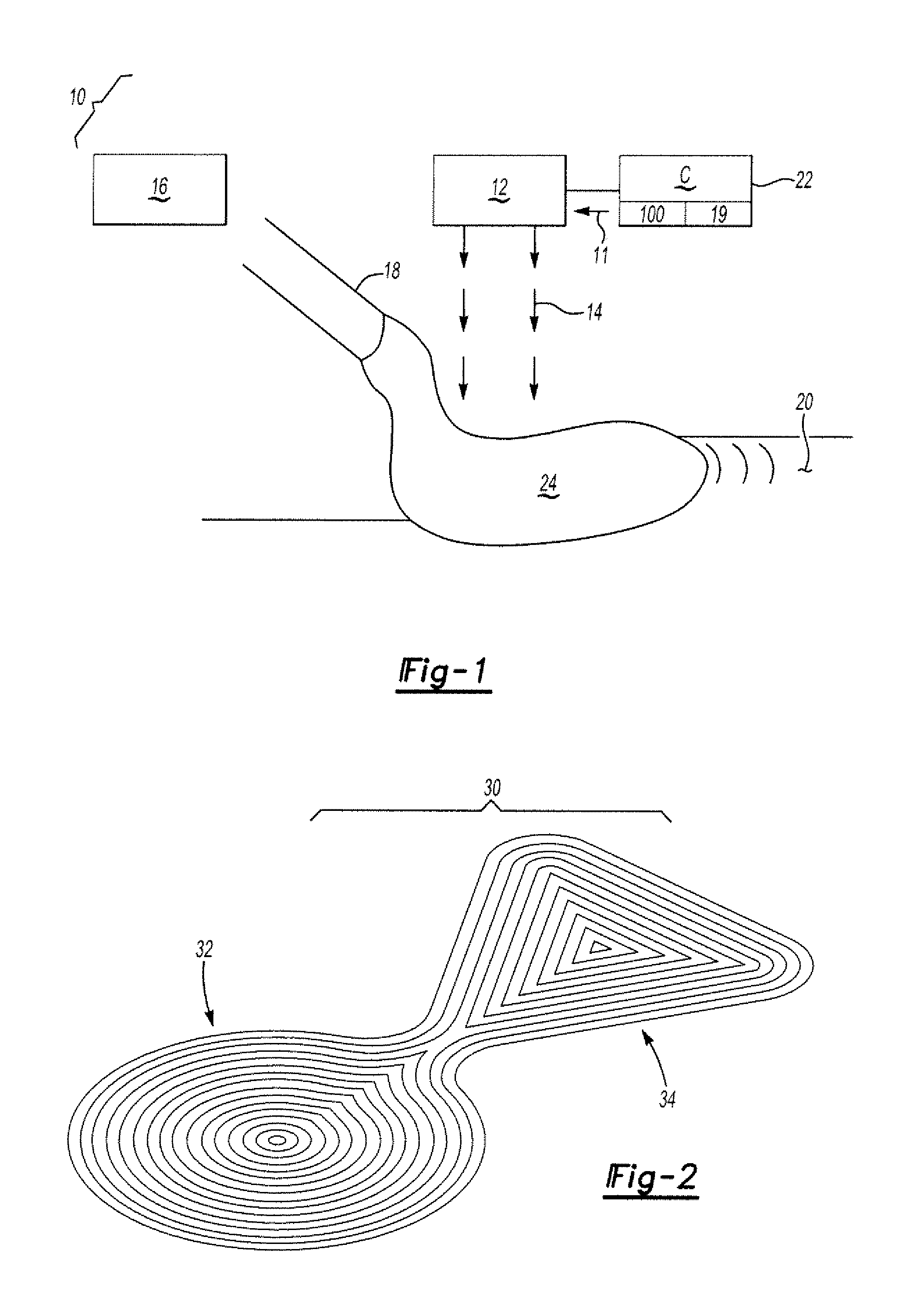
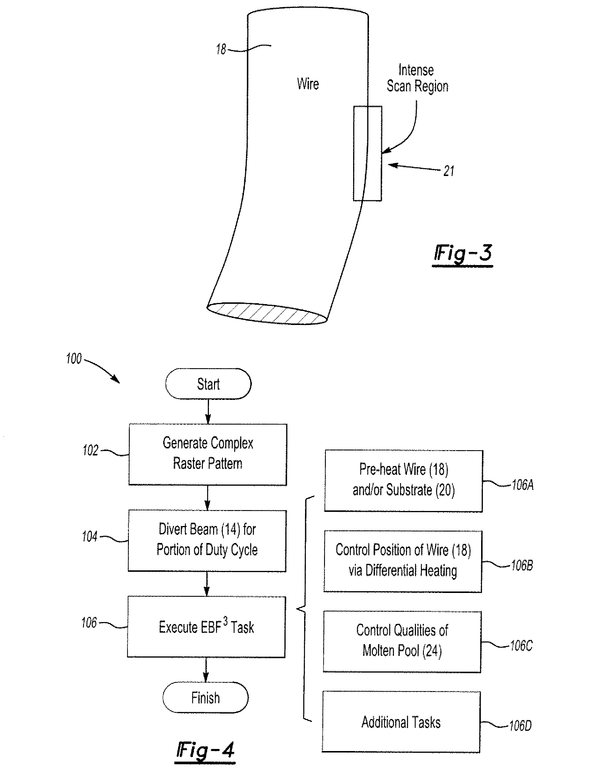
Use of beam deflection to control an electron beam wire deposition process
PatentInactiveUS8344281B2
Innovation
- A method and apparatus that utilize a complex raster pattern for the electron beam to steer and preheat the wire, allowing for simultaneous multi-task processing, self-correction of the wire position, and optimized thermal input, reducing flaws by focusing the beam on the wire's outer edges to maintain it within the molten pool.
Method for modification of surfaces of metallic materials using electron beam
PatentInactiveEP2727679A1
Innovation
- The method employs a controlled electron beam in a vacuum chamber to create macro- and microstructures by selectively melting and re-depositing material, combining regular and stochastic structures through complex beam pulsing, deflection, focusing, and relative movement, allowing for the simultaneous formation of both macro- and microstructures with specific sizes and geometries.


Safety Standards for High-Energy Electron Beam Operations
High-energy electron beam operations present significant safety challenges that require comprehensive regulatory frameworks and standardized protocols. The inherent risks associated with electron beam processing, including radiation exposure, electrical hazards, and material interactions, necessitate stringent safety measures to protect personnel and equipment while maintaining operational efficiency.
International safety standards for electron beam operations are primarily governed by organizations such as the International Electrotechnical Commission (IEC), the International Atomic Energy Agency (IAEA), and national regulatory bodies like the Nuclear Regulatory Commission (NRC) in the United States. IEC 60601-2-1 provides fundamental safety requirements for electron beam equipment, while IAEA Safety Standards Series establishes guidelines for radiation protection in industrial applications. These standards define maximum permissible exposure limits, typically maintaining radiation levels below 2 mSv per year for occupational workers in controlled areas.
Personnel protection protocols encompass multiple layers of safety measures, including administrative controls, engineering safeguards, and personal protective equipment. Access control systems must implement fail-safe mechanisms that automatically shut down beam operations when unauthorized entry is detected. Radiation monitoring systems require real-time dosimetry with alarm thresholds set at predetermined levels, typically 10% of annual dose limits for immediate response protocols.
Equipment safety standards mandate comprehensive shielding designs that account for both primary beam radiation and secondary X-ray generation. Shielding calculations must consider beam energy levels, with high-energy operations above 10 MeV requiring specialized concrete or lead barriers. Interlock systems must demonstrate triple redundancy for critical safety functions, ensuring beam termination within milliseconds of safety system activation.
Emergency response procedures require detailed protocols for radiation incidents, equipment malfunctions, and personnel exposure scenarios. Training programs must include annual certification requirements for operators, with specialized qualifications for high-energy systems exceeding 5 MeV. Regular safety audits and compliance assessments ensure adherence to evolving regulatory requirements and technological advancements in electron beam safety systems.
Quality Assurance in Electron Beam Manufacturing
Quality assurance in electron beam manufacturing represents a critical framework for ensuring consistent microstructural control and product reliability. The implementation of comprehensive QA protocols directly impacts the ability to achieve desired material properties and dimensional accuracy in electron beam processed components. Modern QA systems integrate real-time monitoring capabilities with post-process validation techniques to maintain stringent quality standards throughout the manufacturing cycle.
Real-time process monitoring forms the foundation of effective quality assurance in electron beam operations. Advanced sensor networks continuously track critical parameters including beam current stability, vacuum levels, substrate temperature, and powder feed rates during processing. These monitoring systems employ sophisticated algorithms to detect deviations from optimal processing windows and trigger immediate corrective actions. Statistical process control methodologies are integrated to establish control limits and identify trends that may indicate potential quality issues before they manifest in final products.
Non-destructive testing techniques play an essential role in validating microstructural integrity without compromising component functionality. X-ray computed tomography enables detailed internal defect detection, while ultrasonic testing identifies subsurface discontinuities that could affect mechanical performance. Electron backscatter diffraction provides crystallographic information to verify grain structure alignment with design specifications. These techniques collectively ensure that manufactured components meet stringent aerospace and medical device standards.
Dimensional metrology systems complement microstructural assessments by verifying geometric accuracy and surface finish quality. Coordinate measuring machines equipped with high-resolution probes capture precise dimensional data, while optical profilometry quantifies surface roughness parameters. Integration of these measurement systems with manufacturing execution systems enables automated pass/fail decisions and facilitates continuous process optimization based on quality feedback loops.
Certification protocols establish traceability requirements and documentation standards essential for regulated industries. Material certification includes chemical composition verification, mechanical property validation, and microstructural characterization reports. Process certification encompasses equipment qualification, operator training records, and environmental condition monitoring. These comprehensive documentation systems ensure regulatory compliance while providing valuable data for continuous improvement initiatives and failure analysis investigations when quality issues arise.
Unlock deeper insights with PatSnap Eureka Quick Research — get a full tech report to explore trends and direct your research. Try now!
Generate Your Research Report Instantly with AI Agent
Supercharge your innovation with PatSnap Eureka AI Agent Platform!