

How To Optimize Pulse Time In Atomic Layer Deposition Reactions
MAY 13, 20269 MIN READ
Generate Your Research Report Instantly with AI Agent
PatSnap Eureka helps you evaluate technical feasibility & market potential.
ALD Pulse Timing Background and Optimization Goals
Atomic Layer Deposition (ALD) has emerged as a critical thin film deposition technique since its commercial introduction in the 1970s, initially developed for manufacturing electroluminescent displays. The technology gained significant momentum in the semiconductor industry during the 1990s as device dimensions continued to shrink, demanding unprecedented precision in film thickness control and conformality. ALD's unique self-limiting surface chemistry enables atomic-scale control over film growth, making it indispensable for advanced semiconductor manufacturing, energy storage devices, and emerging nanotechnology applications.
The fundamental principle of ALD relies on sequential, self-terminating surface reactions that occur through carefully timed precursor pulses. Each ALD cycle consists of alternating exposures to different chemical precursors, separated by purge steps to remove unreacted species and reaction byproducts. The temporal control of these pulses directly influences reaction completeness, film quality, and overall process efficiency. However, determining optimal pulse timing remains one of the most challenging aspects of ALD process development, as it requires balancing multiple competing factors.
Current ALD processes face significant challenges in pulse timing optimization due to the complex interplay between precursor transport, surface kinetics, and reactor design. Insufficient pulse duration can lead to incomplete surface coverage and non-uniform film growth, while excessive pulse times result in precursor waste, extended cycle times, and potential parasitic reactions. The situation becomes more complex when considering high-aspect-ratio structures, where precursor transport limitations can create significant timing requirements variations across different feature geometries.
The primary optimization goal centers on achieving complete monolayer formation with minimal cycle time while maintaining excellent film uniformity and conformality. This requires establishing the minimum pulse duration necessary for full surface saturation under specific process conditions, including temperature, pressure, and substrate geometry. Additionally, optimizing purge times between precursor pulses is crucial to prevent cross-contamination and unwanted gas-phase reactions that can compromise film quality.
Advanced optimization objectives extend beyond basic timing parameters to encompass dynamic pulse strategies that adapt to changing surface conditions throughout the deposition process. These include developing predictive models for pulse timing based on real-time process monitoring, implementing gradient pulse sequences for complex three-dimensional structures, and establishing robust timing protocols that maintain performance across varying substrate types and process conditions. The ultimate goal is achieving maximum throughput while preserving the inherent advantages of atomic-scale precision that define ALD technology.
Market Demand for Enhanced ALD Process Efficiency
The semiconductor industry's relentless pursuit of smaller node geometries and advanced device architectures has created unprecedented demand for enhanced atomic layer deposition process efficiency. As manufacturers transition to sub-5nm processes and explore three-dimensional device structures, the precision and throughput requirements for ALD systems have intensified dramatically. The industry faces mounting pressure to reduce manufacturing costs while maintaining the atomic-scale precision that ALD uniquely provides.
Memory manufacturers, particularly those producing 3D NAND flash devices with layer counts exceeding 200 levels, represent the largest consumer segment driving ALD efficiency improvements. These applications require hundreds of ALD cycles per device, making process optimization critical for economic viability. The transition from planar to vertical device architectures has exponentially increased the total ALD processing time per wafer, creating bottlenecks in high-volume manufacturing environments.
Logic device manufacturers face similar challenges as they implement advanced gate-all-around transistor architectures and explore new materials for next-generation nodes. The complexity of these structures demands multiple ALD processes with different precursor chemistries, each requiring optimized pulse timing parameters. Foundries report that ALD processes now constitute a significant portion of total wafer processing time, directly impacting fab utilization rates and manufacturing economics.
The emerging markets for compound semiconductors, power electronics, and photonic devices are creating additional demand vectors for efficient ALD processes. These applications often require specialized material systems and non-standard substrate sizes, necessitating flexible process optimization capabilities. The automotive semiconductor sector's growth, driven by electrification and autonomous driving technologies, has further amplified the need for cost-effective ALD solutions.
Equipment manufacturers face increasing pressure from fab operators to deliver systems with higher throughput capabilities without compromising film quality or uniformity. The industry's shift toward larger wafer sizes and batch processing systems has created opportunities for process optimization through advanced pulse timing strategies. Market dynamics indicate that ALD system suppliers who can demonstrate significant throughput improvements while maintaining process control will capture disproportionate market share in the expanding ALD equipment market.
Current ALD Pulse Time Challenges and Limitations
Atomic Layer Deposition processes face significant challenges in optimizing pulse timing parameters, which directly impact film quality, deposition uniformity, and manufacturing efficiency. Current ALD systems struggle with determining optimal precursor pulse durations across different substrate materials and reactor configurations, leading to suboptimal process conditions that compromise both throughput and film properties.
One of the primary limitations lies in the lack of real-time monitoring capabilities for surface saturation during precursor exposure. Traditional ALD processes rely on predetermined pulse times based on empirical testing, which often results in either insufficient surface coverage or excessive precursor waste. This approach becomes particularly problematic when dealing with high aspect ratio structures or complex three-dimensional geometries where mass transport limitations significantly affect precursor delivery and surface reaction kinetics.
Temperature-dependent reaction kinetics present another critical challenge in pulse time optimization. At lower processing temperatures, slower surface reaction rates require extended pulse durations to achieve complete monolayer formation, while higher temperatures may lead to precursor decomposition or unwanted gas-phase reactions if pulse times are not carefully controlled. The narrow processing windows for many ALD chemistries make it difficult to establish universal pulse timing protocols.
Substrate-dependent variations further complicate pulse time optimization efforts. Different surface chemistries, roughness levels, and thermal properties require tailored pulse parameters, making it challenging to develop standardized processes for multi-material applications. The initial nucleation behavior on various substrates can vary dramatically, necessitating adaptive pulse timing strategies that current ALD systems cannot readily accommodate.
Purge time optimization represents an equally complex challenge, as insufficient purging can lead to chemical vapor deposition-like reactions and non-uniform film growth, while excessive purge times reduce overall process efficiency. The interdependence between pulse and purge timing parameters creates a multidimensional optimization problem that is difficult to solve using conventional approaches.
Scale-up limitations from laboratory to production environments introduce additional complications, as reactor design differences, gas flow dynamics, and thermal uniformity variations all influence optimal pulse timing requirements. These factors often necessitate complete reoptimization of pulse parameters when transitioning from research to manufacturing scales.
Existing ALD Pulse Time Optimization Solutions
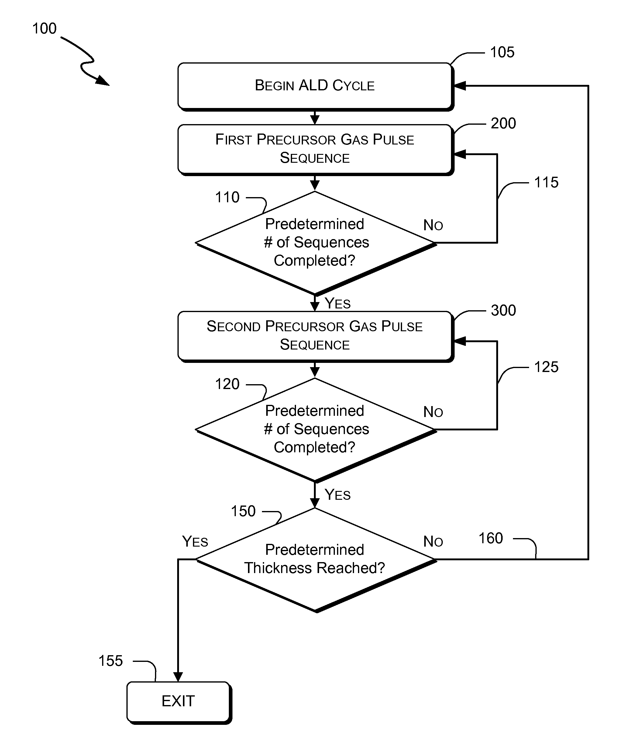
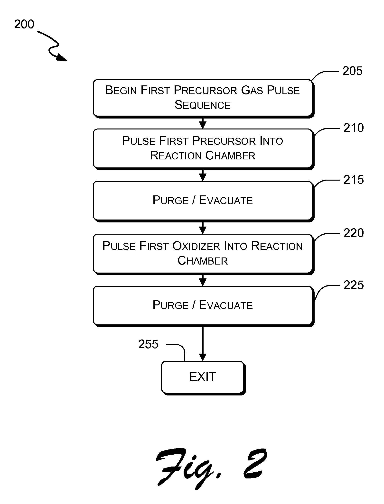
01 Optimization of precursor pulse duration for uniform deposition
The duration of precursor pulses in atomic layer deposition processes can be optimized to achieve uniform film thickness and coverage. Proper pulse timing ensures complete surface saturation while minimizing material waste and process time. The pulse duration must be carefully controlled to allow sufficient time for precursor molecules to reach all surface sites, particularly in high aspect ratio structures.- Optimization of precursor pulse duration for uniform deposition: The duration of precursor pulses in atomic layer deposition processes can be optimized to achieve uniform film thickness and coverage. Proper pulse timing ensures complete surface saturation while minimizing waste of precursor materials. The pulse duration must be sufficient to allow precursor molecules to reach all surface sites, particularly in high aspect ratio structures, while avoiding excessive exposure that could lead to multilayer adsorption or gas phase reactions.
- Purge time control between precursor and reactant pulses: The purge time between different precursor pulses is critical for removing unreacted species and preventing gas phase reactions. Adequate purge duration ensures that only surface-adsorbed species remain before the next pulse, maintaining the self-limiting nature of the deposition process. The purge time must be optimized based on reactor geometry, pumping speed, and precursor volatility to achieve high-quality films with precise thickness control.
- Temperature-dependent pulse timing optimization: Pulse timing parameters must be adjusted according to deposition temperature to maintain optimal reaction kinetics and surface chemistry. Higher temperatures typically allow for shorter pulse times due to increased reaction rates and precursor mobility, while lower temperatures may require extended pulse durations to achieve complete surface reactions. Temperature-dependent optimization ensures consistent film quality across different thermal processing conditions.
- Substrate-specific pulse sequence design: Different substrate materials and surface morphologies require customized pulse timing sequences to achieve optimal deposition results. The pulse parameters must account for substrate reactivity, surface area, and geometric complexity. Patterned substrates or three-dimensional structures may need longer pulse times to ensure complete precursor penetration and uniform coverage, while planar surfaces can utilize shorter, more efficient pulse sequences.
- Real-time pulse timing control and monitoring: Advanced control systems enable real-time adjustment of pulse timing parameters based on process monitoring and feedback mechanisms. These systems can detect incomplete reactions or non-uniform deposition and automatically adjust pulse durations to maintain process stability. Integration of sensors and control algorithms allows for dynamic optimization of pulse sequences during deposition, improving yield and reproducibility while reducing development time for new processes.
02 Purge time control between deposition cycles
The purge time between precursor and reactant pulses is critical for removing unreacted species and preventing gas phase reactions. Optimal purge timing ensures that only surface-bound species participate in the deposition reaction, maintaining the self-limiting nature of the process. Insufficient purge time can lead to contamination and non-uniform film properties.Expand Specific Solutions03 Temperature-dependent pulse timing optimization
Pulse timing parameters must be adjusted based on substrate temperature to account for changes in reaction kinetics and precursor adsorption rates. Higher temperatures typically require shorter pulse times due to increased reaction rates, while lower temperatures may need extended pulses for complete surface coverage. Temperature optimization helps achieve consistent film quality across different processing conditions.Expand Specific Solutions04 Substrate geometry influence on pulse parameters
The geometry and surface area of substrates significantly affect the required pulse timing for complete coverage. Complex three-dimensional structures and high aspect ratio features require longer pulse times to ensure precursor penetration and uniform deposition. Pulse parameters must be tailored to specific substrate configurations to maintain film uniformity and conformality.Expand Specific Solutions05 Real-time pulse timing control and monitoring
Advanced control systems enable real-time adjustment of pulse timing based on process feedback and monitoring data. These systems can automatically optimize pulse duration and frequency to maintain consistent deposition rates and film properties. Real-time control helps compensate for variations in chamber conditions and substrate characteristics during processing.Expand Specific Solutions
Key Players in ALD Equipment and Process Industry
The atomic layer deposition (ALD) pulse time optimization field represents a mature technology sector experiencing steady growth, driven by increasing demand for precise thin-film deposition in semiconductor manufacturing and emerging applications. The market demonstrates significant scale with established players like Applied Materials, ASM International, and Veeco Instruments leading equipment development, while major semiconductor manufacturers including Intel, Samsung Electronics, and TSMC drive adoption through advanced node requirements. Technology maturity varies across segments, with companies like NEXUSBE specializing in spatial ALD innovations and research institutions such as Zhejiang University and Huazhong University of Science & Technology advancing fundamental understanding. The competitive landscape shows consolidation among equipment suppliers, while process optimization remains critical for next-generation semiconductor devices, energy storage applications, and flexible electronics manufacturing.
Applied Materials, Inc.
Technical Solution: Applied Materials has developed advanced pulse timing optimization strategies for ALD processes, focusing on precursor saturation analysis and surface reaction kinetics modeling. Their approach involves real-time monitoring of precursor adsorption using in-situ spectroscopy to determine optimal pulse durations. The company employs machine learning algorithms to predict ideal pulse times based on substrate temperature, precursor vapor pressure, and chamber geometry. Their systems feature adaptive pulse control that automatically adjusts timing parameters during deposition to maintain consistent film quality and maximize throughput efficiency.
Strengths: Industry-leading equipment with comprehensive process control and extensive R&D capabilities. Weaknesses: High equipment costs and complex system integration requirements.
ASM International NV
Technical Solution: ASM International has pioneered dynamic pulse optimization techniques that utilize pressure decay analysis to determine precursor saturation points in real-time. Their methodology combines computational fluid dynamics modeling with experimental validation to establish optimal pulse durations for different precursor chemistries. The company's approach includes temperature-dependent pulse scheduling and multi-zone timing control for batch reactors. They have developed proprietary algorithms that correlate pulse timing with film conformality and step coverage, enabling precise control over deposition uniformity across complex 3D structures.
Strengths: Strong focus on batch processing efficiency and excellent technical expertise in ALD chemistry. Weaknesses: Limited market presence compared to larger competitors and higher per-wafer processing costs.
Core Innovations in ALD Pulse Timing Control
Methods for controlling pulse shape in ALD processes
PatentActiveUS20230366088A1
Innovation
- A variable flow valve is used to generate a predetermined flow pulse profile, controlling the gas flow to both inner and outer regions of the substrate support, ensuring consistent dosing and smoother transitions between gas pulses.


Atomic layer deposition of hafnium lanthanum oxides
PatentActiveUS8071452B2
Innovation
- The method involves using a combination of tetrakis-ethyl-methylamino hafnium (TEMAHf) and Lanthanum tris-formamidinate (LaFAMD)3 as precursors, with a controlled pulse sequence and oxidant mixture of oxygen and ozone, maintained at low temperatures to minimize crystallization and impurities, allowing for efficient deposition of HfLaO films with improved throughput.

Environmental Impact of ALD Process Efficiency
The environmental implications of ALD process efficiency optimization through pulse time control represent a critical intersection between manufacturing performance and sustainability objectives. Efficient pulse timing directly correlates with reduced material consumption, energy usage, and waste generation throughout the deposition process. When pulse durations are optimized, precursor utilization rates improve significantly, minimizing the release of unreacted chemicals into exhaust systems and reducing the overall environmental footprint of semiconductor manufacturing operations.
Energy consumption patterns in ALD systems demonstrate strong sensitivity to pulse timing parameters. Extended pulse durations often lead to unnecessary heating cycles and prolonged vacuum maintenance, resulting in elevated power consumption per deposited layer. Conversely, optimized pulse sequences can reduce total process time by 15-30%, directly translating to lower energy requirements and decreased carbon emissions from manufacturing facilities. This efficiency gain becomes particularly significant in high-volume production environments where cumulative energy savings can reach substantial levels.
Precursor waste reduction emerges as another crucial environmental benefit of pulse time optimization. Inefficient timing parameters typically result in excess precursor delivery, leading to increased chemical waste streams and higher disposal costs. Optimized pulse sequences ensure maximum precursor utilization efficiency, reducing both raw material consumption and hazardous waste generation. This optimization directly impacts the lifecycle environmental assessment of ALD processes, improving sustainability metrics across multiple categories.
The relationship between process efficiency and environmental compliance becomes increasingly important as regulatory frameworks tighten around semiconductor manufacturing emissions. Optimized ALD processes generate fewer volatile organic compounds and reduce the burden on facility air treatment systems. This improvement not only enhances environmental performance but also reduces operational costs associated with emission control equipment and regulatory compliance monitoring.
Long-term environmental benefits extend beyond immediate process improvements to include reduced facility infrastructure requirements. Efficient ALD processes require smaller exhaust treatment systems, reduced chemical storage capacity, and lower utility demands, contributing to overall facility sustainability goals and supporting corporate environmental responsibility initiatives.
Quality Control Standards for ALD Processes
Quality control standards for ALD processes represent a critical framework for ensuring consistent and reliable atomic layer deposition outcomes, particularly when optimizing pulse timing parameters. These standards encompass comprehensive measurement protocols, statistical process control methodologies, and acceptance criteria that directly impact pulse time optimization strategies.
The foundation of ALD quality control lies in establishing precise measurement standards for film thickness uniformity, typically requiring less than 2% variation across substrate surfaces. This uniformity directly correlates with pulse time optimization, as insufficient precursor exposure leads to incomplete surface coverage, while excessive pulse duration results in material waste without performance improvement. Industry standards mandate real-time monitoring of growth per cycle (GPC) values, which serve as immediate feedback for pulse time adjustments.
Temperature control standards constitute another essential component, requiring substrate temperature stability within ±1°C during deposition cycles. This thermal precision directly influences the kinetics of surface reactions and precursor adsorption rates, making it fundamental for determining optimal pulse durations. Quality control protocols specify continuous temperature monitoring at multiple substrate locations to ensure uniform reaction conditions.
Precursor delivery system standards focus on maintaining consistent flow rates and pressure stability throughout the deposition process. These parameters must remain within specified tolerances, typically ±2% for flow rates and ±0.1% for chamber pressure, to ensure reproducible pulse timing optimization results. Advanced quality control systems incorporate mass flow controller calibration schedules and automated pressure regulation feedback loops.
Statistical process control implementation requires establishing control charts for key process variables including pulse duration, purge times, and cycle-to-cycle repeatability metrics. These charts enable rapid identification of process drift and facilitate proactive adjustments to maintain optimal pulse timing parameters. Industry best practices recommend implementing Six Sigma methodologies with capability indices exceeding 1.33 for critical process parameters.
Contamination control standards mandate rigorous monitoring of residual precursor levels and by-product formation, as these factors significantly impact optimal pulse timing requirements. Quality control protocols specify maximum allowable contamination levels and require regular system purging procedures to maintain process integrity and ensure accurate pulse time optimization.
Unlock deeper insights with PatSnap Eureka Quick Research — get a full tech report to explore trends and direct your research. Try now!
Generate Your Research Report Instantly with AI Agent
Supercharge your innovation with PatSnap Eureka AI Agent Platform!