How To Reduce Interface Defects In Atomic Layer Deposition For Semiconductors
MAY 13, 20269 MIN READ
Generate Your Research Report Instantly with AI Agent
PatSnap Eureka helps you evaluate technical feasibility & market potential.
ALD Interface Defect Challenges and Semiconductor Goals
Atomic Layer Deposition has emerged as a critical thin-film deposition technique in semiconductor manufacturing, particularly as device dimensions continue to shrink below 10 nanometers. The technology's ability to provide atomic-level thickness control and exceptional conformality makes it indispensable for advanced semiconductor nodes. However, the increasing complexity of three-dimensional device architectures and the demand for higher performance have intensified the challenges associated with interface defects.
The evolution of ALD technology began in the 1970s with Tuomo Suntola's pioneering work on atomic layer epitaxy, initially developed for electroluminescent displays. The semiconductor industry's adoption accelerated in the early 2000s when Intel introduced ALD-deposited high-k dielectrics for gate oxide applications in 45nm technology nodes. This marked a paradigm shift from traditional thermal oxidation methods, establishing ALD as a mainstream semiconductor manufacturing process.
Current semiconductor roadmaps demand unprecedented precision in interface engineering, driven by the physical limitations imposed by quantum effects and leakage currents in ultra-scaled devices. The International Technology Roadmap for Semiconductors identifies interface defect density reduction as a critical enabler for next-generation logic and memory devices. Target specifications require interface trap densities below 10^10 cm^-2eV^-1 for high-performance applications, representing a significant challenge for conventional ALD processes.
The primary technical challenges encompass multiple defect categories that compromise device performance. Interface roughness, typically measured in angstrom-scale variations, directly impacts carrier mobility and threshold voltage uniformity. Chemical contamination from precursor residues or atmospheric exposure creates electronic trap states that degrade device reliability. Crystallographic mismatches between deposited films and substrates introduce structural defects that propagate through subsequent processing steps.
Temperature-related challenges present additional complexity, as lower deposition temperatures often required for sensitive substrates can result in incomplete surface reactions and increased impurity incorporation. The trade-off between process temperature, film quality, and substrate compatibility remains a fundamental constraint in ALD process optimization.
The strategic importance of addressing these interface defect challenges extends beyond immediate performance improvements. Future semiconductor technologies, including quantum computing devices, neuromorphic processors, and advanced memory architectures, will require defect densities approaching theoretical limits. Success in this domain will determine competitive positioning in next-generation semiconductor markets and enable breakthrough applications in artificial intelligence, autonomous systems, and high-performance computing platforms.
Market Demand for High-Quality ALD in Semiconductor Manufacturing
The semiconductor industry's relentless pursuit of smaller, faster, and more efficient devices has created an unprecedented demand for high-quality atomic layer deposition processes. As device geometries continue to shrink below 5nm nodes, the tolerance for interface defects has become virtually zero, driving manufacturers to seek ALD solutions that can deliver atomic-level precision and uniformity across entire wafer surfaces.
Advanced logic processors, memory devices, and emerging technologies such as neuromorphic chips require conformal thin films with exceptional interface quality to maintain electrical performance and reliability. The proliferation of three-dimensional device architectures, including FinFETs, gate-all-around transistors, and vertical NAND flash memory, has intensified the need for ALD processes capable of coating high-aspect-ratio structures without introducing interface irregularities or contamination.
Memory manufacturers face particularly stringent requirements as they transition to next-generation storage technologies. High-bandwidth memory and emerging non-volatile memory architectures demand interface defect densities below critical thresholds to ensure data integrity and device longevity. The market pressure to increase storage density while maintaining performance has made defect-free ALD interfaces a fundamental requirement rather than an optimization target.
The automotive and industrial electronics sectors are driving additional demand for robust ALD processes as they adopt advanced semiconductor technologies for autonomous driving, electric vehicle power management, and industrial automation systems. These applications require exceptional reliability standards, making interface quality a critical factor in supplier selection and qualification processes.
Foundry services and integrated device manufacturers are investing heavily in ALD equipment and process development to meet customer specifications for interface quality. The competitive landscape has shifted toward providers who can demonstrate consistent, reproducible results with minimal interface defects across high-volume production environments.
Market dynamics indicate that companies capable of delivering superior ALD interface quality command premium pricing and preferential customer relationships. This economic incentive has accelerated research and development investments in advanced precursor chemistry, reactor design optimization, and in-situ monitoring technologies specifically targeting interface defect reduction.
Current ALD Interface Defect Issues and Global Technology Status
Atomic Layer Deposition (ALD) has emerged as a critical technology for semiconductor manufacturing, particularly for advanced node processes below 10nm. However, interface defects remain a persistent challenge that significantly impacts device performance and yield. These defects manifest in various forms, including atomic-scale roughness, chemical contamination, and structural discontinuities at material interfaces.
The primary interface defect categories in ALD processes include nucleation-related issues, where initial atomic layers fail to form uniform coverage on substrate surfaces. This phenomenon is particularly pronounced on high-k dielectric materials and metal surfaces, leading to pinhole formation and non-uniform film thickness. Additionally, interdiffusion between deposited layers and underlying materials creates compositional gradients that compromise electrical properties.
Contamination-induced defects represent another significant concern, arising from residual precursor molecules, atmospheric exposure, and inadequate surface preparation. Carbon and oxygen impurities frequently accumulate at interfaces, creating trap states that degrade device performance. These contaminants often originate from incomplete precursor purging cycles or insufficient substrate cleaning protocols.
Globally, the semiconductor industry faces mounting pressure to address these interface quality issues as device scaling continues. Leading foundries including TSMC, Samsung, and Intel have reported that interface defects contribute to approximately 15-25% of yield losses in advanced logic processes. The situation is particularly acute in memory applications, where interface quality directly impacts data retention and endurance characteristics.
Current technological capabilities vary significantly across regions. Asian manufacturers, particularly in Taiwan and South Korea, have achieved superior interface control through advanced in-situ monitoring systems and optimized process recipes. European research institutions have focused on fundamental understanding of surface chemistry mechanisms, while North American companies emphasize equipment innovation and process automation.
The industry consensus indicates that conventional ALD approaches are approaching fundamental limits in interface quality control. Temperature constraints, precursor chemistry limitations, and equipment design bottlenecks collectively restrict further improvements using existing methodologies. This technological plateau has intensified research efforts toward novel surface preparation techniques, alternative precursor chemistries, and hybrid deposition approaches that combine ALD with other thin-film technologies.
Existing Solutions for ALD Interface Defect Reduction
01 Interface treatment and surface preparation methods
Various surface treatment techniques are employed to minimize interface defects in atomic layer deposition processes. These methods focus on preparing the substrate surface through cleaning, activation, or modification procedures to ensure better adhesion and reduce defect formation at the interface between deposited layers and substrates.- Interface passivation techniques for ALD processes: Various passivation methods are employed to reduce interface defects during atomic layer deposition. These techniques involve surface treatments and chemical modifications to minimize dangling bonds and trap states at interfaces. The passivation process helps improve the electrical properties and reliability of deposited films by creating more stable interface conditions.
- Surface preparation and cleaning methods: Proper surface preparation is critical for minimizing interface defects in atomic layer deposition. This includes various cleaning procedures, surface activation techniques, and pre-treatment processes that remove contaminants and create optimal conditions for uniform film growth. These methods ensure better adhesion and reduced defect density at the substrate-film interface.
- Temperature control and thermal treatment optimization: Temperature management during atomic layer deposition significantly affects interface quality. Optimized thermal treatments, including annealing processes and controlled temperature ramping, help reduce interface defects by promoting proper atomic arrangement and eliminating structural imperfections. These thermal processes are crucial for achieving high-quality interfaces with minimal defect states.
- Precursor selection and reaction chemistry optimization: The choice of precursor materials and optimization of reaction chemistry play vital roles in controlling interface defects. Different precursor combinations and reaction pathways can significantly influence the formation of defects at interfaces. Proper selection and optimization of these chemical parameters help achieve better film quality and reduced interface trap densities.
- In-situ monitoring and defect characterization methods: Advanced monitoring techniques and characterization methods are essential for detecting and analyzing interface defects during atomic layer deposition. These approaches include real-time process monitoring, electrical characterization, and analytical techniques that help identify defect formation mechanisms and optimize process parameters to minimize interface imperfections.
02 Process parameter optimization for defect reduction
Controlling deposition parameters such as temperature, pressure, precursor flow rates, and cycle timing is crucial for minimizing interface defects. Optimized process conditions help achieve uniform layer growth and reduce the formation of voids, pinholes, or other structural irregularities at interfaces during the atomic layer deposition process.Expand Specific Solutions03 Interlayer and buffer layer strategies
Implementation of intermediate layers or buffer layers between different materials helps address lattice mismatch and thermal expansion differences that can lead to interface defects. These transitional layers serve to gradually accommodate structural and chemical differences between dissimilar materials in multilayer structures.Expand Specific Solutions04 In-situ monitoring and defect detection techniques
Real-time monitoring systems and characterization methods are employed to detect and analyze interface defects during or immediately after the deposition process. These techniques enable early identification of defect formation mechanisms and allow for process adjustments to prevent or minimize defect propagation.Expand Specific Solutions05 Post-deposition treatment and annealing methods
Various post-processing techniques including thermal annealing, plasma treatment, or chemical treatments are applied after deposition to heal interface defects and improve layer quality. These treatments help reduce stress, eliminate trapped species, and promote better interfacial bonding between deposited layers.Expand Specific Solutions
Key Players in ALD Equipment and Semiconductor Industry
The atomic layer deposition (ALD) interface defect reduction technology represents a mature yet rapidly evolving sector within the semiconductor manufacturing industry. The market demonstrates significant scale with established players like Applied Materials, TSMC, Samsung Electronics, and SMIC leading equipment and foundry services, while specialized companies such as ASM IP Holding and AIXTRON focus on deposition technologies. The competitive landscape spans from equipment manufacturers (Applied Materials, Mitsubishi Electric) to foundries (TSMC, GlobalFoundries, UMC) and materials suppliers (EMD Performance Materials, Sumitomo Chemical). Technology maturity varies across segments, with companies like Micron and Toshiba driving memory applications, while research institutions including Imec and Tsinghua University advance next-generation solutions. The industry shows consolidation trends, evidenced by acquisitions like Micron's purchase of Elpida, indicating both market maturation and continued innovation pressure in addressing interface quality challenges.
Applied Materials, Inc.
Technical Solution: Applied Materials has developed advanced ALD process control technologies including real-time monitoring systems and precise temperature control mechanisms to minimize interface defects. Their Endura platform integrates multiple process chambers with vacuum transfer capabilities, reducing contamination between deposition steps. The company employs sophisticated precursor delivery systems with precise flow control and timing mechanisms to ensure uniform layer formation. Their approach includes substrate surface preparation techniques, optimized precursor chemistry selection, and post-deposition annealing processes to improve interface quality and reduce defect density in semiconductor manufacturing.
Strengths: Industry-leading equipment reliability and comprehensive process control capabilities. Weaknesses: High capital investment requirements and complex system integration challenges.
Taiwan Semiconductor Manufacturing Co., Ltd.
Technical Solution: TSMC implements multi-step surface cleaning protocols and optimized ALD process parameters to reduce interface defects in advanced semiconductor nodes. Their approach focuses on precise control of deposition temperature, pressure, and precursor exposure timing to achieve atomic-level uniformity. The company utilizes advanced metrology tools for real-time monitoring of film thickness and composition during ALD processes. TSMC has developed proprietary surface passivation techniques and interface engineering methods specifically designed for high-k dielectric materials and metal gate structures in advanced logic and memory devices.
Strengths: Advanced process node expertise and high-volume manufacturing capabilities. Weaknesses: Limited equipment manufacturing capabilities and dependency on external suppliers.
Core Patents in ALD Interface Engineering and Defect Control
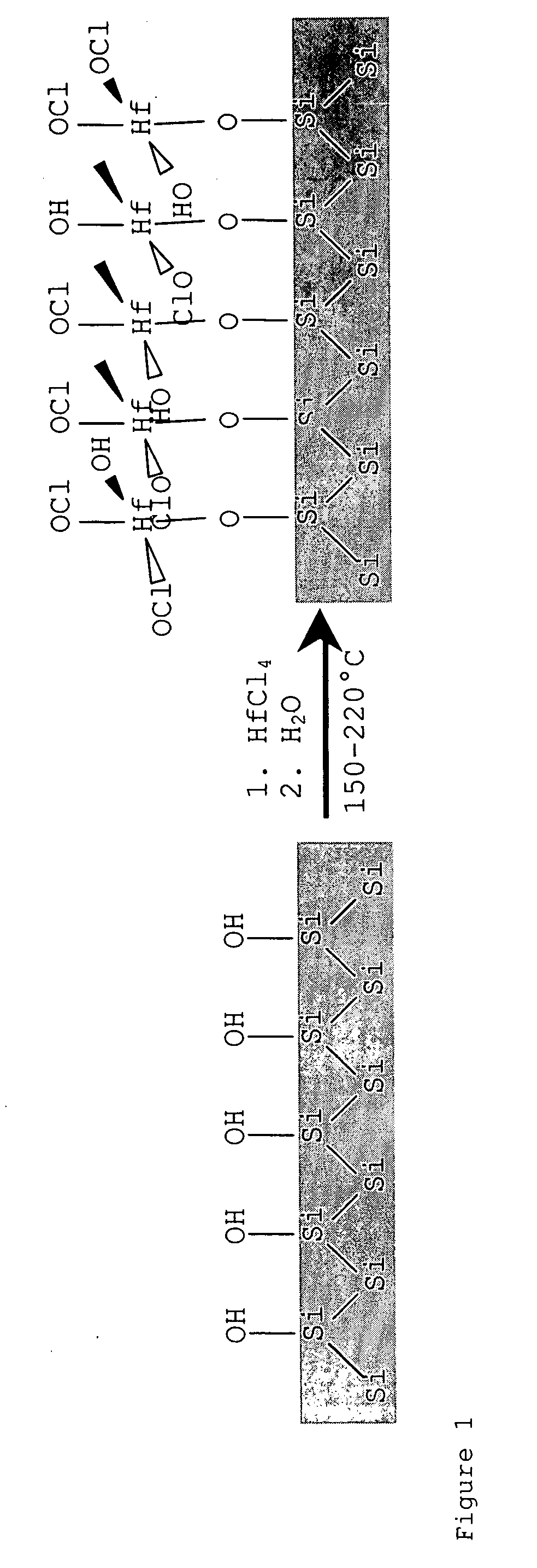
Low temperature atomic layer deposition of oxides on compound semiconductors
PatentActiveUS20160056033A1
Innovation
- A low-temperature ALD process is employed, using in-situ hydrogen and sulfur passivation to prevent Ge out-diffusion and SiOx formation, followed by an elevated temperature anneal to form high-dielectric-constant oxides like Al2O3 and HfO2, minimizing interface trap states and maintaining oxide quality.


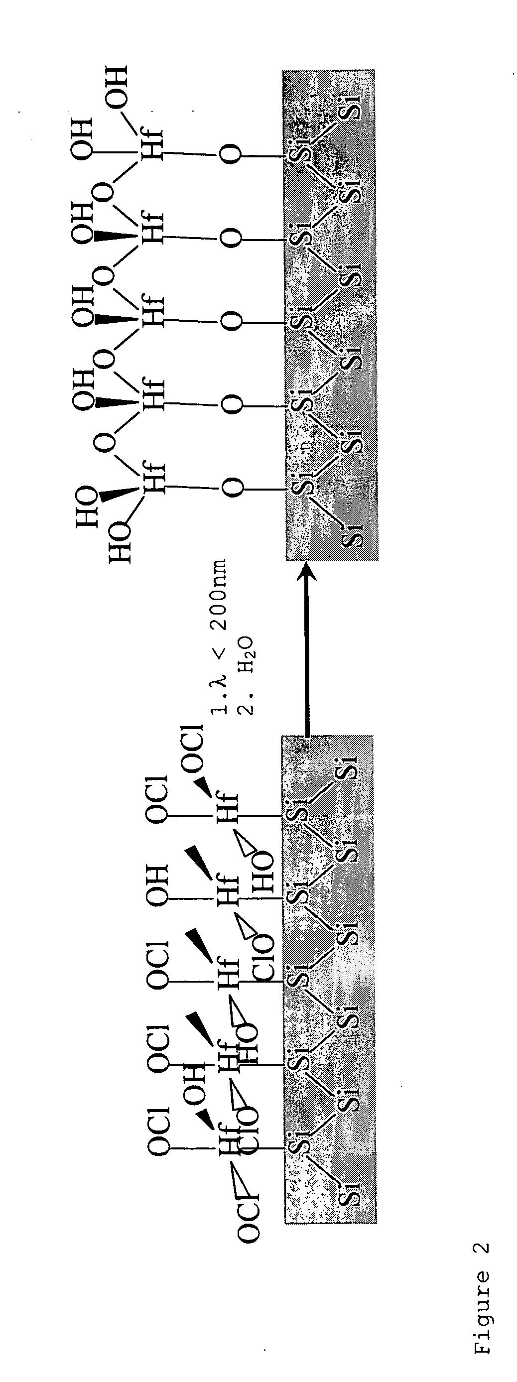
Atomic layer deposition method for depositing a layer
PatentActiveUS20070049045A1
Innovation
- An ALD method involving pulses of precursor gases, inert atmospheres, and UV irradiation to enhance hydroxyl formation and improve layer deposition, with specific wavelengths and temperatures optimizing the interface quality and reducing defects.

Environmental and Safety Regulations for ALD Processes
The environmental and safety regulatory landscape for Atomic Layer Deposition processes has become increasingly stringent as the technology scales up from research laboratories to high-volume manufacturing environments. Regulatory frameworks governing ALD operations encompass multiple jurisdictions, including the Environmental Protection Agency in the United States, the European Chemicals Agency under REACH regulations, and various national semiconductor industry standards organizations worldwide.
Chemical precursor management represents a primary regulatory focus area, as many ALD precursors contain hazardous materials such as organometallic compounds, metal halides, and reactive gases. Regulations mandate comprehensive material safety data sheet compliance, proper storage protocols, and waste disposal procedures. The semiconductor industry must adhere to strict exposure limits for workers, typically measured in parts per billion for highly toxic precursors like trimethylaluminum and titanium tetrachloride.
Emission control requirements have evolved significantly, particularly regarding volatile organic compounds and greenhouse gas emissions from ALD chambers. Regulatory bodies now require advanced abatement systems capable of achieving destruction and removal efficiencies exceeding 99% for most precursor byproducts. These systems must undergo regular performance verification and maintain detailed emission monitoring records.
Workplace safety standards specifically address the unique hazards associated with ALD processes, including requirements for emergency response procedures, personal protective equipment specifications, and facility ventilation design criteria. The Occupational Safety and Health Administration has established specific guidelines for semiconductor fabrication facilities that directly impact ALD tool installation and operation protocols.
International harmonization efforts are underway to standardize ALD safety requirements across different manufacturing regions. The International Electrotechnical Commission has developed preliminary standards addressing equipment safety, while the Semiconductor Equipment and Materials International organization continues to refine industry-specific guidelines. These evolving regulations directly influence interface defect reduction strategies by constraining allowable process parameters, precursor selection, and chamber cleaning procedures, ultimately requiring manufacturers to balance regulatory compliance with optimal deposition conditions.
Economic Impact Assessment of ALD Interface Defect Solutions
The economic implications of ALD interface defect solutions extend far beyond immediate manufacturing costs, fundamentally reshaping semiconductor industry economics. Interface defect reduction technologies represent a critical investment area where upfront research and development expenditures yield substantial long-term returns through improved device performance and reduced failure rates.
Manufacturing cost structures undergo significant transformation when implementing advanced ALD interface defect mitigation strategies. While initial capital investments for enhanced precursor delivery systems, improved chamber designs, and sophisticated monitoring equipment can increase facility setup costs by 15-25%, these investments typically achieve payback within 18-24 months through reduced scrap rates and improved yield performance.
Production efficiency gains from defect reduction create cascading economic benefits throughout the semiconductor value chain. Enhanced interface quality directly translates to improved device reliability, reducing warranty costs and field failure rates by up to 40% in critical applications. This reliability improvement enables manufacturers to command premium pricing for high-performance products while reducing long-term support obligations.
The competitive landscape shifts dramatically as companies successfully implement interface defect reduction technologies. Early adopters gain significant market advantages through superior product performance and reliability, often capturing 20-30% market share premiums in high-value segments such as automotive and aerospace semiconductors where reliability requirements are paramount.
Supply chain economics also benefit from reduced interface defects through decreased inventory requirements and improved demand predictability. Lower defect rates enable just-in-time manufacturing approaches, reducing working capital requirements by 10-15% while improving customer satisfaction through more consistent delivery schedules.
Return on investment calculations for ALD interface defect solutions typically demonstrate positive economics within two years, with ongoing benefits including reduced material waste, improved equipment utilization, and enhanced product differentiation capabilities that support sustained competitive advantages in increasingly demanding semiconductor markets.
Unlock deeper insights with PatSnap Eureka Quick Research — get a full tech report to explore trends and direct your research. Try now!
Generate Your Research Report Instantly with AI Agent
Supercharge your innovation with PatSnap Eureka AI Agent Platform!