

Ion Selective Electrode in Semiconductor Industry: Specificity
MAR 8, 20269 MIN READ
Generate Your Research Report Instantly with AI Agent
PatSnap Eureka helps you evaluate technical feasibility & market potential.
Ion Selective Electrode Semiconductor Applications and Goals
Ion selective electrodes have emerged as critical analytical instruments in semiconductor manufacturing, where precision and reliability are paramount. These electrochemical sensors provide real-time monitoring capabilities for ionic species in various process solutions, enabling manufacturers to maintain stringent quality control standards throughout fabrication processes.
The semiconductor industry's adoption of ISE technology stems from the need for continuous monitoring of ultrapure water systems, chemical mechanical planarization slurries, and etching solutions. Traditional analytical methods often require sample collection and laboratory analysis, introducing delays that can compromise production efficiency and yield optimization.
Primary applications of ion selective electrodes in semiconductor manufacturing include fluoride monitoring in hydrofluoric acid etching processes, where precise concentration control prevents substrate damage and ensures uniform etching rates. Chloride detection in cleaning solutions helps maintain equipment integrity and prevents corrosion of sensitive components. Additionally, pH monitoring through hydrogen ion selective electrodes ensures optimal chemical reaction conditions during various fabrication steps.
The technology's integration into automated process control systems represents a significant advancement in semiconductor manufacturing. Real-time data acquisition enables immediate process adjustments, reducing waste and improving overall production efficiency. This capability is particularly valuable in advanced node manufacturing, where process windows become increasingly narrow.
Current technological goals focus on enhancing electrode selectivity to minimize interference from complex chemical matrices commonly encountered in semiconductor processes. Manufacturers are pursuing improved sensor stability under extreme conditions, including high temperatures, aggressive chemicals, and radiation exposure typical in semiconductor environments.
Long-term objectives include developing miniaturized electrode arrays capable of simultaneous multi-ion detection, enabling comprehensive process monitoring through single sensor systems. Advanced signal processing algorithms and machine learning integration aim to predict process deviations before they impact product quality.
The evolution toward Industry 4.0 manufacturing paradigms drives demand for intelligent sensor networks that provide predictive maintenance capabilities and autonomous process optimization. Ion selective electrodes are positioned to play a central role in these smart manufacturing ecosystems, contributing to reduced downtime and enhanced production yields.
Future development trajectories emphasize solid-state electrode designs that eliminate traditional liquid junction limitations, offering improved reliability and reduced maintenance requirements. These innovations align with semiconductor industry demands for robust, low-maintenance analytical solutions that support continuous manufacturing operations.
Market Demand for High-Specificity ISE in Semiconductor
The semiconductor industry's relentless pursuit of miniaturization and enhanced performance has created an unprecedented demand for high-specificity ion selective electrodes. As device geometries shrink to nanometer scales and manufacturing processes become increasingly complex, the need for precise ionic contamination monitoring has evolved from a quality assurance measure to a critical manufacturing requirement. Traditional analytical methods often lack the real-time monitoring capabilities and specificity required for modern semiconductor fabrication environments.
The global semiconductor market's expansion, driven by artificial intelligence, Internet of Things, and 5G technologies, has intensified the focus on manufacturing yield optimization. Contamination-related defects represent one of the most significant yield detractors in semiconductor production, with ionic impurities being particularly problematic due to their mobility and reactivity at elevated processing temperatures. This reality has positioned high-specificity ISE technology as an essential component of advanced process control systems.
Wafer fabrication facilities increasingly require continuous monitoring of multiple ionic species simultaneously, including sodium, potassium, chloride, and fluoride ions, each demanding detection limits in the parts-per-trillion range. The market demand extends beyond traditional monitoring applications to encompass real-time process optimization, where ISE systems must provide immediate feedback for automated process adjustments. This requirement has driven specifications for response times measured in seconds rather than minutes.
The emergence of advanced packaging technologies, including through-silicon vias and wafer-level packaging, has introduced new contamination pathways that conventional monitoring approaches cannot adequately address. These applications demand ISE systems capable of operating in harsh chemical environments while maintaining exceptional selectivity ratios, often exceeding 10,000:1 for target ions versus common interferents.
Market drivers also include regulatory compliance requirements and customer quality specifications that mandate comprehensive ionic contamination documentation throughout the manufacturing process. Leading semiconductor manufacturers are increasingly specifying ISE-based monitoring systems as mandatory equipment for supplier qualification, creating a cascading demand effect throughout the supply chain.
The economic impact of contamination-related yield losses has made high-specificity ISE systems attractive investments despite their premium pricing. Facilities report that advanced ISE monitoring systems can prevent contamination events that would otherwise result in significant financial losses, making the technology's return on investment compelling for high-volume manufacturing operations.
Current ISE Specificity Challenges in Semiconductor Processes
Ion selective electrodes face significant specificity challenges in semiconductor manufacturing environments due to the complex chemical matrices and stringent purity requirements inherent to these processes. The primary challenge stems from the presence of multiple interfering ions that can compromise electrode selectivity, particularly in chemical mechanical planarization slurries, etching solutions, and cleaning chemistries where various ionic species coexist at different concentration levels.
Cross-sensitivity represents a critical limitation in current ISE implementations within semiconductor fabs. Traditional ISE sensors often exhibit unwanted responses to ions other than the target analyte, leading to measurement errors that can propagate through process control systems. For instance, fluoride-selective electrodes used in silicon etching processes may show interference from hydroxide ions or organic fluorine compounds, while pH electrodes can be affected by alkali metal ions in high-ionic-strength solutions commonly used in wafer processing.
The dynamic nature of semiconductor process chemistries poses additional specificity challenges. As process solutions age or undergo chemical reactions during manufacturing steps, the ionic composition changes continuously, creating time-dependent interference patterns that are difficult to predict and compensate for using conventional calibration methods. This temporal variability particularly affects long-term measurement stability and requires frequent recalibration cycles that disrupt production workflows.
Temperature and pressure variations in semiconductor processes further complicate ISE specificity. Many fabrication steps operate at elevated temperatures or under vacuum conditions, which can alter the selectivity coefficients of ion-selective membranes and change the relative response to target versus interfering ions. These environmental factors create additional uncertainty in measurement accuracy and limit the applicability of standard ISE technologies in critical process monitoring applications.
Matrix effects from high-purity solvents and specialized chemical additives used in semiconductor manufacturing create unique interference mechanisms not encountered in traditional analytical applications. Ultra-pure water systems, organic solvents, and proprietary chemical formulations can affect membrane permeability and electrode response characteristics in unpredictable ways, making it challenging to maintain consistent specificity across different process chemistries and manufacturing facilities.
Existing ISE Solutions for Semiconductor Ion Detection
01 Ion-selective membrane composition and ionophore selection
The specificity of ion-selective electrodes can be enhanced through careful selection of ionophores and membrane compositions. Specific ionophores are designed to selectively bind target ions while minimizing interference from other ions. The membrane matrix, typically composed of polymeric materials and plasticizers, plays a crucial role in determining the electrode's selectivity coefficient. Various ionophore structures, including crown ethers, calixarenes, and other macrocyclic compounds, can be incorporated to achieve high selectivity for specific ions such as potassium, sodium, calcium, or other cations and anions.- Ion-selective membrane composition and ionophore selection: The specificity of ion-selective electrodes can be enhanced through careful selection of ionophores and membrane compositions. Specific ionophores are designed to selectively bind target ions while minimizing interference from other ions. The membrane matrix, typically composed of polymeric materials and plasticizers, plays a crucial role in determining the electrode's selectivity coefficient. Various ionophore structures, including crown ethers, calixarenes, and other macrocyclic compounds, can be incorporated to achieve high selectivity for specific ions such as potassium, sodium, calcium, or other cations and anions.
- Interference reduction and selectivity coefficient optimization: Improving ion-selective electrode specificity involves minimizing interference from competing ions through optimization of selectivity coefficients. This can be achieved by adjusting the ratio of ionophore to membrane components, incorporating lipophilic additives, and using specific ion-excluders. The selectivity coefficient quantifies the electrode's preference for the target ion over interfering ions, and various formulation strategies can be employed to enhance this parameter. Testing methods for evaluating selectivity typically involve measuring electrode response in mixed ion solutions.
- Solid-contact and internal reference electrode design: The specificity and stability of ion-selective electrodes can be improved through advanced internal electrode designs. Solid-contact electrodes eliminate the need for internal filling solutions and provide better long-term stability. The use of conducting polymers, carbon materials, or redox-active compounds as intermediate layers between the ion-selective membrane and the electronic conductor can enhance signal transduction while maintaining selectivity. These designs reduce potential drift and improve the reproducibility of measurements.
- Multi-ion detection and sensor array systems: Ion-selective electrode specificity can be utilized in multi-ion detection systems and sensor arrays for simultaneous measurement of multiple analytes. These systems employ multiple electrodes with different selectivities, allowing for the determination of various ions in complex samples. Pattern recognition and chemometric methods can be applied to enhance discrimination between different ions and compensate for cross-sensitivities. Such approaches are particularly useful in clinical diagnostics, environmental monitoring, and process control applications.
- Electrode conditioning and surface modification techniques: The specificity of ion-selective electrodes can be maintained and enhanced through proper conditioning protocols and surface modification techniques. Pre-treatment procedures, including soaking in specific solutions and electrochemical conditioning, help establish stable boundary potentials and optimal membrane properties. Surface modifications using nanomaterials, self-assembled monolayers, or polymer coatings can improve selectivity by providing additional recognition sites or blocking interfering species. Regular maintenance and regeneration procedures ensure consistent electrode performance over extended periods.
02 Interference reduction and selectivity coefficient optimization
Improving ion-selective electrode specificity involves minimizing interference from competing ions through optimization of selectivity coefficients. This can be achieved by adjusting the ratio of ionophore to membrane components, incorporating lipophilic additives, and using specific ion-excluders. The selectivity coefficient quantifies the electrode's preference for the target ion over interfering ions, and various formulation strategies can be employed to enhance this parameter. Testing methods for evaluating selectivity typically involve measuring electrode response in mixed ion solutions.Expand Specific Solutions03 Solid-contact and internal reference electrode design
The specificity and stability of ion-selective electrodes can be improved through advanced internal electrode designs. Solid-contact electrodes eliminate the need for internal filling solutions and can provide enhanced selectivity through the use of conducting polymers or other intermediate layers. The design of the internal reference system affects the electrode's potential stability and reduces interference from sample matrix effects. Various materials including carbon-based composites and metal oxides can be used to create stable internal contacts.Expand Specific Solutions04 Multi-ion sensing and array-based detection systems
Advanced ion-selective electrode systems employ multiple electrodes with different specificities to simultaneously detect various ions or to improve overall selectivity through pattern recognition. Array-based systems can use mathematical algorithms to deconvolute signals from multiple electrodes, compensating for cross-sensitivities and enhancing specificity for target analytes. These systems may incorporate electrodes with overlapping selectivities combined with chemometric methods to achieve superior discrimination between similar ions.Expand Specific Solutions05 Surface modification and coating techniques for enhanced selectivity
The specificity of ion-selective electrodes can be enhanced through surface modification techniques including the application of selective coatings, permselective layers, or biorecognition elements. These modifications can provide additional selectivity barriers that exclude interfering species based on size, charge, or chemical properties. Techniques such as electropolymerization, self-assembled monolayers, or sol-gel coatings can be employed to create selective interfaces. Such modifications are particularly useful for improving selectivity in complex sample matrices.Expand Specific Solutions
Key Players in ISE and Semiconductor Equipment Industry
The ion selective electrode (ISE) technology in semiconductor manufacturing represents a mature yet evolving market segment within the broader analytical instrumentation industry. The competitive landscape is characterized by established players across multiple tiers, from global conglomerates to specialized manufacturers. Major Japanese corporations like Canon Inc., FUJIFILM Corp., and Hitachi High-Tech America dominate through their comprehensive semiconductor equipment portfolios and advanced materials expertise. European companies such as Robert Bosch GmbH and Endress+Hauser Conducta provide industrial automation and process control solutions. Specialized analytical companies including Radiometer A/S, HORIBA Advanced Techno, and A&T Corp. focus specifically on electrochemical sensing technologies. The market benefits from strong academic research foundations through institutions like California Institute of Technology, Zhejiang University, and Sichuan University, driving innovation in electrode materials and sensing mechanisms. Technology maturity varies across applications, with basic pH and ion measurements being well-established while advanced semiconductor-specific applications continue evolving to meet increasingly stringent purity and precision requirements in modern chip manufacturing processes.
Radiometer A/S
Technical Solution: Radiometer develops clinical-grade ion selective electrode technology adapted for semiconductor industry applications, focusing on multi-parameter analysis systems. Their ISE solutions feature simultaneous measurement of multiple ions including sodium, potassium, chloride, and pH in semiconductor processing solutions. The technology incorporates temperature compensation algorithms and automatic quality control procedures to ensure measurement accuracy across varying process conditions. Radiometer's electrodes utilize liquid membrane technology with enhanced selectivity for target ions while minimizing interference from organic compounds and surfactants commonly used in semiconductor manufacturing. Their systems include automated maintenance protocols and self-diagnostic capabilities to reduce downtime in continuous monitoring applications.
Strengths: Proven multi-parameter measurement capability with robust quality control systems and automated maintenance features. Weaknesses: Originally designed for clinical applications, may require adaptation for specific semiconductor process requirements and harsh chemical environments.
Unisense A/S
Technical Solution: Unisense develops microsensor-based ion selective electrode technology for semiconductor process monitoring with focus on spatial resolution and real-time analysis. Their ISE systems utilize glass micropipette electrodes with tip diameters in the micrometer range, enabling localized ion concentration measurements in semiconductor processing equipment. The technology incorporates advanced electrometer amplification and noise reduction techniques to achieve high sensitivity despite the small electrode size. Unisense's approach emphasizes rapid response times and minimal sample volume requirements, making their systems suitable for inline monitoring of semiconductor chemical processes where sample availability is limited and contamination must be minimized.
Strengths: Unique microsensor technology enabling high spatial resolution measurements with minimal sample requirements. Weaknesses: Fragile microsensor design may require frequent replacement and careful handling in industrial environments.
Core Innovations in ISE Membrane Selectivity Enhancement
Ion-selective electrodes
PatentInactiveUS20050191428A1
Innovation
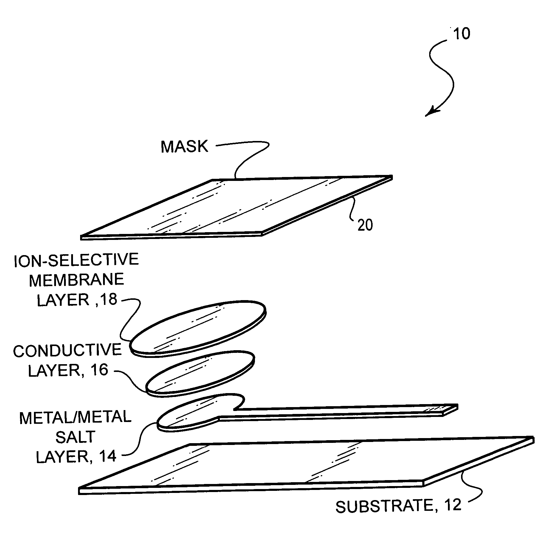
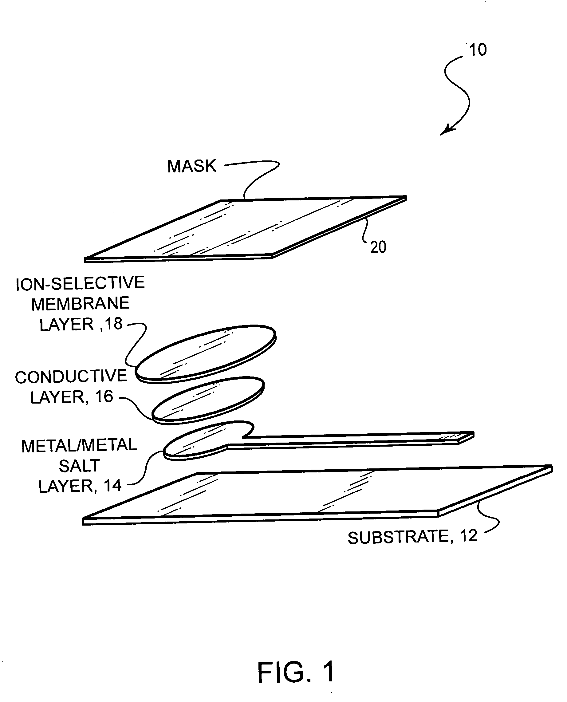
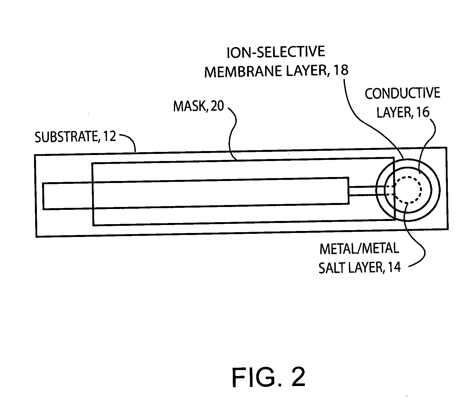
- A stable, compact ion-selective electrode design featuring a water-impermeable substrate, an electrically conductive metal/metal salt layer, a hydrophobic conductive layer with ions for stable potential, an ion-selective layer, and a water-impermeable barrier layer to prevent exposure to aqueous solutions, eliminating the need for calibration and reducing equilibration time.

Ion-selective electrodes and method of fabricating sensing units thereof
PatentInactiveUS20050263410A1
Innovation
- A metal oxide semiconductor field effect transistor (MOSFET) with a sensing unit comprising a substrate, an oxide layer, and an ammonium ion selective film is developed, where the MOSFET is connected to a conductive line, allowing for the detection of ammonium ion concentrations by analyzing voltage signals from a test solution.


Semiconductor Industry Standards for ISE Performance
The semiconductor industry has established comprehensive standards for Ion Selective Electrode (ISE) performance to ensure consistent and reliable measurements across manufacturing processes. These standards primarily focus on specificity requirements, which are critical for maintaining product quality and process control in semiconductor fabrication environments.
The International Electrotechnical Commission (IEC) and SEMI (Semiconductor Equipment and Materials International) have developed specific guidelines for ISE performance in semiconductor applications. These standards define minimum selectivity coefficients, typically requiring values below 10^-3 for primary interfering ions and below 10^-2 for secondary interferents. Such stringent requirements ensure that ISEs can accurately measure target ions even in the presence of multiple competing species commonly found in semiconductor processing solutions.
Response time specifications mandate that ISEs achieve 90% of their final reading within 30 seconds for concentration changes greater than one order of magnitude. This rapid response capability is essential for real-time process monitoring and control in high-throughput semiconductor manufacturing environments where immediate feedback is crucial for maintaining product quality.
Drift characteristics are strictly regulated, with maximum allowable drift rates of ±0.1 mV per hour under stable conditions. Long-term stability requirements specify that electrode potential should not deviate more than ±2 mV over a 24-hour period when measuring constant ionic concentrations. These stability parameters ensure consistent measurements throughout extended production runs.
Temperature compensation standards require ISEs to maintain accuracy within ±5% across the typical semiconductor processing temperature range of 15-35°C. Additionally, the standards specify minimum detection limits, typically requiring sensitivity to ion concentrations as low as 10^-6 M for critical applications such as ultrapure water monitoring and chemical bath analysis.
Calibration protocols are standardized to ensure reproducibility across different facilities and equipment. These protocols specify buffer solutions, calibration frequencies, and acceptable calibration curve parameters, including minimum slope requirements of 90% of theoretical Nernstian response for monovalent ions and appropriate adjustments for multivalent species.
Environmental Impact of ISE Manufacturing Processes
The manufacturing of ion selective electrodes for semiconductor applications presents significant environmental considerations that require careful evaluation and management. Traditional ISE production processes involve the use of various chemical compounds, including heavy metals, organic solvents, and specialized polymeric materials that can pose environmental risks if not properly handled. The fabrication of reference electrodes often requires silver chloride and potassium chloride solutions, while ion-selective membranes may incorporate plasticizers and ionophores that contain potentially hazardous substances.
Semiconductor-grade ISE manufacturing demands ultra-pure materials and cleanroom environments, leading to increased energy consumption and waste generation compared to standard analytical electrodes. The purification processes required to achieve the necessary selectivity and stability for semiconductor applications typically involve multiple chemical treatment steps, generating liquid and solid waste streams that require specialized disposal methods. Additionally, the precision manufacturing requirements result in higher rejection rates during quality control, contributing to material waste.
Water consumption represents another critical environmental factor, as ISE manufacturing requires extensive rinsing and cleaning procedures to maintain contamination-free production environments. The wastewater generated often contains trace amounts of heavy metals and organic compounds that necessitate advanced treatment before discharge. Furthermore, the packaging and preservation of semiconductor-grade ISEs typically require inert atmospheres and specialized storage materials, adding to the overall environmental footprint.
Recent developments in green manufacturing approaches have begun addressing these environmental concerns through the implementation of closed-loop systems, solvent recovery processes, and the development of more environmentally benign electrode materials. Some manufacturers are exploring bio-compatible ionophores and recyclable membrane materials to reduce the long-term environmental impact. The adoption of lean manufacturing principles and waste minimization strategies has also shown promise in reducing the overall environmental burden of ISE production for semiconductor applications.
The regulatory landscape surrounding ISE manufacturing continues to evolve, with stricter environmental compliance requirements driving innovation in cleaner production technologies and sustainable material selection for semiconductor industry applications.
Unlock deeper insights with PatSnap Eureka Quick Research — get a full tech report to explore trends and direct your research. Try now!
Generate Your Research Report Instantly with AI Agent
Supercharge your innovation with PatSnap Eureka AI Agent Platform!