

Maximize VLSI Process Efficiency for 5G Network Components
MAR 7, 20269 MIN READ
Generate Your Research Report Instantly with AI Agent
Patsnap Eureka helps you evaluate technical feasibility & market potential.
VLSI Process Background and 5G Component Goals
Very Large Scale Integration (VLSI) technology has undergone remarkable evolution since its inception in the 1970s, transitioning from simple integrated circuits to complex systems-on-chip capable of handling billions of transistors. The progression from micrometer to nanometer fabrication processes has enabled unprecedented miniaturization and performance improvements, establishing VLSI as the cornerstone of modern semiconductor manufacturing.
The advent of 5G wireless communication technology has introduced stringent requirements for semiconductor components, demanding higher frequencies, lower latency, and enhanced power efficiency. Traditional VLSI processes, optimized for previous generation technologies, face significant challenges in meeting these demanding specifications while maintaining cost-effectiveness and manufacturing yield.
Contemporary 5G network infrastructure relies heavily on specialized semiconductor components including radio frequency integrated circuits, baseband processors, millimeter-wave transceivers, and massive MIMO antenna arrays. These components operate at frequencies ranging from sub-6 GHz to millimeter-wave bands exceeding 28 GHz, requiring advanced process technologies with feature sizes below 7 nanometers to achieve necessary performance metrics.
The primary technical objectives for VLSI process optimization in 5G applications encompass several critical areas. Enhanced transistor switching speeds are essential to support the high-frequency operations required for 5G signal processing, while improved power efficiency directly impacts battery life in mobile devices and operational costs in base station infrastructure.
Thermal management represents another crucial goal, as 5G components generate substantial heat during high-frequency operations. Advanced VLSI processes must incorporate innovative heat dissipation techniques and thermal-aware design methodologies to ensure reliable operation under demanding conditions.
Manufacturing yield optimization remains paramount, particularly given the complexity of 5G-specific integrated circuits. Process variations that were acceptable in previous technology generations can significantly impact 5G component performance, necessitating tighter process control and advanced statistical process monitoring techniques.
Integration density improvements enable the incorporation of multiple 5G functions within single chip solutions, reducing system complexity and improving overall network efficiency. This consolidation approach requires sophisticated process technologies capable of supporting diverse circuit types, from high-frequency analog components to complex digital signal processors, within unified manufacturing flows.
Market Demand for 5G VLSI Components
The global telecommunications industry is experiencing unprecedented transformation driven by 5G network deployment, creating substantial demand for specialized VLSI components optimized for next-generation wireless infrastructure. Network equipment manufacturers require increasingly sophisticated semiconductor solutions to support enhanced mobile broadband, ultra-reliable low-latency communications, and massive machine-type communications applications.
Base station infrastructure represents the largest market segment for 5G VLSI components, encompassing radio frequency integrated circuits, digital signal processors, and power management units. Telecommunications operators worldwide are investing heavily in network densification strategies, requiring millions of small cells and macro base stations equipped with advanced semiconductor solutions. The transition from 4G to 5G necessitates complete hardware upgrades across existing network infrastructure.
Mobile device manufacturers constitute another critical demand driver, requiring application processors, modem chipsets, and antenna tuning components capable of supporting multiple 5G frequency bands simultaneously. The proliferation of 5G-enabled smartphones, tablets, and Internet of Things devices creates sustained volume demand for cost-effective yet high-performance VLSI solutions.
Industrial and automotive sectors are emerging as significant growth markets for 5G VLSI components. Manufacturing facilities implementing Industry 4.0 initiatives require wireless communication modules supporting real-time control systems and predictive maintenance applications. Autonomous vehicle development programs demand ultra-low latency communication processors for vehicle-to-everything connectivity.
Edge computing infrastructure deployment amplifies demand for specialized processors and memory controllers optimized for distributed 5G network architectures. Cloud service providers and telecommunications operators are establishing thousands of edge data centers requiring purpose-built semiconductor solutions for network function virtualization and software-defined networking applications.
Supply chain constraints and geopolitical considerations are reshaping procurement patterns, with network operators seeking diversified supplier bases and domestically manufactured components. This trend creates opportunities for regional VLSI manufacturers to capture market share through localized production capabilities and customized solutions tailored to specific geographic requirements.
The market exhibits strong growth momentum driven by government initiatives promoting 5G adoption, increasing data consumption patterns, and emerging applications requiring high-bandwidth, low-latency connectivity. Private network deployments across enterprise segments further expand addressable market opportunities for specialized VLSI component suppliers.
Current VLSI Process Challenges for 5G Applications
The VLSI manufacturing process for 5G network components faces unprecedented complexity challenges as device geometries continue to shrink below 7nm nodes. Traditional lithography techniques struggle with the precision requirements needed for advanced FinFET and Gate-All-Around (GAA) transistor structures essential for 5G RF front-end modules and baseband processors. The increasing variability in critical dimensions becomes particularly problematic when manufacturing millimeter-wave components that operate at frequencies exceeding 24 GHz, where even minor dimensional variations can significantly impact performance.
Thermal management presents another critical bottleneck in current VLSI processes for 5G applications. The high power density requirements of 5G chipsets, combined with the reduced thermal conductivity pathways in advanced node architectures, create substantial heat dissipation challenges during fabrication. This thermal stress affects dopant activation profiles and can cause unwanted diffusion in ultra-shallow junctions, directly impacting the high-frequency performance characteristics crucial for 5G signal processing.
Process integration complexity has escalated dramatically with the introduction of heterogeneous integration requirements for 5G systems. Current fabrication flows struggle to accommodate the simultaneous processing of different material systems, including III-V compounds for RF components, silicon photonics for optical interconnects, and advanced CMOS logic on the same substrate. The incompatibility between processing temperatures and chemical environments for these diverse materials creates yield and reliability concerns.
Defect density control remains a persistent challenge, particularly for 5G-specific structures such as massive MIMO antenna arrays and beamforming circuits. The increased transistor count and interconnect complexity in these applications amplify the impact of random defects, while systematic process variations can cause performance mismatches across array elements. Current inspection and metrology capabilities often lack the resolution and throughput needed to detect critical defects in these dense, high-frequency circuits.
Manufacturing cost escalation represents a fundamental economic challenge, with mask costs alone exceeding $10 million for leading-edge nodes. The specialized equipment requirements for 5G component fabrication, including advanced EUV lithography systems and precision ion implantation tools, significantly increase capital expenditure requirements while reducing manufacturing flexibility and increasing process cycle times.
Current VLSI Process Optimization Solutions
01 Advanced lithography and patterning techniques
Improving VLSI process efficiency through enhanced lithography methods that enable finer feature resolution and better pattern transfer. These techniques focus on optimizing exposure systems, mask technologies, and resolution enhancement methods to achieve smaller geometries with higher precision. Advanced patterning approaches help reduce defects and improve yield in semiconductor manufacturing processes.- Advanced lithography and patterning techniques: Improving VLSI process efficiency through enhanced lithography methods that enable finer feature resolution and more precise pattern transfer. These techniques include advanced photolithography processes, multi-patterning strategies, and optimized exposure methods that reduce defects and improve yield. The implementation of these methods allows for better control over critical dimensions and reduces the number of processing steps required, thereby increasing overall manufacturing efficiency.
- Process integration and workflow optimization: Enhancing efficiency through streamlined process integration that combines multiple manufacturing steps and reduces cycle time. This includes optimizing the sequence of deposition, etching, and cleaning processes, as well as implementing in-situ processing techniques that eliminate intermediate steps. The approach focuses on reducing wafer handling, minimizing contamination risks, and improving throughput by consolidating compatible process steps into unified modules.
- Defect detection and yield enhancement: Implementing advanced inspection and metrology systems to identify and reduce defects throughout the manufacturing process. These systems utilize sophisticated algorithms and sensing technologies to detect anomalies at various stages of production, enabling real-time process adjustments. The methodology includes automated defect classification, root cause analysis, and feedback mechanisms that continuously improve process parameters to maximize yield and reduce waste.
- Equipment utilization and automation: Maximizing process efficiency through intelligent equipment scheduling, automated material handling, and predictive maintenance systems. This involves implementing smart factory concepts where equipment downtime is minimized through predictive analytics, and production flow is optimized using real-time data. The systems incorporate machine learning algorithms to predict equipment failures, optimize maintenance schedules, and automatically adjust processing parameters to maintain consistent output quality while reducing operational costs.
- Chemical mechanical planarization and surface preparation: Improving process efficiency through optimized planarization techniques that ensure uniform surface topology for subsequent processing steps. These methods focus on achieving consistent material removal rates, reducing surface defects, and minimizing the number of polishing steps required. The techniques include advanced slurry formulations, optimized pad designs, and process control strategies that enhance throughput while maintaining stringent surface quality requirements for multi-layer device fabrication.
02 Process automation and control systems
Implementation of automated control systems and real-time monitoring to enhance manufacturing efficiency in VLSI fabrication. These systems utilize advanced algorithms and feedback mechanisms to optimize process parameters, reduce cycle times, and minimize human intervention. Automation technologies help maintain consistent quality while increasing throughput and reducing operational costs.Expand Specific Solutions03 Defect detection and yield optimization
Methods for identifying and reducing defects during VLSI manufacturing to improve overall process yield. These approaches include inspection techniques, defect classification systems, and corrective action protocols that help minimize waste and enhance production efficiency. Advanced detection systems enable early identification of process variations and quality issues.Expand Specific Solutions04 Multi-layer processing and integration
Techniques for efficient processing of multiple layers in VLSI devices, including deposition, etching, and planarization methods. These processes focus on optimizing layer-to-layer alignment, reducing processing steps, and improving material utilization. Integration strategies help streamline manufacturing workflows and reduce overall production time while maintaining device performance.Expand Specific Solutions05 Thermal management and energy efficiency
Solutions for managing thermal processes and reducing energy consumption in VLSI fabrication. These include optimized annealing techniques, efficient heating and cooling systems, and power management strategies that reduce operational costs. Thermal control methods help improve process stability and device reliability while minimizing environmental impact.Expand Specific Solutions
Key Players in 5G VLSI Manufacturing Industry
The VLSI process efficiency optimization for 5G network components represents a rapidly evolving competitive landscape characterized by intense technological advancement and substantial market opportunities. The industry is currently in a mature growth phase, with the global 5G infrastructure market projected to reach hundreds of billions by 2030, driven by widespread network deployment and component miniaturization demands. Technology maturity varies significantly across players, with established semiconductor leaders like Samsung Electronics, Qualcomm, and Huawei Technologies demonstrating advanced VLSI capabilities through their integrated device manufacturing and design expertise. Traditional telecommunications equipment providers including Ericsson, Nokia Technologies, and LG Electronics are leveraging their network infrastructure knowledge to optimize component efficiency. Emerging specialized players like Parallel Wireless and regional telecommunications companies such as China Mobile and KT Corp are contributing domain-specific innovations. The competitive dynamics reflect a convergence of semiconductor manufacturing prowess, 5G system integration capabilities, and process optimization expertise, creating opportunities for both established giants and specialized innovators.
Samsung Electronics Co., Ltd.
Technical Solution: Samsung combines its foundry capabilities with 5G component design expertise, utilizing their 3nm GAA (Gate-All-Around) process technology for next-generation 5G chipsets. Their VLSI optimization approach focuses on FinFET scaling and advanced packaging solutions like 2.5D/3D integration for 5G base station processors. Samsung employs AI-driven design automation tools for parasitic extraction and timing closure, achieving 15% better power-performance-area (PPA) metrics compared to previous generation processes. Their comprehensive design-for-manufacturing (DFM) methodology ensures high yield rates for complex 5G SoCs, with particular emphasis on thermal management and signal integrity optimization for mmWave applications.
Strengths: Vertical integration from foundry to final products, cutting-edge process technology leadership. Weaknesses: Limited market share in 5G infrastructure compared to baseband expertise.
Huawei Technologies Co., Ltd.
Technical Solution: Huawei's VLSI process efficiency strategy centers on their Kirin 5G chipsets and Kunpeng processors, emphasizing heterogeneous computing architectures optimized for 5G network functions. Their design methodology incorporates advanced clock gating techniques and power island partitioning to minimize dynamic and static power consumption. Huawei utilizes proprietary EDA tools for floorplanning optimization and employs statistical static timing analysis (SSTA) to handle process variations in 7nm and below technologies. Their 5G base station chips feature specialized VLSI architectures with dedicated accelerators for beamforming and massive MIMO processing, achieving 40% better energy efficiency compared to conventional implementations through custom instruction set architectures and optimized memory hierarchies.
Strengths: Strong system-level integration capabilities and comprehensive 5G ecosystem. Weaknesses: Limited access to advanced EDA tools and foundry services due to trade restrictions.
Core VLSI Process Innovations for 5G Efficiency
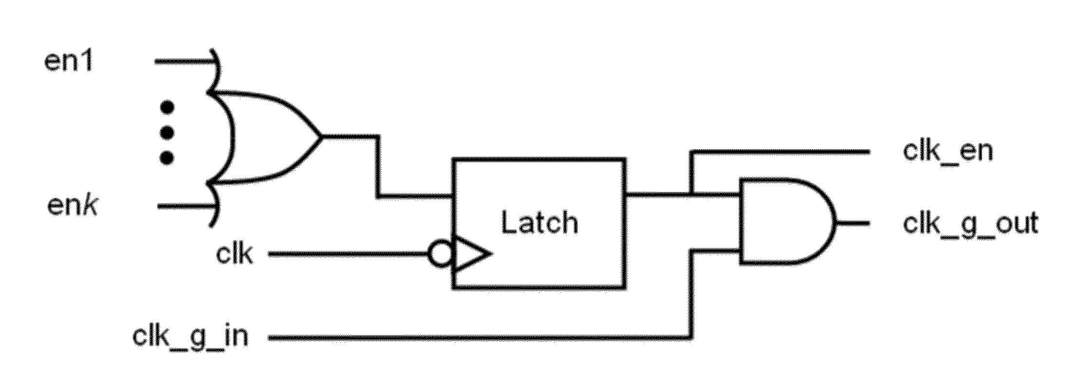
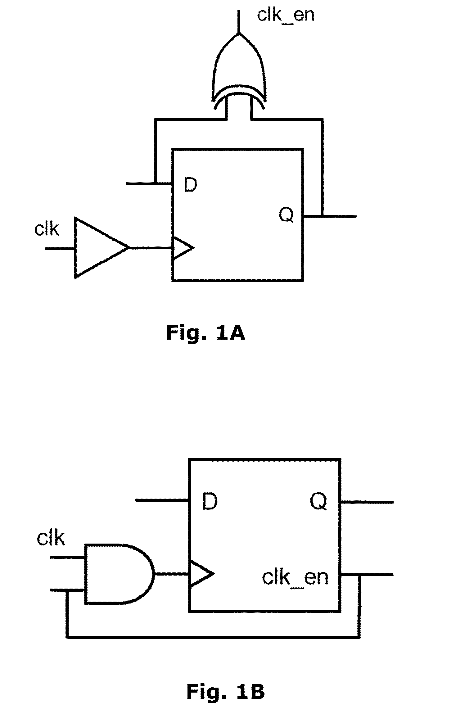
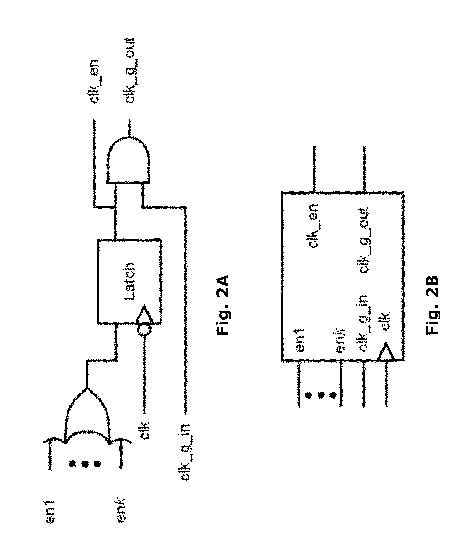
Method for optimizing power in a very large scale integration (VLSI) design by detecting clock gating opportunities
PatentInactiveUS7509606B2
Innovation
- A computer-implemented method for generating statistics on clock-gated components within a chip to identify opportunities for power savings through clock gating testing, which involves identifying non-clock gated components and generating statistics to determine if they can be clock gated, thereby reducing power consumption.


System and method for generating a clock gating network for logic circuits
PatentInactiveUS20130194016A1
Innovation
- A probabilistic model for clock gating networks is developed, which determines toggling probabilities of flip-flops, clusters correlated flip-flops, and provides a common gater for each cluster, enabling significant power savings by disabling the clock signal only when necessary, thereby reducing switching power consumption.

Supply Chain Risk Management for VLSI Manufacturing
The VLSI manufacturing ecosystem for 5G network components faces unprecedented supply chain vulnerabilities that directly impact process efficiency optimization efforts. Global semiconductor shortages have exposed critical dependencies on specialized materials, equipment, and manufacturing capabilities concentrated in specific geographic regions. These vulnerabilities create cascading effects that can disrupt carefully orchestrated efficiency improvement initiatives.
Raw material procurement represents the most fundamental risk layer in VLSI manufacturing. Ultra-pure silicon wafers, rare earth elements for dopants, and specialized chemicals required for etching and cleaning processes often originate from limited supplier bases. Geopolitical tensions and trade restrictions have created additional complexity, forcing manufacturers to diversify sourcing strategies while maintaining stringent quality standards essential for 5G component performance.
Equipment supply chain risks pose equally significant challenges to process efficiency maximization. Advanced lithography systems, ion implantation tools, and metrology equipment are produced by a handful of specialized vendors with extended lead times. Any disruption in equipment availability or maintenance support can halt production lines optimized for continuous operation, undermining efficiency gains achieved through process improvements.
Manufacturing capacity constraints across the global foundry network create bottlenecks that limit efficiency optimization potential. The concentration of advanced node capabilities in specific regions increases vulnerability to natural disasters, pandemic-related shutdowns, and infrastructure failures. These risks are amplified for 5G components requiring cutting-edge process technologies with limited alternative manufacturing sources.
Intellectual property and technology transfer risks add another dimension to supply chain management. Collaborative relationships with equipment vendors, material suppliers, and foundry partners involve sharing sensitive process parameters and proprietary techniques. Protecting these assets while maintaining necessary partnerships requires sophisticated risk assessment frameworks and contractual safeguards.
Mitigation strategies must balance risk reduction with efficiency objectives. Dual sourcing arrangements, strategic inventory management, and supplier qualification programs help reduce dependency risks but may increase operational complexity. Advanced analytics and real-time monitoring systems enable proactive risk identification and response, supporting both supply chain resilience and process efficiency goals in VLSI manufacturing for 5G applications.
Yield Enhancement Strategies for 5G Component Production
Yield enhancement in 5G component production represents a critical factor in achieving cost-effective manufacturing while meeting the stringent performance requirements of next-generation wireless infrastructure. The complexity of 5G components, particularly those operating at millimeter-wave frequencies, demands sophisticated yield optimization approaches that address both traditional semiconductor challenges and emerging 5G-specific requirements.
Statistical process control implementation forms the foundation of effective yield enhancement strategies. Advanced monitoring systems utilizing real-time data analytics enable manufacturers to identify process variations before they impact production outcomes. Machine learning algorithms analyze historical production data to predict potential yield issues, allowing for proactive adjustments to manufacturing parameters. These predictive models consider multiple variables including temperature fluctuations, chemical concentrations, and equipment performance metrics.
Design for manufacturability principles play an increasingly important role in 5G component yield optimization. Engineers must balance aggressive performance targets with manufacturing constraints, particularly for components operating above 24 GHz frequencies. Layout optimization techniques, including careful consideration of critical dimension uniformity and overlay accuracy, directly impact final yield rates. Advanced design rule checking tools specifically calibrated for 5G applications help identify potential manufacturing bottlenecks during the design phase.
Defect density reduction strategies focus on contamination control and process stability enhancement. Cleanroom protocols require heightened attention to particle control, as even minor contaminations can significantly impact high-frequency component performance. Advanced metrology systems provide inline monitoring capabilities, enabling immediate detection and correction of process deviations that could compromise yield.
Adaptive process control systems represent an emerging approach to yield enhancement, utilizing artificial intelligence to continuously optimize manufacturing parameters based on real-time feedback. These systems can automatically adjust lithography exposure conditions, etch parameters, and deposition rates to maintain optimal process windows. The integration of advanced process control with predictive maintenance schedules further enhances overall equipment effectiveness and reduces unexpected downtime that impacts yield performance.
Unlock deeper insights with Patsnap Eureka Quick Research — get a full tech report to explore trends and direct your research. Try now!
Generate Your Research Report Instantly with AI Agent
Supercharge your innovation with Patsnap Eureka AI Agent Platform!