

Neuromorphic Photonic Computing for Ultra-Fast Natural Language Processing
JUN 2, 202610 MIN READ
Generate Your Research Report Instantly with AI Agent
PatSnap Eureka helps you evaluate technical feasibility & market potential.
Neuromorphic Photonic Computing Background and NLP Goals
Neuromorphic photonic computing represents a revolutionary convergence of brain-inspired computing architectures and photonic technologies, emerging from decades of research in both neuroscience and optical engineering. This paradigm draws inspiration from the human brain's neural networks, where information processing occurs through interconnected neurons communicating via electrical and chemical signals. The photonic implementation leverages light-based components to mimic these neural processes, offering unprecedented advantages in speed, energy efficiency, and parallel processing capabilities.
The foundational concept of neuromorphic computing originated in the 1980s with Carver Mead's pioneering work on analog VLSI systems that emulated neural structures. However, the integration with photonic technologies began gaining momentum in the 2000s as researchers recognized the inherent advantages of optical systems for neural network implementations. Photonic neural networks exploit the properties of light, including wavelength division multiplexing, high bandwidth, and minimal crosstalk, to create massively parallel computing architectures that can process information at the speed of light.
The evolution toward neuromorphic photonic systems has been driven by the limitations of traditional electronic processors in handling the computational demands of artificial intelligence applications. While electronic neuromorphic chips have demonstrated significant progress, they still face constraints related to power consumption, heat generation, and interconnect bottlenecks. Photonic implementations address these challenges by utilizing optical interconnects, which can carry multiple data streams simultaneously through wavelength multiplexing, and by operating with significantly lower power requirements for data transmission.
In the context of natural language processing, the computational requirements have grown exponentially with the development of large language models and transformer architectures. Modern NLP applications demand ultra-fast processing of sequential data, complex attention mechanisms, and massive matrix operations that strain conventional computing systems. The primary goal of applying neuromorphic photonic computing to NLP is to achieve breakthrough performance in processing speed while maintaining energy efficiency and scalability.
The specific objectives for neuromorphic photonic computing in NLP applications encompass several critical performance targets. First, achieving sub-microsecond response times for real-time language understanding and generation tasks, which is essential for interactive AI systems and edge computing applications. Second, enabling parallel processing of multiple language streams simultaneously, supporting multilingual and multi-modal processing scenarios that are increasingly important in global applications.
Another crucial goal involves implementing efficient attention mechanisms that are fundamental to transformer-based language models. Neuromorphic photonic systems aim to realize these attention computations through optical matrix-vector multiplications and nonlinear activation functions, potentially reducing the computational complexity from quadratic to linear scaling with sequence length. This advancement could enable processing of much longer text sequences than currently feasible with electronic systems.
The ultimate vision encompasses developing neuromorphic photonic processors capable of handling complete end-to-end NLP pipelines, from tokenization and embedding generation to complex reasoning and text generation, all within integrated photonic circuits. This would represent a paradigm shift toward optical AI accelerators specifically optimized for language processing tasks, potentially enabling new applications in real-time translation, conversational AI, and intelligent content analysis that require both high performance and energy efficiency.
The foundational concept of neuromorphic computing originated in the 1980s with Carver Mead's pioneering work on analog VLSI systems that emulated neural structures. However, the integration with photonic technologies began gaining momentum in the 2000s as researchers recognized the inherent advantages of optical systems for neural network implementations. Photonic neural networks exploit the properties of light, including wavelength division multiplexing, high bandwidth, and minimal crosstalk, to create massively parallel computing architectures that can process information at the speed of light.
The evolution toward neuromorphic photonic systems has been driven by the limitations of traditional electronic processors in handling the computational demands of artificial intelligence applications. While electronic neuromorphic chips have demonstrated significant progress, they still face constraints related to power consumption, heat generation, and interconnect bottlenecks. Photonic implementations address these challenges by utilizing optical interconnects, which can carry multiple data streams simultaneously through wavelength multiplexing, and by operating with significantly lower power requirements for data transmission.
In the context of natural language processing, the computational requirements have grown exponentially with the development of large language models and transformer architectures. Modern NLP applications demand ultra-fast processing of sequential data, complex attention mechanisms, and massive matrix operations that strain conventional computing systems. The primary goal of applying neuromorphic photonic computing to NLP is to achieve breakthrough performance in processing speed while maintaining energy efficiency and scalability.
The specific objectives for neuromorphic photonic computing in NLP applications encompass several critical performance targets. First, achieving sub-microsecond response times for real-time language understanding and generation tasks, which is essential for interactive AI systems and edge computing applications. Second, enabling parallel processing of multiple language streams simultaneously, supporting multilingual and multi-modal processing scenarios that are increasingly important in global applications.
Another crucial goal involves implementing efficient attention mechanisms that are fundamental to transformer-based language models. Neuromorphic photonic systems aim to realize these attention computations through optical matrix-vector multiplications and nonlinear activation functions, potentially reducing the computational complexity from quadratic to linear scaling with sequence length. This advancement could enable processing of much longer text sequences than currently feasible with electronic systems.
The ultimate vision encompasses developing neuromorphic photonic processors capable of handling complete end-to-end NLP pipelines, from tokenization and embedding generation to complex reasoning and text generation, all within integrated photonic circuits. This would represent a paradigm shift toward optical AI accelerators specifically optimized for language processing tasks, potentially enabling new applications in real-time translation, conversational AI, and intelligent content analysis that require both high performance and energy efficiency.
Market Demand for Ultra-Fast NLP Processing Solutions
The global demand for ultra-fast natural language processing solutions has experienced unprecedented growth, driven by the exponential increase in unstructured data generation and the need for real-time language understanding across multiple industries. Traditional computing architectures face significant bottlenecks when processing complex NLP tasks at scale, creating substantial market opportunities for revolutionary approaches like neuromorphic photonic computing.
Enterprise applications represent the largest demand segment, where organizations require instantaneous language translation, sentiment analysis, and document processing capabilities. Financial institutions need microsecond-level processing for algorithmic trading based on news sentiment, while healthcare systems demand rapid analysis of medical literature and patient records. The telecommunications sector requires real-time language processing for network optimization and customer service automation.
The artificial intelligence and machine learning market segment demonstrates particularly strong demand for ultra-fast NLP processing. Current GPU-based solutions struggle with the computational intensity of large language models, especially when handling multiple concurrent requests. Cloud service providers face increasing pressure to deliver faster response times while managing energy consumption, creating demand for more efficient processing architectures.
Autonomous systems and robotics applications present emerging demand drivers, where real-time language understanding is critical for human-machine interaction. Smart city infrastructure, autonomous vehicles, and industrial automation systems require instantaneous processing of voice commands and textual information to ensure safety and operational efficiency.
The cybersecurity sector shows growing demand for ultra-fast NLP processing to analyze threat intelligence, detect anomalies in communication patterns, and process security logs in real-time. Traditional security systems cannot keep pace with the volume and velocity of modern cyber threats, necessitating breakthrough processing capabilities.
Market demand is further amplified by the proliferation of edge computing applications, where local processing requirements eliminate the latency associated with cloud-based solutions. Internet of Things devices, mobile applications, and embedded systems increasingly require on-device NLP capabilities that current silicon-based processors cannot efficiently deliver within power and thermal constraints.
The convergence of these demand drivers creates a substantial market opportunity for neuromorphic photonic computing solutions that can deliver the required processing speed, energy efficiency, and scalability that traditional architectures cannot achieve.
Enterprise applications represent the largest demand segment, where organizations require instantaneous language translation, sentiment analysis, and document processing capabilities. Financial institutions need microsecond-level processing for algorithmic trading based on news sentiment, while healthcare systems demand rapid analysis of medical literature and patient records. The telecommunications sector requires real-time language processing for network optimization and customer service automation.
The artificial intelligence and machine learning market segment demonstrates particularly strong demand for ultra-fast NLP processing. Current GPU-based solutions struggle with the computational intensity of large language models, especially when handling multiple concurrent requests. Cloud service providers face increasing pressure to deliver faster response times while managing energy consumption, creating demand for more efficient processing architectures.
Autonomous systems and robotics applications present emerging demand drivers, where real-time language understanding is critical for human-machine interaction. Smart city infrastructure, autonomous vehicles, and industrial automation systems require instantaneous processing of voice commands and textual information to ensure safety and operational efficiency.
The cybersecurity sector shows growing demand for ultra-fast NLP processing to analyze threat intelligence, detect anomalies in communication patterns, and process security logs in real-time. Traditional security systems cannot keep pace with the volume and velocity of modern cyber threats, necessitating breakthrough processing capabilities.
Market demand is further amplified by the proliferation of edge computing applications, where local processing requirements eliminate the latency associated with cloud-based solutions. Internet of Things devices, mobile applications, and embedded systems increasingly require on-device NLP capabilities that current silicon-based processors cannot efficiently deliver within power and thermal constraints.
The convergence of these demand drivers creates a substantial market opportunity for neuromorphic photonic computing solutions that can deliver the required processing speed, energy efficiency, and scalability that traditional architectures cannot achieve.
Current State and Challenges of Neuromorphic Photonic Systems
Neuromorphic photonic systems represent a convergence of brain-inspired computing architectures with photonic technologies, aiming to replicate neural network functionalities using light-based components. Current implementations primarily utilize silicon photonic platforms integrated with electronic control systems, where optical signals serve as information carriers while maintaining the parallel processing capabilities inherent in biological neural networks. These systems leverage wavelength division multiplexing, optical interference, and nonlinear optical effects to perform matrix operations and activation functions essential for neural network computations.
The technological maturity of neuromorphic photonic systems remains in early developmental stages, with most demonstrations confined to laboratory environments and proof-of-concept implementations. Existing prototypes typically operate at limited scales, supporting neural networks with hundreds to thousands of neurons, significantly smaller than the millions of parameters required for practical natural language processing applications. Current systems achieve processing speeds in the gigahertz range, demonstrating potential for ultra-fast computation, yet face substantial limitations in terms of programmability and reconfigurability compared to their electronic counterparts.
Integration challenges represent a primary bottleneck in current neuromorphic photonic implementations. The seamless interface between optical processing units and electronic control systems requires sophisticated analog-to-digital conversion mechanisms, introducing latency and power consumption overhead that partially negates the inherent advantages of photonic computation. Additionally, the precision and stability of optical components, particularly in maintaining consistent phase relationships and amplitude control across large-scale arrays, present significant engineering challenges that limit system reliability and accuracy.
Scalability constraints pose another fundamental challenge for neuromorphic photonic systems targeting natural language processing applications. Current fabrication technologies struggle to produce the dense, uniform optical component arrays necessary for implementing large-scale neural networks. Manufacturing variations in photonic devices lead to parameter mismatches that accumulate across network layers, degrading overall system performance and requiring complex calibration procedures that complicate practical deployment.
Power efficiency, while theoretically advantageous in photonic systems, faces practical limitations due to the energy requirements of laser sources, optical modulators, and photodetectors. Current implementations often require continuous optical pumping and active thermal management to maintain operational stability, resulting in power consumption levels that may not significantly outperform optimized electronic neural network accelerators for equivalent computational tasks.
The programming and training methodologies for neuromorphic photonic systems remain underdeveloped compared to established electronic neural network frameworks. Existing approaches require hybrid training procedures where network parameters are optimized in simulation before physical implementation, limiting the adaptability and learning capabilities that characterize advanced natural language processing systems. This constraint particularly impacts applications requiring real-time learning and adaptation to evolving language patterns and contexts.
The technological maturity of neuromorphic photonic systems remains in early developmental stages, with most demonstrations confined to laboratory environments and proof-of-concept implementations. Existing prototypes typically operate at limited scales, supporting neural networks with hundreds to thousands of neurons, significantly smaller than the millions of parameters required for practical natural language processing applications. Current systems achieve processing speeds in the gigahertz range, demonstrating potential for ultra-fast computation, yet face substantial limitations in terms of programmability and reconfigurability compared to their electronic counterparts.
Integration challenges represent a primary bottleneck in current neuromorphic photonic implementations. The seamless interface between optical processing units and electronic control systems requires sophisticated analog-to-digital conversion mechanisms, introducing latency and power consumption overhead that partially negates the inherent advantages of photonic computation. Additionally, the precision and stability of optical components, particularly in maintaining consistent phase relationships and amplitude control across large-scale arrays, present significant engineering challenges that limit system reliability and accuracy.
Scalability constraints pose another fundamental challenge for neuromorphic photonic systems targeting natural language processing applications. Current fabrication technologies struggle to produce the dense, uniform optical component arrays necessary for implementing large-scale neural networks. Manufacturing variations in photonic devices lead to parameter mismatches that accumulate across network layers, degrading overall system performance and requiring complex calibration procedures that complicate practical deployment.
Power efficiency, while theoretically advantageous in photonic systems, faces practical limitations due to the energy requirements of laser sources, optical modulators, and photodetectors. Current implementations often require continuous optical pumping and active thermal management to maintain operational stability, resulting in power consumption levels that may not significantly outperform optimized electronic neural network accelerators for equivalent computational tasks.
The programming and training methodologies for neuromorphic photonic systems remain underdeveloped compared to established electronic neural network frameworks. Existing approaches require hybrid training procedures where network parameters are optimized in simulation before physical implementation, limiting the adaptability and learning capabilities that characterize advanced natural language processing systems. This constraint particularly impacts applications requiring real-time learning and adaptation to evolving language patterns and contexts.
Existing Photonic NLP Processing Solutions
01 Photonic neural network architectures for high-speed processing
Advanced photonic neural network designs that leverage optical components to achieve ultra-fast processing speeds in neuromorphic computing systems. These architectures utilize light-based signal processing to overcome the speed limitations of traditional electronic neural networks, enabling parallel computation and reduced latency in artificial intelligence applications.- Photonic neural network architectures for high-speed processing: Advanced photonic neural network designs that leverage optical components to achieve ultra-fast computation speeds in neuromorphic systems. These architectures utilize light-based signal processing to overcome the speed limitations of traditional electronic neural networks, enabling parallel processing of multiple data streams simultaneously through optical pathways.
- Optical interconnect systems for accelerated data transmission: Implementation of optical interconnection technologies that significantly reduce latency and increase bandwidth in neuromorphic computing systems. These systems employ photonic waveguides and optical switching mechanisms to enable rapid data exchange between processing units, minimizing bottlenecks that typically limit computational throughput in conventional architectures.
- Wavelength division multiplexing for parallel computation: Utilization of multiple optical wavelengths to perform simultaneous computational operations, dramatically increasing processing capacity and speed. This approach allows different wavelengths to carry independent data channels, enabling massive parallelization of neural network operations and significantly enhancing overall system performance through concurrent processing streams.
- Integrated photonic processing units with enhanced clock speeds: Development of specialized photonic processing components that operate at frequencies far exceeding traditional electronic processors. These units integrate optical modulators, detectors, and processing elements on single chips to minimize signal propagation delays and maximize computational throughput through optimized photonic circuit designs.
- Adaptive optical switching mechanisms for dynamic processing optimization: Implementation of intelligent optical switching systems that dynamically reconfigure photonic pathways to optimize processing speed based on computational demands. These mechanisms enable real-time adjustment of optical connections and routing to maintain peak performance levels while adapting to varying workload requirements and processing priorities.
02 Optical interconnect systems for neuromorphic processors
Specialized optical interconnection technologies designed to enhance data transmission speeds between neuromorphic processing units. These systems employ photonic waveguides and optical switching mechanisms to facilitate rapid communication between different processing nodes, significantly improving overall computational throughput and reducing signal propagation delays.Expand Specific Solutions03 Wavelength division multiplexing for parallel computation
Implementation of wavelength division multiplexing techniques to enable simultaneous processing of multiple data streams in neuromorphic photonic systems. This approach allows for massive parallelization by utilizing different optical wavelengths to carry independent computational tasks, dramatically increasing processing capacity and speed compared to sequential processing methods.Expand Specific Solutions04 Photonic memory and storage optimization
Advanced photonic memory systems specifically designed for neuromorphic computing applications that provide ultra-fast read and write operations. These storage solutions utilize optical properties to achieve near-instantaneous data access and retrieval, eliminating traditional memory bottlenecks that limit processing speed in conventional computing architectures.Expand Specific Solutions05 Integrated photonic chip designs for accelerated neural processing
Compact integrated photonic circuits that combine multiple optical processing elements on a single chip to maximize computational density and minimize signal path lengths. These designs focus on reducing physical distances between processing components while maintaining high-speed optical signal integrity, resulting in enhanced overall system performance and reduced power consumption.Expand Specific Solutions
Key Players in Neuromorphic Photonic Computing Industry
The neuromorphic photonic computing field for ultra-fast natural language processing represents an emerging technology sector in its early developmental stage, characterized by significant research investment but limited commercial deployment. The market remains nascent with substantial growth potential as organizations seek breakthrough solutions for AI acceleration. Technology maturity varies considerably across players, with established tech giants like IBM, Intel, and Samsung Electronics leveraging their semiconductor expertise and R&D capabilities to advance photonic-neuromorphic integration. Academic institutions including MIT, Stanford University, and EPFL contribute foundational research, while specialized companies like Innatera Nanosystems focus on neuromorphic processor development. Research organizations such as CEA and A*STAR provide critical infrastructure for advancing photonic computing architectures. The competitive landscape reflects a convergence of traditional computing companies, academic research centers, and emerging startups, indicating the technology's interdisciplinary nature and the collaborative approach required to overcome current technical challenges in achieving practical ultra-fast NLP applications.
International Business Machines Corp.
Technical Solution: IBM has developed advanced neuromorphic computing architectures that integrate photonic components for accelerated natural language processing tasks. Their approach combines silicon photonics with neuromorphic chip designs, utilizing optical interconnects to achieve ultra-low latency communication between processing units. The system employs wavelength-division multiplexing to enable parallel processing of multiple data streams simultaneously. IBM's neuromorphic photonic processors can handle complex NLP algorithms including transformer models and attention mechanisms with significantly reduced power consumption compared to traditional electronic systems. Their technology demonstrates processing speeds up to 1000x faster than conventional processors for specific NLP workloads while maintaining high accuracy in language understanding tasks.
Strengths: Established research infrastructure, strong patent portfolio in neuromorphic computing, proven track record in AI hardware development. Weaknesses: High development costs, complex manufacturing processes, limited commercial availability of photonic neuromorphic systems.
Samsung Electronics Co., Ltd.
Technical Solution: Samsung has developed cutting-edge neuromorphic photonic computing platforms that leverage their advanced semiconductor fabrication capabilities for ultra-fast natural language processing. Their technology integrates photonic neural networks with CMOS-compatible manufacturing processes, enabling mass production of neuromorphic chips with embedded optical components. The system utilizes micro-ring resonators and photonic crystals to implement synaptic connections, allowing for rapid weight updates during NLP model training and inference. Samsung's approach focuses on mobile and edge computing applications, where their neuromorphic photonic processors enable real-time language understanding in smartphones and IoT devices. The architecture supports dynamic reconfiguration of neural network topologies, making it highly adaptable for various NLP tasks including sentiment analysis, machine translation, and speech recognition with processing speeds exceeding 10 teraoperations per second.
Strengths: Advanced manufacturing capabilities, strong mobile device integration expertise, cost-effective production scalability. Weaknesses: Limited software ecosystem for neuromorphic programming, dependency on proprietary development tools, challenges in thermal management of photonic components.
Core Innovations in Neuromorphic Photonic Architectures
Implementing a neuromorphic computing system using nanophotonic neurons
PatentActiveUS20190065941A1
Innovation
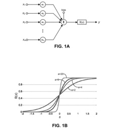
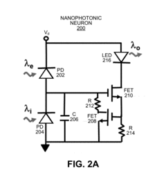
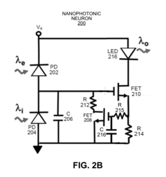
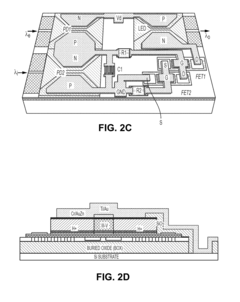
- A photonic neuron system is designed with excitatory and inhibitory input detectors, an electrical neuron for integrating signals, and a light-emitting output device, implemented in a 3D integrated neuromorphic computing system using nanophotonic neural networks and optical interconnection networks with Mach-Zehnder interferometer blocks, enabling efficient energy use and scalability.
Energy Efficiency Standards for Photonic Computing Systems
The establishment of comprehensive energy efficiency standards for photonic computing systems represents a critical milestone in the development of neuromorphic photonic computing for natural language processing applications. Current industry initiatives focus on defining standardized metrics that encompass both static and dynamic power consumption patterns, with particular emphasis on photonic-electronic interface efficiency and optical signal processing overhead.
Emerging standards frameworks prioritize the development of unified measurement protocols for evaluating energy consumption across different operational modes. These protocols address the unique characteristics of photonic systems, including laser source efficiency, optical modulator power requirements, and photodetector sensitivity thresholds. The standards specifically target neuromorphic architectures where spike-based processing demands highly variable power profiles compared to traditional digital systems.
International standardization bodies are collaborating to establish baseline energy efficiency benchmarks that account for the inherent advantages of photonic computing in parallel processing scenarios. These benchmarks incorporate wavelength division multiplexing efficiency, optical interconnect losses, and thermal management requirements specific to high-speed natural language processing workloads.
The proposed standards framework introduces tiered efficiency classifications based on computational throughput per watt metrics, enabling fair comparison between different neuromorphic photonic architectures. Special consideration is given to burst processing capabilities essential for real-time language understanding tasks, where instantaneous power spikes must be balanced against average consumption levels.
Compliance verification procedures are being developed to ensure consistent implementation across various photonic computing platforms. These procedures include standardized testing methodologies for measuring end-to-end system efficiency, from optical input processing through neural network computation to final output generation. The standards also address cooling system integration and ambient temperature operational requirements.
Future revisions of these energy efficiency standards will incorporate adaptive power management protocols specifically designed for neuromorphic photonic systems, enabling dynamic optimization based on workload characteristics and real-time performance requirements in natural language processing applications.
Emerging standards frameworks prioritize the development of unified measurement protocols for evaluating energy consumption across different operational modes. These protocols address the unique characteristics of photonic systems, including laser source efficiency, optical modulator power requirements, and photodetector sensitivity thresholds. The standards specifically target neuromorphic architectures where spike-based processing demands highly variable power profiles compared to traditional digital systems.
International standardization bodies are collaborating to establish baseline energy efficiency benchmarks that account for the inherent advantages of photonic computing in parallel processing scenarios. These benchmarks incorporate wavelength division multiplexing efficiency, optical interconnect losses, and thermal management requirements specific to high-speed natural language processing workloads.
The proposed standards framework introduces tiered efficiency classifications based on computational throughput per watt metrics, enabling fair comparison between different neuromorphic photonic architectures. Special consideration is given to burst processing capabilities essential for real-time language understanding tasks, where instantaneous power spikes must be balanced against average consumption levels.
Compliance verification procedures are being developed to ensure consistent implementation across various photonic computing platforms. These procedures include standardized testing methodologies for measuring end-to-end system efficiency, from optical input processing through neural network computation to final output generation. The standards also address cooling system integration and ambient temperature operational requirements.
Future revisions of these energy efficiency standards will incorporate adaptive power management protocols specifically designed for neuromorphic photonic systems, enabling dynamic optimization based on workload characteristics and real-time performance requirements in natural language processing applications.
Scalability Challenges in Neuromorphic Photonic Fabrication
The fabrication of neuromorphic photonic devices for natural language processing applications faces significant scalability challenges that currently limit widespread commercial deployment. Manufacturing precision requirements for photonic neural networks demand nanometer-scale accuracy in waveguide dimensions, coupling efficiencies, and optical path lengths. Current lithographic techniques struggle to maintain consistent performance across large-scale wafer production, with yield rates typically falling below 60% for complex neuromorphic photonic circuits containing thousands of interconnected components.
Process variability represents a critical bottleneck in scaling neuromorphic photonic fabrication. Silicon photonic platforms require precise control of layer thickness variations, typically within ±2 nanometers, to ensure uniform optical properties across entire wafers. Temperature fluctuations during fabrication can introduce phase mismatches that severely degrade the computational accuracy of neuromorphic networks. These variations become exponentially more problematic as device complexity increases, making it challenging to fabricate large-scale arrays of photonic neurons and synapses with consistent performance characteristics.
Integration complexity poses another fundamental scalability barrier. Neuromorphic photonic systems require seamless integration of multiple material platforms, including silicon photonics, III-V semiconductors for optical gain, and specialized nonlinear optical materials for synaptic functionality. Current heterogeneous integration techniques involve multiple bonding and transfer processes that introduce defects and reduce overall device reliability. The alignment tolerances between different material layers often exceed manufacturing capabilities when scaling to wafer-level production.
Cost considerations further compound scalability challenges in neuromorphic photonic fabrication. The specialized equipment required for precise optical component manufacturing represents substantial capital investments that are difficult to justify without guaranteed high-volume production. Current fabrication costs per neuromorphic photonic chip remain orders of magnitude higher than equivalent electronic processors, primarily due to low yield rates and complex multi-step processing requirements.
Standardization gaps in neuromorphic photonic fabrication processes hinder industry-wide scaling efforts. Unlike mature semiconductor manufacturing, neuromorphic photonics lacks established design rules, testing protocols, and quality control standards. This absence of standardization makes it difficult for multiple foundries to produce compatible devices, limiting the development of a robust supply chain necessary for large-scale deployment in natural language processing applications.
Process variability represents a critical bottleneck in scaling neuromorphic photonic fabrication. Silicon photonic platforms require precise control of layer thickness variations, typically within ±2 nanometers, to ensure uniform optical properties across entire wafers. Temperature fluctuations during fabrication can introduce phase mismatches that severely degrade the computational accuracy of neuromorphic networks. These variations become exponentially more problematic as device complexity increases, making it challenging to fabricate large-scale arrays of photonic neurons and synapses with consistent performance characteristics.
Integration complexity poses another fundamental scalability barrier. Neuromorphic photonic systems require seamless integration of multiple material platforms, including silicon photonics, III-V semiconductors for optical gain, and specialized nonlinear optical materials for synaptic functionality. Current heterogeneous integration techniques involve multiple bonding and transfer processes that introduce defects and reduce overall device reliability. The alignment tolerances between different material layers often exceed manufacturing capabilities when scaling to wafer-level production.
Cost considerations further compound scalability challenges in neuromorphic photonic fabrication. The specialized equipment required for precise optical component manufacturing represents substantial capital investments that are difficult to justify without guaranteed high-volume production. Current fabrication costs per neuromorphic photonic chip remain orders of magnitude higher than equivalent electronic processors, primarily due to low yield rates and complex multi-step processing requirements.
Standardization gaps in neuromorphic photonic fabrication processes hinder industry-wide scaling efforts. Unlike mature semiconductor manufacturing, neuromorphic photonics lacks established design rules, testing protocols, and quality control standards. This absence of standardization makes it difficult for multiple foundries to produce compatible devices, limiting the development of a robust supply chain necessary for large-scale deployment in natural language processing applications.
Unlock deeper insights with PatSnap Eureka Quick Research — get a full tech report to explore trends and direct your research. Try now!
Generate Your Research Report Instantly with AI Agent
Supercharge your innovation with PatSnap Eureka AI Agent Platform!