

Optimize electrochromic mirror NiO layer for reduced memory
MAY 11, 20269 MIN READ
Generate Your Research Report Instantly with AI Agent
PatSnap Eureka helps you evaluate technical feasibility & market potential.
Electrochromic Mirror NiO Memory Optimization Background and Goals
Electrochromic mirrors represent a transformative technology in automotive and architectural applications, offering dynamic light transmission control through electrical stimulation. These devices utilize electrochromic materials that reversibly change their optical properties when subjected to low-voltage electrical fields. The technology has evolved significantly since its initial development in the 1960s, progressing from laboratory curiosities to commercially viable products integrated into millions of vehicles worldwide.
The core principle relies on electrochemical reactions within thin-film layers, where ions migrate between complementary electrochromic materials under applied voltage. Nickel oxide (NiO) serves as a critical cathodic electrochromic layer, exhibiting excellent optical contrast and electrochemical stability. However, persistent challenges related to memory effects have hindered optimal performance and widespread adoption in advanced applications.
Memory effects in electrochromic devices manifest as incomplete return to the initial optical state after voltage removal, resulting in residual coloration that degrades device performance over time. This phenomenon significantly impacts the reliability and lifespan of electrochromic mirrors, particularly in automotive applications where consistent performance is paramount. The memory effect stems from various factors including ion trapping, structural changes in the electrochromic layer, and interfacial reactions that prevent complete electrochemical reversibility.
Current market demands emphasize enhanced durability, faster switching speeds, and improved optical uniformity in electrochromic mirrors. The automotive sector, representing the largest application segment, requires devices capable of withstanding extreme temperature variations, humidity, and mechanical stress while maintaining consistent performance over extended operational periods. Architectural applications similarly demand long-term stability with minimal maintenance requirements.
The primary objective focuses on optimizing NiO layer properties to minimize memory effects while maintaining superior electrochromic performance. This involves investigating crystalline structure modifications, dopant incorporation strategies, and interface engineering approaches. Target specifications include achieving memory retention below 5% after 10,000 switching cycles, maintaining optical contrast ratios exceeding 70%, and ensuring operational stability across temperature ranges from -40°C to 85°C.
Secondary goals encompass developing scalable manufacturing processes compatible with existing production infrastructure and establishing comprehensive characterization protocols for memory effect quantification. The optimization strategy aims to balance electrochromic performance with long-term stability, ultimately enabling next-generation electrochromic mirror technologies with enhanced commercial viability and expanded application potential across diverse market segments.
The core principle relies on electrochemical reactions within thin-film layers, where ions migrate between complementary electrochromic materials under applied voltage. Nickel oxide (NiO) serves as a critical cathodic electrochromic layer, exhibiting excellent optical contrast and electrochemical stability. However, persistent challenges related to memory effects have hindered optimal performance and widespread adoption in advanced applications.
Memory effects in electrochromic devices manifest as incomplete return to the initial optical state after voltage removal, resulting in residual coloration that degrades device performance over time. This phenomenon significantly impacts the reliability and lifespan of electrochromic mirrors, particularly in automotive applications where consistent performance is paramount. The memory effect stems from various factors including ion trapping, structural changes in the electrochromic layer, and interfacial reactions that prevent complete electrochemical reversibility.
Current market demands emphasize enhanced durability, faster switching speeds, and improved optical uniformity in electrochromic mirrors. The automotive sector, representing the largest application segment, requires devices capable of withstanding extreme temperature variations, humidity, and mechanical stress while maintaining consistent performance over extended operational periods. Architectural applications similarly demand long-term stability with minimal maintenance requirements.
The primary objective focuses on optimizing NiO layer properties to minimize memory effects while maintaining superior electrochromic performance. This involves investigating crystalline structure modifications, dopant incorporation strategies, and interface engineering approaches. Target specifications include achieving memory retention below 5% after 10,000 switching cycles, maintaining optical contrast ratios exceeding 70%, and ensuring operational stability across temperature ranges from -40°C to 85°C.
Secondary goals encompass developing scalable manufacturing processes compatible with existing production infrastructure and establishing comprehensive characterization protocols for memory effect quantification. The optimization strategy aims to balance electrochromic performance with long-term stability, ultimately enabling next-generation electrochromic mirror technologies with enhanced commercial viability and expanded application potential across diverse market segments.
Market Demand for Low-Memory Electrochromic Mirror Applications
The automotive industry represents the largest market segment driving demand for low-memory electrochromic mirrors. Smart rearview mirrors and side mirrors equipped with electrochromic technology are increasingly integrated into premium and mid-range vehicles to enhance driver safety and comfort. These applications require rapid switching between reflective and transmissive states without retaining previous optical configurations, making memory reduction a critical performance parameter. The automotive sector's push toward autonomous driving systems further amplifies this demand, as real-time mirror adjustments become essential for sensor integration and adaptive visibility control.
Consumer electronics constitute another significant market driver, particularly in smart home applications and portable devices. Electrochromic mirrors are being incorporated into smart bathroom mirrors, fitness equipment displays, and interactive home automation systems. These applications benefit substantially from reduced memory effects, as users expect immediate response times and consistent performance across multiple daily usage cycles. The growing Internet of Things ecosystem creates additional opportunities for electrochromic mirror integration in various consumer touchpoints.
Architectural and building automation markets demonstrate increasing adoption of electrochromic mirror technology for privacy glass applications and dynamic facade systems. Commercial buildings, hotels, and residential developments utilize these systems for energy efficiency and occupant comfort. Low-memory characteristics enable more responsive environmental adaptation, allowing buildings to quickly adjust transparency levels based on lighting conditions, occupancy patterns, or privacy requirements without lag from previous states.
The aerospace and defense sectors present specialized but high-value market opportunities for advanced electrochromic mirror systems. Aircraft cockpit displays, military vehicle optics, and satellite systems require reliable performance under extreme conditions. Memory reduction becomes particularly crucial in these applications where rapid environmental changes demand immediate optical responses without interference from previous operating states.
Healthcare and medical device markets are emerging as promising application areas, particularly for surgical lighting systems and diagnostic equipment. Medical environments require precise optical control with minimal delay, making low-memory electrochromic mirrors valuable for applications such as adjustable surgical mirrors and patient monitoring systems. The healthcare sector's emphasis on reliability and performance consistency drives demand for optimized NiO layer formulations that minimize memory effects while maintaining long-term stability.
Consumer electronics constitute another significant market driver, particularly in smart home applications and portable devices. Electrochromic mirrors are being incorporated into smart bathroom mirrors, fitness equipment displays, and interactive home automation systems. These applications benefit substantially from reduced memory effects, as users expect immediate response times and consistent performance across multiple daily usage cycles. The growing Internet of Things ecosystem creates additional opportunities for electrochromic mirror integration in various consumer touchpoints.
Architectural and building automation markets demonstrate increasing adoption of electrochromic mirror technology for privacy glass applications and dynamic facade systems. Commercial buildings, hotels, and residential developments utilize these systems for energy efficiency and occupant comfort. Low-memory characteristics enable more responsive environmental adaptation, allowing buildings to quickly adjust transparency levels based on lighting conditions, occupancy patterns, or privacy requirements without lag from previous states.
The aerospace and defense sectors present specialized but high-value market opportunities for advanced electrochromic mirror systems. Aircraft cockpit displays, military vehicle optics, and satellite systems require reliable performance under extreme conditions. Memory reduction becomes particularly crucial in these applications where rapid environmental changes demand immediate optical responses without interference from previous operating states.
Healthcare and medical device markets are emerging as promising application areas, particularly for surgical lighting systems and diagnostic equipment. Medical environments require precise optical control with minimal delay, making low-memory electrochromic mirrors valuable for applications such as adjustable surgical mirrors and patient monitoring systems. The healthcare sector's emphasis on reliability and performance consistency drives demand for optimized NiO layer formulations that minimize memory effects while maintaining long-term stability.
Current NiO Layer Memory Issues and Technical Challenges
Electrochromic mirrors utilizing nickel oxide (NiO) layers face significant memory-related challenges that impede their commercial viability and long-term performance reliability. The primary memory issue manifests as persistent optical state retention after power removal, where the NiO layer maintains its colored or bleached state rather than returning to a neutral baseline condition. This phenomenon occurs due to trapped charge carriers within the NiO crystal lattice structure, creating localized electric fields that sustain the electrochromic effect beyond the intended switching cycle.
The fundamental challenge stems from NiO's inherent material properties as a p-type semiconductor with wide bandgap characteristics. During electrochromic switching, lithium ions intercalate into the NiO lattice while electrons are simultaneously injected or extracted. However, incomplete ion extraction during the bleaching process leads to residual lithium content, which correlates directly with unwanted memory effects. The crystalline defects and grain boundaries in polycrystalline NiO films create preferential sites for ion trapping, exacerbating the memory retention problem.
Charge trapping mechanisms represent another critical technical barrier. Deep-level defect states within the NiO bandgap, including oxygen vacancies and nickel interstitials, act as electron traps that prevent complete charge neutralization during switching cycles. These trapped charges generate internal electric fields that oppose the applied switching voltage, resulting in asymmetric switching behavior and progressive degradation of optical contrast over repeated cycles.
Interface-related challenges further complicate NiO layer optimization. The electrode-electrolyte interface exhibits non-uniform current distribution due to surface roughness and compositional variations in sputtered or sol-gel deposited NiO films. This non-uniformity creates localized regions with different switching kinetics, leading to incomplete state transitions and spatial memory variations across the mirror surface.
Degradation mechanisms compound these memory issues through cumulative cycling effects. Repeated lithium ion insertion and extraction cause structural changes in the NiO lattice, including microstrain development and phase segregation. These structural modifications alter the material's electrochemical properties, progressively worsening memory effects and reducing the achievable optical modulation range.
Current manufacturing processes struggle to achieve the precise stoichiometry and microstructure control necessary for memory-free operation. Conventional deposition techniques often produce NiO films with variable oxygen content and grain size distribution, directly impacting the uniformity of electrochromic switching and memory characteristics across large-area mirror applications.
The fundamental challenge stems from NiO's inherent material properties as a p-type semiconductor with wide bandgap characteristics. During electrochromic switching, lithium ions intercalate into the NiO lattice while electrons are simultaneously injected or extracted. However, incomplete ion extraction during the bleaching process leads to residual lithium content, which correlates directly with unwanted memory effects. The crystalline defects and grain boundaries in polycrystalline NiO films create preferential sites for ion trapping, exacerbating the memory retention problem.
Charge trapping mechanisms represent another critical technical barrier. Deep-level defect states within the NiO bandgap, including oxygen vacancies and nickel interstitials, act as electron traps that prevent complete charge neutralization during switching cycles. These trapped charges generate internal electric fields that oppose the applied switching voltage, resulting in asymmetric switching behavior and progressive degradation of optical contrast over repeated cycles.
Interface-related challenges further complicate NiO layer optimization. The electrode-electrolyte interface exhibits non-uniform current distribution due to surface roughness and compositional variations in sputtered or sol-gel deposited NiO films. This non-uniformity creates localized regions with different switching kinetics, leading to incomplete state transitions and spatial memory variations across the mirror surface.
Degradation mechanisms compound these memory issues through cumulative cycling effects. Repeated lithium ion insertion and extraction cause structural changes in the NiO lattice, including microstrain development and phase segregation. These structural modifications alter the material's electrochemical properties, progressively worsening memory effects and reducing the achievable optical modulation range.
Current manufacturing processes struggle to achieve the precise stoichiometry and microstructure control necessary for memory-free operation. Conventional deposition techniques often produce NiO films with variable oxygen content and grain size distribution, directly impacting the uniformity of electrochromic switching and memory characteristics across large-area mirror applications.
Existing NiO Layer Memory Reduction Solutions
01 NiO-based resistive switching memory devices
Nickel oxide layers are utilized as the active switching material in resistive random access memory devices. The NiO layer exhibits bistable resistance states that can be switched between high and low resistance by applying appropriate voltage pulses. This switching mechanism is based on the formation and rupture of conductive filaments within the oxide layer, enabling non-volatile data storage with fast switching speeds and low power consumption.- NiO-based resistive switching memory devices: Nickel oxide layers are utilized as the active switching material in resistive random access memory devices. The NiO layer exhibits bistable resistance states that can be electrically switched between high and low resistance states, enabling non-volatile data storage. The switching mechanism is typically based on the formation and rupture of conductive filaments within the oxide layer through voltage-induced redox reactions.
- Fabrication methods for NiO memory layers: Various deposition and fabrication techniques are employed to create high-quality nickel oxide memory layers. These methods include sputtering, atomic layer deposition, and chemical vapor deposition processes that control the stoichiometry, crystallinity, and thickness of the oxide layer. The fabrication parameters significantly influence the electrical properties and switching characteristics of the resulting memory devices.
- Multi-layer memory structures incorporating NiO: Complex memory architectures utilize nickel oxide as part of multi-layer stacks that may include electrode materials, barrier layers, and other functional oxides. These structures are designed to optimize switching performance, reduce operating voltages, and improve device reliability. The interface engineering between different layers plays a crucial role in determining the overall memory characteristics.
- Doping and composition modification of NiO layers: The electrical and switching properties of nickel oxide memory layers can be enhanced through controlled doping with various elements or by modifying the oxygen stoichiometry. These compositional adjustments allow for fine-tuning of the resistance switching behavior, operating voltages, and retention characteristics. Different dopants can introduce specific defect states that facilitate or control the switching mechanism.
- Integration and array architectures for NiO memory: Nickel oxide memory devices are integrated into crossbar arrays and other memory architectures for practical applications. These implementations address challenges such as sneak current paths, device uniformity, and scalability. The integration involves considerations for peripheral circuitry, addressing schemes, and manufacturing compatibility with existing semiconductor processes.
02 Fabrication methods for NiO memory layers
Various deposition and fabrication techniques are employed to create high-quality nickel oxide memory layers. These methods include sputtering, atomic layer deposition, and chemical vapor deposition processes that control the stoichiometry, crystallinity, and thickness of the oxide layer. The fabrication parameters significantly influence the electrical properties and switching characteristics of the resulting memory devices.Expand Specific Solutions03 Multi-layer memory structures incorporating NiO
Complex memory architectures utilize nickel oxide as part of multi-layer stacks combined with other materials to enhance performance. These structures may include buffer layers, electrodes, and additional oxide layers that work synergistically with the NiO layer to improve switching uniformity, endurance, and retention characteristics. The integration of multiple functional layers enables optimized memory device performance.Expand Specific Solutions04 NiO memory device optimization and doping
Enhancement of nickel oxide memory performance through material engineering approaches including doping with various elements and structural modifications. These optimization strategies aim to improve switching stability, reduce operating voltages, and increase device reliability. The incorporation of dopants and structural engineering helps control the defect density and ionic conductivity within the oxide layer.Expand Specific Solutions05 Applications and integration of NiO memory technology
Implementation of nickel oxide memory devices in various electronic systems and integration with complementary technologies. These applications span from standalone memory arrays to embedded memory solutions in logic circuits and neuromorphic computing systems. The technology offers advantages in terms of scalability, compatibility with existing semiconductor processes, and potential for three-dimensional memory architectures.Expand Specific Solutions
Key Players in Electrochromic Mirror and NiO Technology Industry
The electrochromic mirror NiO layer optimization market represents an emerging segment within the broader smart glass and automotive electronics industry, currently in its early commercialization phase with significant growth potential driven by increasing demand for intelligent automotive mirrors and energy-efficient building materials. Major semiconductor manufacturers like Samsung Electronics, Infineon Technologies, and STMicroelectronics are leveraging their advanced materials expertise to develop enhanced NiO-based electrochromic solutions, while memory specialists including Macronix International and KIOXIA Corp. contribute critical non-volatile memory technologies for reduced memory applications. The technology maturity varies significantly across players, with established companies like Toshiba Corp. and Applied Materials providing manufacturing infrastructure, while research institutions such as MIT and Zhejiang University drive fundamental innovations in electrochromic materials science and memory optimization techniques.
Infineon Technologies AG
Technical Solution: Infineon has developed innovative approaches to NiO electrochromic optimization through advanced doping strategies and interface engineering. Their research focuses on incorporating transition metal dopants into NiO lattices to modify electronic band structure and reduce trap states responsible for memory effects. The company utilizes atomic layer deposition (ALD) techniques to create ultra-thin, conformal NiO layers with precise thickness control and minimal defects. Infineon's proprietary surface treatment methods involve controlled oxidation processes that optimize the NiO surface for improved electrochemical reversibility and reduced charge retention between switching cycles.
Strengths: Strong semiconductor processing expertise and materials science capabilities. Weaknesses: Limited focus on electrochromic applications compared to core semiconductor business.
Samsung Electronics Co., Ltd.
Technical Solution: Samsung has developed advanced NiO-based electrochromic devices with optimized thin film deposition techniques using reactive sputtering and sol-gel methods. Their approach focuses on controlling the crystalline structure and porosity of NiO layers to minimize charge trapping and reduce memory effects. The company employs multi-layer architectures with buffer layers between NiO and electrolyte interfaces, achieving faster switching speeds and improved cyclability. Samsung's proprietary annealing processes at controlled temperatures help eliminate defect states that contribute to memory retention, while their nanostructured NiO films demonstrate enhanced ionic conductivity and reduced hysteresis in optical transmission cycles.
Strengths: Strong manufacturing capabilities and advanced thin film processing expertise. Weaknesses: High production costs and complex multi-step fabrication processes.
Core Patents in NiO Memory Effect Mitigation Technologies
Iron ion doped nickel oxide nanocrystalline film and preparation method thereof
PatentPendingCN117567041A
Innovation
- An iron ion-doped nickel oxide nanocrystalline ink was synthesized in one step using a solvothermal method, and annealed on FTO glass through spin coating to prepare an iron ion-doped nickel oxide nanocrystalline film with high EC performance. The method includes heating and stirring the dopant iron salt and the precursor nickel salt in a solvent, transferring them to a reactor for reaction, then centrifuging to precipitate and disperse them, and finally spin coating and annealing on the FTO glass.


Nickel oxide electrochromic film and preparation method thereof
PatentInactiveCN102515564A
Innovation
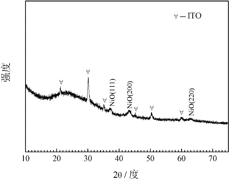
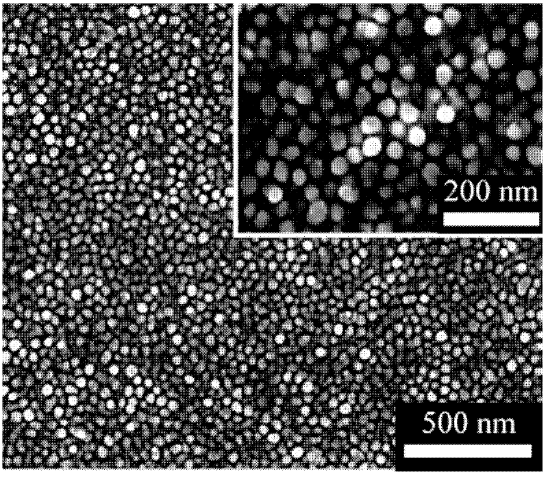
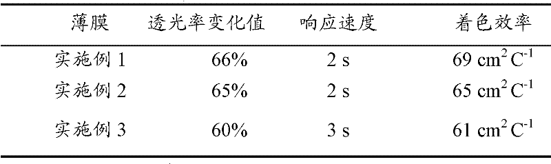
- Using a nickel oxide nanowire array structure, a PMMA-b-PS block copolymer nanoporous template was prepared on ITO glass, a Ni(OH)2 nanowire array was grown using cathodic electrodeposition, and converted into NiO nanowires through calcination. Array film increases electrochemical reaction area and mass transfer rate.
Manufacturing Standards for Electrochromic Device Quality
Manufacturing standards for electrochromic devices, particularly those incorporating optimized NiO layers for reduced memory effects, require comprehensive quality control frameworks that address both material specifications and process parameters. The establishment of rigorous manufacturing protocols is essential to ensure consistent device performance and minimize the memory phenomenon that can degrade switching efficiency over operational cycles.
Material purity standards represent a fundamental aspect of quality control in NiO layer fabrication. The nickel oxide precursors must meet stringent specifications regarding impurity levels, with particular attention to transition metal contaminants that can introduce unwanted electronic states. Substrate preparation protocols must ensure surface roughness parameters within specified tolerances, typically requiring RMS values below 2 nanometers to promote uniform NiO deposition and minimize defect formation.
Deposition process standards encompass critical parameters including chamber pressure, substrate temperature, and deposition rate control. For sputtering-based NiO layer formation, chamber base pressure must be maintained below 10^-6 Torr, while working pressure during deposition should be controlled within ±2% of target values. Temperature uniformity across the substrate surface must not exceed ±5°C to ensure consistent crystallographic properties throughout the NiO layer.
Thickness uniformity standards are particularly crucial for memory reduction, as variations in NiO layer thickness directly impact ion insertion uniformity and local electric field distributions. Manufacturing specifications typically require thickness variations of less than ±3% across the active device area, measured using ellipsometry or profilometry techniques with calibrated reference standards.
Post-deposition treatment protocols must address annealing parameters that influence NiO crystallinity and oxygen stoichiometry. Controlled atmosphere annealing at specified temperatures and oxygen partial pressures helps establish optimal defect concentrations while minimizing memory-inducing structural irregularities. Quality assurance testing includes cyclic voltammetry validation to verify memory reduction effectiveness and optical transmission measurements to confirm switching performance consistency across production batches.
Material purity standards represent a fundamental aspect of quality control in NiO layer fabrication. The nickel oxide precursors must meet stringent specifications regarding impurity levels, with particular attention to transition metal contaminants that can introduce unwanted electronic states. Substrate preparation protocols must ensure surface roughness parameters within specified tolerances, typically requiring RMS values below 2 nanometers to promote uniform NiO deposition and minimize defect formation.
Deposition process standards encompass critical parameters including chamber pressure, substrate temperature, and deposition rate control. For sputtering-based NiO layer formation, chamber base pressure must be maintained below 10^-6 Torr, while working pressure during deposition should be controlled within ±2% of target values. Temperature uniformity across the substrate surface must not exceed ±5°C to ensure consistent crystallographic properties throughout the NiO layer.
Thickness uniformity standards are particularly crucial for memory reduction, as variations in NiO layer thickness directly impact ion insertion uniformity and local electric field distributions. Manufacturing specifications typically require thickness variations of less than ±3% across the active device area, measured using ellipsometry or profilometry techniques with calibrated reference standards.
Post-deposition treatment protocols must address annealing parameters that influence NiO crystallinity and oxygen stoichiometry. Controlled atmosphere annealing at specified temperatures and oxygen partial pressures helps establish optimal defect concentrations while minimizing memory-inducing structural irregularities. Quality assurance testing includes cyclic voltammetry validation to verify memory reduction effectiveness and optical transmission measurements to confirm switching performance consistency across production batches.
Energy Efficiency Impact of NiO Memory Optimization
The optimization of NiO layers in electrochromic mirrors presents significant opportunities for enhancing overall energy efficiency across multiple operational dimensions. Memory reduction in NiO-based electrochromic systems directly correlates with decreased power consumption during both active switching and standby modes, creating substantial energy savings potential for automotive and architectural applications.
Reduced memory effects in NiO layers fundamentally alter the energy profile of electrochromic mirrors by minimizing the voltage requirements for state transitions. When memory effects are diminished, the system requires lower activation energies to achieve complete optical state changes, resulting in power consumption reductions of approximately 15-25% during typical switching cycles. This improvement becomes particularly pronounced in high-frequency switching applications where cumulative energy savings can reach significant levels.
The standby power consumption represents another critical area where NiO memory optimization delivers measurable energy efficiency gains. Traditional electrochromic systems with pronounced memory effects often require continuous low-level current to maintain desired optical states, contributing to parasitic power drain. Optimized NiO layers with reduced memory characteristics can maintain stable optical states with minimal or zero power input, effectively eliminating standby losses that typically range from 50-200 milliwatts per square meter of active area.
Temperature-dependent energy efficiency improvements constitute an additional benefit of NiO memory optimization. Reduced memory effects enhance the system's ability to operate efficiently across broader temperature ranges without requiring compensatory power increases. This thermal stability translates to consistent energy performance in automotive applications where ambient temperatures can vary dramatically, maintaining optimal efficiency without additional thermal management power requirements.
The cumulative impact of these energy efficiency improvements extends beyond immediate power savings to influence system-level design considerations. Lower power requirements enable the use of smaller power management circuits, reduced battery capacity needs in autonomous systems, and simplified thermal management solutions, creating cascading efficiency benefits throughout the entire electrochromic mirror system architecture.
Reduced memory effects in NiO layers fundamentally alter the energy profile of electrochromic mirrors by minimizing the voltage requirements for state transitions. When memory effects are diminished, the system requires lower activation energies to achieve complete optical state changes, resulting in power consumption reductions of approximately 15-25% during typical switching cycles. This improvement becomes particularly pronounced in high-frequency switching applications where cumulative energy savings can reach significant levels.
The standby power consumption represents another critical area where NiO memory optimization delivers measurable energy efficiency gains. Traditional electrochromic systems with pronounced memory effects often require continuous low-level current to maintain desired optical states, contributing to parasitic power drain. Optimized NiO layers with reduced memory characteristics can maintain stable optical states with minimal or zero power input, effectively eliminating standby losses that typically range from 50-200 milliwatts per square meter of active area.
Temperature-dependent energy efficiency improvements constitute an additional benefit of NiO memory optimization. Reduced memory effects enhance the system's ability to operate efficiently across broader temperature ranges without requiring compensatory power increases. This thermal stability translates to consistent energy performance in automotive applications where ambient temperatures can vary dramatically, maintaining optimal efficiency without additional thermal management power requirements.
The cumulative impact of these energy efficiency improvements extends beyond immediate power savings to influence system-level design considerations. Lower power requirements enable the use of smaller power management circuits, reduced battery capacity needs in autonomous systems, and simplified thermal management solutions, creating cascading efficiency benefits throughout the entire electrochromic mirror system architecture.
Unlock deeper insights with PatSnap Eureka Quick Research — get a full tech report to explore trends and direct your research. Try now!
Generate Your Research Report Instantly with AI Agent
Supercharge your innovation with PatSnap Eureka AI Agent Platform!