Silicon photonics for efficient light manipulation.
JUL 17, 20259 MIN READ
Generate Your Research Report Instantly with AI Agent
Patsnap Eureka helps you evaluate technical feasibility & market potential.
Silicon Photonics Evolution and Objectives
Silicon photonics has emerged as a transformative technology in the field of integrated optics, revolutionizing the way we manipulate and control light at the nanoscale. The evolution of this technology can be traced back to the late 1980s when researchers first explored the potential of using silicon as a platform for photonic devices. Since then, silicon photonics has undergone rapid development, driven by the increasing demand for high-speed data transmission and efficient optical computing.
The primary objective of silicon photonics research is to achieve efficient light manipulation on a silicon-based platform. This goal encompasses several key aspects, including the development of low-loss waveguides, high-performance modulators, and sensitive photodetectors. By leveraging the mature semiconductor manufacturing processes, silicon photonics aims to integrate optical and electronic components on a single chip, enabling unprecedented levels of functionality and performance.
One of the most significant milestones in the evolution of silicon photonics was the demonstration of the first silicon-based laser in 2005. This breakthrough opened up new possibilities for on-chip light sources, a critical component for fully integrated photonic circuits. Subsequently, researchers have made substantial progress in improving the efficiency and reliability of silicon-based optical devices, paving the way for their commercial adoption.
The current landscape of silicon photonics research is characterized by a focus on enhancing the performance of individual components while simultaneously working towards large-scale integration. Key areas of investigation include the development of novel materials and structures to overcome the inherent limitations of silicon, such as its indirect bandgap nature. Additionally, researchers are exploring advanced fabrication techniques to improve device uniformity and yield, crucial factors for mass production.
Looking ahead, the objectives of silicon photonics research are multifaceted. In the short term, efforts are directed towards improving the efficiency and bandwidth of optical interconnects for data centers and high-performance computing applications. The medium-term goals include the development of integrated photonic sensors for applications in healthcare, environmental monitoring, and autonomous vehicles. Long-term objectives encompass the realization of all-optical computing systems and the integration of photonics with emerging technologies such as quantum computing and neuromorphic computing.
As silicon photonics continues to evolve, it holds the promise of enabling a new generation of compact, energy-efficient, and high-performance devices. The ongoing research in this field is not only pushing the boundaries of what is possible in light manipulation but also paving the way for revolutionary applications across various industries. The convergence of silicon photonics with other cutting-edge technologies is expected to drive innovation and create new paradigms in information processing and communication in the coming decades.
Market Demand for Integrated Photonics
The market demand for integrated photonics, particularly in the realm of silicon photonics for efficient light manipulation, has been experiencing significant growth in recent years. This surge is primarily driven by the increasing need for high-speed data transmission, energy-efficient computing, and advanced sensing technologies across various industries.
In the telecommunications sector, the demand for silicon photonics is particularly strong. As global internet traffic continues to grow exponentially, there is a pressing need for higher bandwidth and more energy-efficient data transmission solutions. Silicon photonics offers the potential to meet these requirements by enabling faster data transfer rates and reducing power consumption in optical communication systems.
The data center industry is another major driver of market demand for integrated photonics. With the rapid expansion of cloud computing and big data analytics, data centers are constantly seeking ways to improve their performance and energy efficiency. Silicon photonics technology can provide significant advantages in terms of data transfer speeds, power consumption, and heat dissipation, making it an attractive solution for next-generation data center architectures.
In the field of high-performance computing, there is growing interest in using silicon photonics for chip-to-chip and intra-chip communication. This technology has the potential to overcome the limitations of traditional electronic interconnects, offering higher bandwidth and lower latency for advanced computing systems.
The automotive industry is also showing increased demand for integrated photonics, particularly in the development of LiDAR (Light Detection and Ranging) systems for autonomous vehicles. Silicon photonics can enable more compact, cost-effective, and high-performance LiDAR solutions, which are crucial for the widespread adoption of self-driving cars.
In the healthcare sector, there is a growing market for silicon photonics in medical imaging and diagnostic devices. The technology's ability to manipulate light efficiently opens up new possibilities for non-invasive imaging techniques and point-of-care diagnostic tools.
The aerospace and defense industries are also driving demand for integrated photonics, with applications in advanced sensing, secure communications, and high-performance computing for mission-critical systems.
As the technology matures and manufacturing processes improve, the market for silicon photonics is expected to expand further. This growth is likely to be fueled by emerging applications in quantum computing, artificial intelligence, and 5G/6G communications, where efficient light manipulation will play a crucial role in enabling next-generation technologies.
Current Challenges in Silicon Photonics
Silicon photonics has emerged as a promising technology for efficient light manipulation, offering potential solutions for high-speed data transmission and processing. However, several significant challenges currently hinder its widespread adoption and full realization of its potential.
One of the primary challenges in silicon photonics is the efficient coupling of light between optical fibers and silicon waveguides. The substantial size mismatch between these components leads to significant coupling losses, reducing overall system efficiency. Various approaches, such as grating couplers and edge couplers, have been developed to address this issue, but further improvements in coupling efficiency and bandwidth are still required.
Another critical challenge is the development of efficient, compact, and low-power modulators. While silicon-based modulators have shown promise, they often suffer from limited modulation speed, high power consumption, or large footprints. Researchers are exploring novel materials and structures, including hybrid silicon-organic modulators and plasmonic modulators, to overcome these limitations and achieve higher modulation speeds with reduced energy consumption.
The integration of light sources on silicon platforms remains a significant hurdle. Silicon's indirect bandgap makes it an inefficient light emitter, necessitating the integration of III-V materials or other light-emitting components. While hybrid integration approaches have shown progress, challenges persist in terms of thermal management, coupling efficiency, and large-scale manufacturing.
Polarization management is another crucial challenge in silicon photonics. The high index contrast in silicon waveguides leads to strong polarization dependence, which can affect device performance and system reliability. Developing polarization-insensitive or polarization-diverse components is essential for robust and versatile photonic integrated circuits.
Thermal management and athermal design pose significant challenges in silicon photonics. The high thermo-optic coefficient of silicon makes devices sensitive to temperature fluctuations, affecting their performance and reliability. Implementing effective thermal management strategies and developing athermal designs are crucial for stable operation across varying environmental conditions.
Lastly, the development of efficient and scalable packaging solutions remains a challenge. Integrating photonic chips with electronic components, ensuring proper thermal management, and providing robust fiber-to-chip coupling in a cost-effective manner are critical for the commercial viability of silicon photonic systems.
Addressing these challenges requires interdisciplinary research efforts, combining expertise in materials science, device physics, circuit design, and manufacturing processes. Overcoming these hurdles will pave the way for the widespread adoption of silicon photonics in various applications, including high-speed data centers, telecommunications, and sensing systems.
Existing Silicon Photonics Solutions
01 Waveguide design for light manipulation
Advanced waveguide designs are crucial for efficient light manipulation in silicon photonics. These designs include optimized geometries, materials, and structures to guide and control light propagation. Techniques such as photonic crystals, subwavelength gratings, and metamaterials are employed to enhance light confinement and reduce losses, thereby improving overall efficiency.- Waveguide design for light manipulation: Advanced waveguide designs are crucial for efficient light manipulation in silicon photonics. These designs include optimized geometries, materials, and structures to guide and control light propagation. Techniques such as photonic crystal waveguides, slot waveguides, and subwavelength gratings are employed to enhance light confinement and reduce losses, thereby improving overall efficiency.
- Integration of active and passive components: Efficient light manipulation in silicon photonics relies on the seamless integration of active and passive components. This includes the incorporation of lasers, modulators, detectors, and other optical elements on a single chip. Advanced fabrication techniques and novel materials are used to achieve high-performance integrated photonic circuits with improved light manipulation capabilities.
- Optical coupling and mode conversion: Enhancing coupling efficiency between different optical components and converting between various optical modes are critical for improving light manipulation in silicon photonics. Techniques such as grating couplers, tapered waveguides, and mode converters are employed to minimize coupling losses and ensure efficient light transfer between different parts of the photonic circuit.
- Nonlinear optical effects for light control: Utilizing nonlinear optical effects in silicon and other materials enables advanced light manipulation capabilities. This includes techniques such as four-wave mixing, stimulated Raman scattering, and optical parametric amplification. These nonlinear effects are harnessed to achieve functions like wavelength conversion, signal amplification, and all-optical switching, enhancing the versatility and efficiency of silicon photonic devices.
- Thermal and electrical control for tuning: Implementing thermal and electrical control mechanisms allows for dynamic tuning of optical properties in silicon photonic devices. This includes the use of thermo-optic and electro-optic effects to adjust refractive indices, resonant frequencies, and phase relationships. Such tuning capabilities enable adaptive light manipulation, improving the flexibility and efficiency of silicon photonic systems in various applications.
02 Integration of active and passive components
Efficient light manipulation in silicon photonics relies on the seamless integration of active and passive components. This includes the incorporation of lasers, modulators, detectors, and other optical elements on a single chip. Advanced fabrication techniques and novel materials are used to achieve high-performance integrated photonic circuits with improved light manipulation capabilities.Expand Specific Solutions03 Nanophotonic structures for light control
Nanophotonic structures play a crucial role in enhancing light manipulation efficiency. These include nanoparticles, nanoantennas, and plasmonic structures that can concentrate, redirect, and amplify light at the nanoscale. By leveraging these structures, silicon photonic devices can achieve improved light-matter interactions and enhanced optical functionalities.Expand Specific Solutions04 Optical coupling and mode conversion techniques
Efficient coupling of light between different components and mode conversion are essential for optimizing light manipulation in silicon photonics. Various techniques such as grating couplers, tapered waveguides, and mode converters are employed to minimize coupling losses and ensure efficient light transfer between different parts of the photonic circuit.Expand Specific Solutions05 Advanced materials and fabrication methods
The development of advanced materials and fabrication methods is crucial for improving light manipulation efficiency in silicon photonics. This includes the use of novel materials with enhanced optical properties, as well as precision fabrication techniques such as electron-beam lithography and atomic layer deposition. These advancements enable the creation of high-quality photonic structures with improved performance and functionality.Expand Specific Solutions
Key Players in Silicon Photonics Industry
The research on silicon photonics for efficient light manipulation is currently in a growth phase, with increasing market potential and technological advancements. The global silicon photonics market is expanding rapidly, driven by demand for high-speed data transmission and energy-efficient solutions. Major players like Hitachi, Micron Technology, and IBM are investing heavily in R&D, pushing the technology towards maturity. Companies such as Cisco, Huawei, and Intel are also actively developing silicon photonics solutions for data centers and telecommunications. Academic institutions like MIT, Cornell, and Ghent University are contributing to fundamental research, while specialized firms like Skorpios Technologies and X Display Co. are focusing on innovative applications. The technology is progressing towards commercial viability, with ongoing efforts to improve integration, performance, and cost-effectiveness.
Skorpios Technologies, Inc.
Technical Solution: Skorpios Technologies specializes in silicon photonics solutions for efficient light manipulation. Their proprietary TEAL (Tailored Expanded Abrupt Layer) platform enables the integration of III-V materials with silicon, allowing for the creation of high-performance lasers and modulators on a silicon substrate[7]. Skorpios has developed wafer-scale manufacturing processes for their integrated photonic circuits, reducing costs and improving scalability. Their technology supports data rates of up to 100 Gbps per channel and incorporates advanced features such as wavelength tunable lasers and high-speed modulators[8].
Strengths: Unique III-V integration capability, wafer-scale manufacturing, and high-performance optical components. Weaknesses: Limited market presence compared to larger competitors and potential challenges in scaling to very high volumes.
Huawei Technologies Co., Ltd.
Technical Solution: Huawei has made significant strides in silicon photonics research for efficient light manipulation. Their approach focuses on developing integrated photonic circuits that combine multiple optical functions on a single chip. Huawei's silicon photonics platform utilizes advanced fabrication techniques to create nanoscale waveguides, modulators, and detectors[4]. They have demonstrated high-speed optical transceivers capable of data rates exceeding 400 Gbps[5]. Huawei's technology also incorporates novel designs for on-chip optical routing and switching, enabling flexible and efficient data movement in next-generation communication networks[6].
Strengths: High-speed data transmission, scalable manufacturing, and integration with existing telecom infrastructure. Weaknesses: Relatively high initial costs and potential compatibility issues with legacy systems.
Core Innovations in Light Manipulation
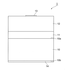
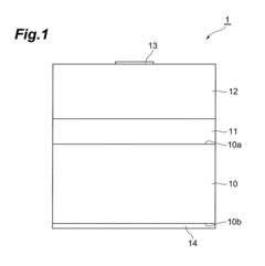
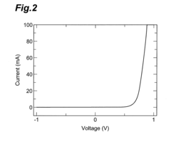
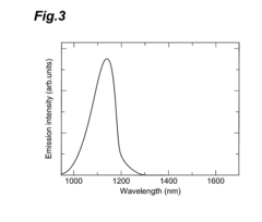
Silicon light-emitting element
PatentInactiveUS20110220956A1
Innovation
- A silicon light-emitting element with a specific structure including a silicon substrate, an insulating film, and a silicon layer with controlled carrier concentrations and film thicknesses, where the insulating film is 0.3 nm to 5 nm thick, allowing efficient light emission with a wavelength easily transmitted through silicon waveguides.
Active manipulation of light in a silicon-on-insulator (SOI) structure
PatentInactiveUS20050189591A1
Innovation
- A silicon-insulator-silicon capacitive (SISCAP) structure with a sub-micron thick SOI layer, a thin dielectric gate oxide layer, and an overlying polysilicon layer, where doped regions are formed to manipulate light by modifying refractive indices with electrical bias, enabling the creation of optical devices like switches, filters, and interferometers using conventional CMOS processing techniques.

Fabrication Processes and Scalability
Silicon photonics fabrication processes have evolved significantly to meet the demands of efficient light manipulation. The primary fabrication method involves photolithography, which uses light to transfer patterns onto silicon wafers. This process begins with the deposition of photoresist onto a silicon-on-insulator (SOI) wafer, followed by exposure to UV light through a mask. The exposed areas are then developed, leaving a pattern that guides subsequent etching steps.
Etching techniques, such as reactive ion etching (RIE) and deep reactive ion etching (DRIE), are crucial for creating precise structures in silicon. These methods allow for the formation of waveguides, resonators, and other photonic components with nanometer-scale precision. The ability to control etch depth and sidewall angles is critical for maintaining optical performance.
Deposition processes, including chemical vapor deposition (CVD) and atomic layer deposition (ALD), are used to add layers of materials such as silicon dioxide for cladding or doping elements to modify the optical properties of silicon. These processes enable the creation of complex multi-layer structures necessary for advanced photonic devices.
Scalability is a key consideration in silicon photonics fabrication. The industry has made significant strides in adapting CMOS (Complementary Metal-Oxide-Semiconductor) fabrication techniques to photonics, allowing for high-volume production. This compatibility with existing semiconductor manufacturing infrastructure is a major advantage, enabling cost-effective scaling of production.
However, challenges remain in achieving consistent quality across large wafers. Variations in film thickness, refractive index, and feature dimensions can significantly impact device performance. Advanced process control and metrology techniques are being developed to address these issues, including in-situ monitoring and feedback systems.
The integration of electronic and photonic components on a single chip presents additional fabrication challenges. Techniques such as wafer bonding and heterogeneous integration are being refined to combine different materials and functionalities while maintaining high yield and reliability.
As the field progresses, new fabrication methods are emerging. These include 3D printing techniques for rapid prototyping of photonic structures and nanoimprint lithography for high-throughput, low-cost production of nanoscale features. These innovations promise to further enhance the scalability and cost-effectiveness of silicon photonics manufacturing.
Integration with Electronic Circuits
The integration of silicon photonics with electronic circuits represents a crucial advancement in the field of efficient light manipulation. This convergence of technologies offers significant potential for enhancing the performance and functionality of optoelectronic systems. By combining the high-speed data processing capabilities of electronic circuits with the efficient light transmission and manipulation of silicon photonics, integrated systems can achieve unprecedented levels of performance and miniaturization.
One of the primary challenges in integrating silicon photonics with electronic circuits lies in the development of efficient interfaces between the optical and electrical domains. Researchers have made substantial progress in this area, developing novel techniques for seamless signal conversion and transmission between photonic and electronic components. These advancements have led to the creation of hybrid optoelectronic circuits that leverage the strengths of both technologies.
The integration process typically involves the co-fabrication of photonic and electronic components on a single chip or the development of sophisticated packaging techniques to combine separately fabricated photonic and electronic elements. Both approaches present unique challenges and opportunities, with ongoing research focused on optimizing manufacturing processes and improving overall system performance.
Recent developments in the field have demonstrated the feasibility of integrating silicon photonic components with CMOS (Complementary Metal-Oxide-Semiconductor) electronics, paving the way for large-scale production of integrated optoelectronic systems. This integration enables the creation of compact, high-performance devices for applications such as data centers, telecommunications, and sensing systems.
The synergy between silicon photonics and electronic circuits has also led to advancements in areas such as on-chip optical interconnects, which offer significant advantages over traditional electrical interconnects in terms of bandwidth, power consumption, and signal integrity. These integrated systems have the potential to revolutionize high-performance computing and communication technologies.
As research in this field continues to progress, we can expect to see further improvements in the integration of silicon photonics with electronic circuits. This includes the development of more efficient interfaces, enhanced manufacturing techniques, and novel architectures that fully exploit the capabilities of both technologies. The ongoing advancements in this area are likely to drive innovation across a wide range of industries, from telecommunications to healthcare, and contribute significantly to the evolution of next-generation optoelectronic systems.
Unlock deeper insights with Patsnap Eureka Quick Research — get a full tech report to explore trends and direct your research. Try now!
Generate Your Research Report Instantly with AI Agent
Supercharge your innovation with Patsnap Eureka AI Agent Platform!