Silicon photonics for precise optical clock distribution.
JUL 17, 20259 MIN READ
Generate Your Research Report Instantly with AI Agent
PatSnap Eureka helps you evaluate technical feasibility & market potential.
Silicon Photonics Background and Objectives
Silicon photonics has emerged as a revolutionary technology in the field of integrated optics, offering the potential to overcome the limitations of traditional electronic systems. The development of silicon photonics can be traced back to the late 1980s, with significant advancements occurring in the past two decades. This technology leverages the well-established silicon manufacturing infrastructure, enabling the integration of optical components with electronic circuits on a single chip.
The evolution of silicon photonics has been driven by the increasing demand for high-speed data transmission and processing in various applications, including telecommunications, data centers, and high-performance computing. As data rates continue to escalate, traditional electronic interconnects face challenges in terms of bandwidth, power consumption, and signal integrity. Silicon photonics offers a promising solution to these issues by utilizing light for data transmission and processing.
In the context of precise optical clock distribution, silicon photonics presents a compelling approach to address the growing need for accurate timing in complex electronic systems. Conventional electrical clock distribution networks face limitations in terms of skew, jitter, and power consumption, particularly as clock frequencies increase and chip sizes expand. Optical clock distribution using silicon photonics has the potential to overcome these challenges by providing low-latency, low-jitter, and low-power clock signal distribution across large chip areas.
The primary objectives of research in silicon photonics for precise optical clock distribution are multifaceted. Firstly, there is a focus on developing high-performance optical modulators and detectors capable of operating at the required clock frequencies with minimal jitter and power consumption. Secondly, researchers aim to design and optimize on-chip optical waveguides and resonators to efficiently distribute clock signals across the chip while maintaining signal integrity. Additionally, there is a strong emphasis on integrating these optical components with existing CMOS electronics to create hybrid electro-optical systems.
Another crucial objective is to enhance the precision and stability of optical clock generation and distribution. This involves developing advanced techniques for on-chip laser integration, wavelength stabilization, and phase-locked loops to ensure accurate and reliable clock signals. Furthermore, researchers are exploring novel architectures for optical clock distribution networks that can scale to accommodate increasingly complex chip designs and multi-chip systems.
As silicon photonics technology continues to mature, the long-term goal is to establish a robust and cost-effective platform for precise optical clock distribution that can be seamlessly integrated into next-generation electronic systems. This includes addressing challenges related to thermal management, packaging, and large-scale manufacturing to enable widespread adoption of silicon photonics-based clock distribution in commercial applications.
Market Demand Analysis for Optical Clock Distribution
The market demand for precise optical clock distribution using silicon photonics technology is experiencing significant growth, driven by the increasing need for high-performance computing and communication systems. As data centers, telecommunications networks, and advanced computing applications continue to evolve, the demand for more efficient and accurate timing solutions becomes paramount.
In the data center market, the push for higher data rates and lower latency is creating a strong demand for precise clock distribution systems. Silicon photonics-based solutions offer the potential to overcome the limitations of traditional electronic clock distribution, providing better timing accuracy and reduced power consumption. This is particularly crucial for synchronizing multiple processors and ensuring data integrity in large-scale computing environments.
The telecommunications sector is another key driver of market demand for optical clock distribution. With the ongoing rollout of 5G networks and the anticipated transition to 6G in the future, there is a growing need for ultra-precise timing in network infrastructure. Silicon photonics-based clock distribution can help meet the stringent synchronization requirements of these advanced wireless networks, enabling improved network performance and reliability.
In the field of high-performance computing and artificial intelligence, the demand for precise clock distribution is also on the rise. As AI models become more complex and distributed computing architectures more prevalent, maintaining accurate timing across multiple processing units becomes critical. Silicon photonics offers a promising solution to address these challenges, potentially unlocking new levels of performance in AI and machine learning applications.
The financial services industry represents another significant market for optical clock distribution technology. High-frequency trading and other time-sensitive financial operations require extremely precise timing to maintain fairness and efficiency in transactions. Silicon photonics-based clock distribution systems can provide the necessary timing accuracy to support these demanding applications.
Emerging technologies such as quantum computing and advanced sensing systems also contribute to the growing market demand for precise optical clock distribution. These cutting-edge fields often require unprecedented levels of timing accuracy, which silicon photonics is well-positioned to deliver.
The global market for silicon photonics, including applications in clock distribution, is projected to grow substantially in the coming years. While specific market size figures for optical clock distribution are not readily available, the overall silicon photonics market is expected to expand significantly, driven in part by the demand for precise timing solutions.
As industries continue to push the boundaries of performance and efficiency, the market for silicon photonics-based optical clock distribution is likely to see sustained growth. The technology's potential to address critical timing challenges across various sectors positions it as a key enabler for next-generation computing and communication systems.
Current Challenges in Silicon Photonics Clock Distribution
Silicon photonics has emerged as a promising technology for precise optical clock distribution, offering potential advantages in terms of speed, power efficiency, and integration. However, several significant challenges currently hinder the widespread adoption and implementation of this technology in practical applications.
One of the primary challenges is the precise control and management of optical signal propagation within silicon-based waveguides. Silicon's high refractive index leads to strong light confinement, which can result in increased propagation losses and unwanted mode coupling. This issue becomes particularly critical in clock distribution networks, where maintaining signal integrity and minimizing jitter are paramount.
Thermal management presents another substantial hurdle in silicon photonics clock distribution systems. Silicon's thermo-optic coefficient causes significant changes in refractive index with temperature fluctuations, leading to phase shifts and timing errors in the distributed clock signals. Developing effective thermal compensation techniques and stable temperature control mechanisms is crucial for ensuring reliable and accurate clock distribution.
The integration of optical components with electronic circuits poses a considerable challenge. While silicon photonics offers the potential for seamless integration with CMOS technology, achieving low-loss, high-bandwidth interfaces between optical and electrical domains remains difficult. This integration challenge extends to the development of efficient electro-optic modulators and photodetectors that can operate at the high speeds required for precise clock distribution.
Polarization management is another critical issue in silicon photonics clock distribution systems. The high birefringence of silicon waveguides can lead to polarization-dependent losses and dispersion, potentially causing signal distortion and timing errors. Developing polarization-insensitive components and effective polarization control techniques is essential for robust clock distribution networks.
Fabrication tolerances and variability present ongoing challenges in silicon photonics. The performance of optical components is highly sensitive to dimensional variations, which can significantly impact the phase and amplitude of propagating signals. Achieving consistent and reproducible device characteristics across large-scale integrated circuits is crucial for reliable clock distribution.
Lastly, the development of efficient and scalable clock distribution network architectures remains a significant challenge. Designing optimal topologies that can deliver precise timing signals to multiple points across a chip while minimizing power consumption and maintaining signal integrity is a complex task. This challenge is further compounded by the need to account for variations in optical path lengths and potential crosstalk between adjacent waveguides.
Addressing these challenges requires interdisciplinary research efforts, combining expertise in photonics, electronics, materials science, and system design. Overcoming these hurdles will be crucial for realizing the full potential of silicon photonics in precise optical clock distribution and enabling its widespread adoption in next-generation integrated circuits and high-performance computing systems.
Existing Silicon Photonics Clock Distribution Solutions
01 Precision manufacturing of silicon photonic devices
Advanced manufacturing techniques are employed to create high-precision silicon photonic devices. These methods ensure accurate fabrication of nanoscale structures, waveguides, and other components essential for optimal performance in silicon photonics applications. Precision manufacturing enables better control over optical properties and device functionality.- Precision manufacturing of silicon photonic devices: Advanced manufacturing techniques are employed to create high-precision silicon photonic devices. These methods ensure accurate fabrication of nanoscale structures, waveguides, and other components essential for optimal performance in silicon photonics applications. Precision manufacturing enables the production of devices with minimal defects and tight tolerances, crucial for maintaining signal integrity and reducing optical losses.
- Integration of silicon photonics with electronic circuits: Silicon photonics technology is integrated with electronic circuits to create hybrid optoelectronic systems. This integration allows for efficient conversion between optical and electrical signals, enabling high-speed data transmission and processing. The combination of photonic and electronic components on a single chip enhances overall system performance and reduces power consumption in various applications, including telecommunications and data centers.
- Precision alignment and packaging of silicon photonic devices: Specialized techniques are developed for precise alignment and packaging of silicon photonic devices. These methods ensure accurate positioning of optical components, fibers, and other elements relative to the silicon chip. Precision alignment is critical for minimizing coupling losses and maintaining signal quality in complex photonic systems. Advanced packaging solutions protect the delicate photonic structures while facilitating integration with other system components.
- Precision control of optical properties in silicon photonics: Methods are developed to precisely control the optical properties of silicon photonic devices. These techniques involve manipulating material characteristics, geometry, and environmental factors to achieve desired optical behaviors. Precision control enables the creation of tunable devices, filters, and modulators with high performance and reliability. This capability is essential for applications requiring dynamic adjustment of optical properties, such as reconfigurable optical networks.
- High-precision measurement and characterization of silicon photonic devices: Advanced measurement and characterization techniques are developed for silicon photonic devices. These methods enable accurate assessment of device performance, including parameters such as insertion loss, crosstalk, and spectral response. High-precision measurement is crucial for quality control, device optimization, and system-level integration. Characterization tools and methodologies support the development of increasingly complex and high-performance silicon photonic systems.
02 Integration of silicon photonics with electronic circuits
Silicon photonics technology is integrated with electronic circuits to create hybrid optoelectronic systems. This integration allows for improved data transmission speeds, reduced power consumption, and enhanced overall performance in various applications such as telecommunications and data centers.Expand Specific Solutions03 Precision alignment and packaging of silicon photonic components
Techniques for precise alignment and packaging of silicon photonic components are developed to ensure optimal performance and reliability. These methods address challenges in coupling light between different components and interfacing silicon photonic devices with external optical fibers or other systems.Expand Specific Solutions04 Advanced materials for silicon photonics
Novel materials and material combinations are explored to enhance the performance of silicon photonic devices. These materials may offer improved optical properties, better compatibility with existing manufacturing processes, or enable new functionalities in silicon photonics applications.Expand Specific Solutions05 Precision measurement and characterization of silicon photonic devices
Advanced measurement and characterization techniques are developed to assess the performance and quality of silicon photonic devices with high precision. These methods enable accurate evaluation of optical properties, device functionality, and manufacturing tolerances, contributing to the improvement of silicon photonics technology.Expand Specific Solutions
Key Players in Silicon Photonics Industry
The research on silicon photonics for precise optical clock distribution is in a rapidly evolving phase, with significant market potential and technological advancements. The industry is transitioning from early-stage development to more mature applications, driven by the increasing demand for high-speed data transmission and low-latency communication. Major players like IBM, Toshiba, and TSMC are investing heavily in this technology, leveraging their expertise in semiconductor manufacturing. Academic institutions such as Caltech and EPFL are contributing cutting-edge research, while specialized companies like Lumentum are focusing on commercialization. The market is expected to grow substantially as silicon photonics becomes integral to next-generation computing and communication systems, with a diverse ecosystem of companies and research institutions collaborating to overcome technical challenges and push the boundaries of this promising field.
International Business Machines Corp.
Technical Solution: IBM has developed advanced silicon photonics technology for precise optical clock distribution. Their approach integrates nanophotonic waveguides directly on CMOS chips, enabling on-chip optical interconnects. The company has demonstrated a silicon photonic transceiver operating at 56 Gb/s per wavelength[1], with potential for multi-wavelength operation to achieve Tb/s data rates. IBM's technology utilizes wavelength division multiplexing (WDM) to distribute multiple clock signals simultaneously, enhancing synchronization across large chip areas. They have also implemented electro-optic modulators and photodetectors in silicon, allowing for efficient conversion between electrical and optical domains[2].
Strengths: High integration with CMOS, scalability to high data rates, and potential for multi-core synchronization. Weaknesses: Complexity in manufacturing and potential thermal management issues in dense photonic-electronic integration.
Taiwan Semiconductor Manufacturing Co., Ltd.
Technical Solution: TSMC has made significant strides in silicon photonics for precise optical clock distribution. Their approach focuses on integrating photonic components with advanced CMOS nodes, leveraging their expertise in semiconductor manufacturing. TSMC has developed a platform that includes low-loss silicon waveguides, high-speed modulators, and sensitive photodetectors. They have demonstrated optical links operating at speeds up to 112 Gb/s per wavelength[3], with a roadmap to higher data rates. TSMC's technology also incorporates on-chip laser integration, crucial for compact and energy-efficient optical clock distribution systems. Their process allows for the co-integration of photonics with high-performance logic, enabling tightly coupled optoelectronic systems[4].
Strengths: Advanced manufacturing capabilities, high integration density, and compatibility with leading-edge CMOS nodes. Weaknesses: Potential yield challenges in combined photonic-electronic processes and higher initial costs compared to pure electronic solutions.
Core Innovations in Optical Clock Distribution
Designing photonic switching systems utilizing equalized drivers
PatentWO2014039492A1
Innovation
- A system-wide optimization approach that designs photonic switch diodes in conjunction with selecting custom electronic switch driver circuits, employing feed-forward equalization techniques and complimentary metal oxide-semiconductor drivers, to increase the speed of photonic switch diodes without compromising other performance metrics.


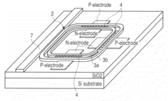
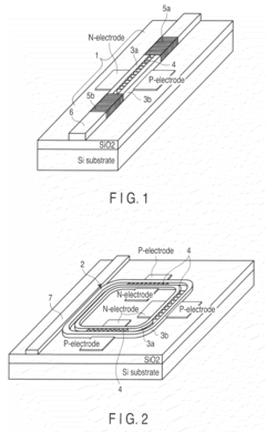
Light-emitting device and manufacturing method of the same
PatentInactiveUS20090245314A1
Innovation
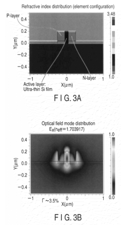
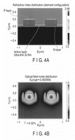
- A semiconductor light-emitting device with a novel structure featuring parallel or ring-shaped semiconductor wires and ultra-thin films interposed between them, with resonator mirrors and p- and n-electrodes, enhancing the light confinement coefficient (Γ) through the 'slot-type waveguide effects', allowing for increased photon energy confinement and efficient laser oscillation.
Integration Challenges and Opportunities
The integration of silicon photonics for precise optical clock distribution presents both significant challenges and exciting opportunities. One of the primary challenges lies in the precise alignment and coupling of optical components within the silicon photonic integrated circuits (PICs). The nanometer-scale precision required for efficient light transmission between waveguides, modulators, and detectors demands advanced fabrication techniques and innovative design strategies.
Thermal management is another critical challenge in silicon photonic integration. The thermo-optic effect in silicon can cause wavelength shifts and performance degradation, necessitating careful temperature control and compensation mechanisms. This challenge is particularly acute in high-performance computing applications where clock distribution accuracy is paramount.
Despite these challenges, the integration of silicon photonics offers tremendous opportunities for improving clock distribution in large-scale systems. The ability to transmit optical signals with low latency and minimal skew across long distances on-chip and between chips can significantly enhance system synchronization and performance. This is especially valuable in data centers and high-performance computing environments where precise timing is crucial.
The scalability of silicon photonics manufacturing processes aligns well with existing CMOS fabrication techniques, offering a path to cost-effective, large-scale production of integrated optical clock distribution networks. This compatibility with established semiconductor manufacturing infrastructure presents an opportunity for rapid adoption and integration into existing electronic systems.
Furthermore, the integration of silicon photonics enables the development of novel architectures for clock distribution. For instance, the implementation of optical frequency combs on-chip could provide multiple, precisely spaced clock signals from a single source, offering new possibilities for multi-clock domain designs and frequency synthesis.
The ongoing development of advanced materials and structures, such as III-V on silicon integration and silicon-germanium alloys, opens up new avenues for enhancing the performance of integrated photonic clock distribution systems. These advancements could lead to improved light generation, modulation, and detection capabilities within the silicon photonic platform.
Energy Efficiency and Thermal Management
Energy efficiency and thermal management are critical considerations in the development of silicon photonics for precise optical clock distribution. As these systems become more complex and integrated, power consumption and heat dissipation emerge as significant challenges that must be addressed to ensure optimal performance and reliability.
Silicon photonics offers inherent advantages in energy efficiency compared to traditional electronic systems. The use of light for signal transmission reduces power consumption associated with electrical resistance and capacitance. However, as clock distribution networks scale up to meet the demands of larger and more complex systems, energy efficiency becomes increasingly important.
One key area of focus is the optimization of optical modulators and detectors, which are essential components in clock distribution networks. Research efforts are directed towards developing low-power modulators that can operate at high speeds while minimizing energy consumption. Similarly, high-sensitivity detectors are being designed to reduce the optical power required for reliable signal detection, further improving overall system efficiency.
Thermal management is closely linked to energy efficiency in silicon photonic systems. As power consumption increases, so does heat generation, which can adversely affect the performance and reliability of photonic components. Temperature fluctuations can lead to wavelength shifts in optical devices, potentially causing signal degradation or system failures.
To address these thermal challenges, researchers are exploring various approaches. One strategy involves the integration of thermal sensors and active cooling systems directly on the silicon photonic chip. These systems can monitor temperature variations in real-time and adjust cooling mechanisms accordingly, maintaining optimal operating conditions for photonic components.
Another area of investigation is the development of novel materials and structures that enhance heat dissipation. For example, the use of thermally conductive materials in chip packaging and the implementation of advanced heat sink designs can significantly improve thermal management in silicon photonic systems.
Furthermore, researchers are exploring the potential of heterogeneous integration, combining silicon photonics with other materials that offer superior thermal properties. This approach could lead to hybrid systems that leverage the strengths of different materials to achieve both high performance and effective thermal management.
Unlock deeper insights with PatSnap Eureka Quick Research — get a full tech report to explore trends and direct your research. Try now!
Generate Your Research Report Instantly with AI Agent
Supercharge your innovation with PatSnap Eureka AI Agent Platform!