SEM-EDS Low-kV Microanalysis: Surface Sensitivity, L Lines And Limits Of Detection
SEP 22, 20259 MIN READ
Generate Your Research Report Instantly with AI Agent
Patsnap Eureka helps you evaluate technical feasibility & market potential.
SEM-EDS Low-kV Microanalysis Background and Objectives
Scanning Electron Microscopy with Energy Dispersive X-ray Spectroscopy (SEM-EDS) has evolved significantly since its inception in the 1960s. The technique combines the high-resolution imaging capabilities of SEM with the elemental analysis power of EDS, making it an indispensable tool in materials science, geology, forensics, and semiconductor industries. Traditional SEM-EDS analysis typically operates at accelerating voltages of 15-20 kV, which provides good excitation for K-lines of elements across a wide atomic number range.
The emergence of low-kV microanalysis (typically below 5 kV) represents a significant technological shift in the field. This approach has gained prominence over the past decade as researchers and industries increasingly demand higher spatial resolution and enhanced surface sensitivity for nanomaterials, thin films, and delicate specimens that cannot withstand high electron beam energies.
The evolution of low-kV microanalysis has been driven by advancements in detector technology, particularly the development of silicon drift detectors (SDDs) with improved energy resolution and sensitivity at low energies. Parallel improvements in electron optics and source brightness have enabled the maintenance of adequate probe currents at lower accelerating voltages, facilitating practical analysis at these conditions.
A key technological trend in this field is the increasing focus on L-line analysis for heavier elements rather than traditional K-lines, as L-lines can be efficiently excited at lower accelerating voltages. This shift necessitates new approaches to quantification algorithms and standards, as L-lines present unique challenges including peak overlaps and absorption effects that differ from K-line analysis.
The primary objectives of advancing low-kV SEM-EDS microanalysis are multifaceted. First, to enhance surface sensitivity for analyzing the uppermost layers of materials (typically <1 μm), which is critical for thin films, coatings, and surface treatments. Second, to improve spatial resolution by reducing the interaction volume of the electron beam with the sample, enabling more precise analysis of nanoscale features and interfaces.
Additional goals include minimizing beam damage to electron-sensitive materials such as polymers, biological specimens, and certain semiconductors, while simultaneously pushing the limits of detection to lower concentrations despite the reduced X-ray yield at low accelerating voltages. The field also aims to develop more sophisticated quantification methods specifically optimized for L-line analysis, addressing challenges like peak overlaps and absorption effects.
The ultimate technological objective is to establish reliable, standardized methodologies for low-kV microanalysis that can be widely adopted across industries, ensuring consistent and comparable results regardless of the specific instrumentation used, while maintaining the analytical power traditionally associated with higher-kV operations.
Market Applications and Demand Analysis for Low-kV Microanalysis
The market for Low-kV Microanalysis technologies has experienced significant growth over the past decade, driven by increasing demands for advanced materials characterization in various industries. The global analytical instrumentation market, which includes SEM-EDS systems, was valued at approximately $30 billion in 2022, with the electron microscopy segment showing consistent annual growth rates of 6-8%.
Surface-sensitive analysis capabilities offered by Low-kV SEM-EDS have become particularly valuable in semiconductor manufacturing, where the continuous miniaturization of components requires precise characterization of thin films and interfaces. The semiconductor industry's demand for these technologies has been bolstered by the global chip shortage and subsequent investments in manufacturing capacity, creating a robust market for advanced analytical tools.
Materials science research represents another significant market segment, with universities and research institutions investing in Low-kV microanalysis capabilities to study nanomaterials, composites, and advanced alloys. The ability to analyze L-lines at low accelerating voltages has opened new possibilities for characterizing light elements in complex matrices, addressing a long-standing limitation in traditional EDS analysis.
The pharmaceutical and life sciences sectors have also emerged as growing markets for Low-kV microanalysis. These industries require non-destructive surface analysis of biological samples and drug delivery systems, where conventional high-voltage techniques might damage sensitive specimens or provide insufficient surface detail.
Environmental monitoring and forensic science applications have created additional demand, particularly for portable or field-deployable systems that can provide rapid elemental analysis with minimal sample preparation. The improved detection limits of modern Low-kV systems make them suitable for trace element analysis in environmental samples and evidence materials.
Geographically, North America and Europe currently dominate the market for advanced microanalysis technologies, accounting for approximately 60% of global demand. However, the Asia-Pacific region, particularly China, South Korea, and Taiwan, shows the fastest growth rate, driven by expanding semiconductor manufacturing capabilities and increasing research investments.
Market forecasts suggest that the demand for Low-kV microanalysis will continue to grow at a compound annual rate of 7-9% through 2028, outpacing the broader analytical instrumentation market. This growth will be fueled by ongoing technological advancements that improve detection limits and spatial resolution, as well as software developments that enhance data interpretation and automation capabilities.
Current Challenges in Surface Sensitivity and Detection Limits
Despite significant advancements in SEM-EDS microanalysis technology, several critical challenges persist in achieving optimal surface sensitivity and detection limits when operating at low accelerating voltages. The fundamental physics of electron beam interactions creates inherent limitations that researchers and instrument manufacturers continue to grapple with. Primary among these is the signal-to-noise ratio degradation that occurs at low-kV settings, where reduced beam energy generates fewer characteristic X-rays while background contributions remain proportionally higher.
The accurate quantification of light elements (Z<11) presents another significant hurdle, as their low-energy X-rays are highly susceptible to absorption within the sample itself. This self-absorption effect becomes particularly problematic when analyzing complex matrices or layered structures, where compositional gradients can dramatically alter X-ray generation and detection efficiency. Additionally, the overlap between L-lines of heavier elements and K-lines of lighter elements creates spectral interference that conventional deconvolution algorithms struggle to resolve completely.
Surface contamination emerges as a persistent challenge in low-kV microanalysis, where even nanometer-scale carbon deposits from electron beam interaction with residual hydrocarbons can significantly alter analytical results. This contamination layer attenuates both incoming electrons and outgoing X-rays, introducing systematic errors that are difficult to quantify and correct, especially for samples with irregular topography.
The physical limitations of EDS detector technology further constrain detection capabilities. While silicon drift detectors (SDDs) have substantially improved energy resolution compared to earlier Si(Li) detectors, they still typically achieve only 120-130 eV resolution at Mn Kα (5.9 keV), which proves insufficient for complete separation of closely spaced peaks in complex spectra. This resolution limitation becomes particularly problematic when analyzing trace elements in the presence of major constituents with overlapping spectral lines.
Standardless quantification algorithms, while convenient, introduce additional uncertainties in low-kV analysis. These algorithms rely on theoretical models and assumptions about sample composition that may not accurately represent the complex near-surface region being analyzed. The fundamental parameter approach, though sophisticated, struggles with heterogeneous samples where the assumption of homogeneity breaks down at the micro and nanoscale.
Beam damage represents another significant challenge, particularly for beam-sensitive materials like polymers, biological specimens, and certain semiconductors. The electron dose required for adequate X-ray statistics often exceeds the damage threshold of these materials, creating a fundamental trade-off between analytical precision and sample preservation that limits practical applications.
Existing Methodologies for L-Line Analysis and Surface Detection
01 Low-kV SEM-EDS for enhanced surface sensitivity
Low-kV scanning electron microscopy with energy dispersive spectroscopy (SEM-EDS) provides enhanced surface sensitivity by reducing the electron beam penetration depth. This technique allows for more accurate analysis of thin films, coatings, and surface features by limiting the interaction volume to the near-surface region. The reduced accelerating voltage enables better detection of light elements and improves spatial resolution for surface characterization, making it particularly valuable for nanomaterial analysis and semiconductor inspection.- Low-kV SEM-EDS for enhanced surface sensitivity: Low-kV scanning electron microscopy with energy dispersive spectroscopy (SEM-EDS) provides enhanced surface sensitivity by reducing the electron beam penetration depth. This technique allows for more accurate analysis of thin films, coatings, and surface features by limiting the interaction volume to the near-surface region. The reduced accelerating voltage enables better detection of light elements and improves spatial resolution for surface characterization, making it particularly valuable for nanomaterial analysis and semiconductor inspection.
- L-line analysis for improved elemental detection: L-line analysis in SEM-EDS offers advantages for detecting and quantifying certain elements, particularly heavy metals, when operating at low accelerating voltages. By utilizing L-series X-ray emissions instead of K-lines, analysts can achieve better signal-to-noise ratios and improved quantification at lower beam energies. This approach enables more accurate compositional analysis of surface layers while minimizing beam damage to sensitive samples. The technique is particularly valuable for distinguishing elements with overlapping K-lines or when analyzing materials containing high atomic number elements.
- Detection limits optimization in low-kV microanalysis: Optimizing detection limits in low-kV SEM-EDS microanalysis involves several strategies including longer acquisition times, optimized detector positioning, and advanced signal processing algorithms. Modern EDS systems incorporate improved detector technologies with higher sensitivity and better energy resolution to enhance detection of trace elements at low accelerating voltages. Specialized calibration procedures and matrix correction methods are employed to account for the unique challenges of quantification at low-kV, enabling detection of elements at concentrations below traditional limits while maintaining accuracy.
- Advanced detector technologies for surface microanalysis: Advanced detector technologies have significantly improved SEM-EDS capabilities for surface microanalysis. Silicon drift detectors (SDDs) with improved collection efficiency and energy resolution enable better element discrimination at low accelerating voltages. Windowless or ultra-thin window detectors enhance light element detection capabilities. Some systems incorporate multiple detectors at optimized geometries to maximize X-ray collection while minimizing shadowing effects. These technological advancements allow for faster acquisition times and improved spatial resolution in surface-sensitive applications.
- Quantitative analysis methods for low-kV SEM-EDS: Specialized quantitative analysis methods have been developed to address the challenges of low-kV SEM-EDS microanalysis. These include modified matrix correction algorithms that account for the unique X-ray generation and absorption characteristics at low accelerating voltages. Monte Carlo simulations are employed to model electron beam interactions and improve quantification accuracy. Standards-based and standardless analysis approaches have been adapted specifically for low-kV conditions, incorporating corrections for surface roughness, thin film effects, and charging phenomena to achieve reliable compositional data from surface-sensitive measurements.
02 L-line X-ray analysis for improved elemental detection
L-line X-ray analysis in SEM-EDS offers advantages for detecting certain elements, particularly heavy metals, when operating at low accelerating voltages. Using L-lines instead of K-lines allows for efficient X-ray generation at lower beam energies, improving surface sensitivity while maintaining analytical capabilities. This approach provides better peak separation for adjacent elements in the periodic table and can enhance quantitative analysis accuracy when proper standards and correction factors are applied.Expand Specific Solutions03 Detection limits and quantification in low-kV microanalysis
The limits of detection in low-kV SEM-EDS microanalysis are influenced by several factors including beam current, acquisition time, detector efficiency, and sample composition. While low-kV operation improves spatial resolution and surface sensitivity, it can reduce overall X-ray yield and statistical precision. Advanced detector technologies with improved collection efficiency and signal-to-noise ratios help overcome these limitations. Quantitative analysis at low-kV requires specialized standards and correction algorithms to account for the unique X-ray generation and absorption characteristics at reduced accelerating voltages.Expand Specific Solutions04 Advanced detector technologies for low-kV microanalysis
Modern SEM-EDS systems incorporate advanced detector technologies specifically designed for low-kV microanalysis. Silicon drift detectors (SDDs) with improved energy resolution and higher count rates enable better element discrimination and faster data acquisition. Windowless or ultra-thin window detectors enhance light element detection capabilities. Some systems feature multiple detectors positioned at different angles to maximize X-ray collection efficiency and provide complementary information about surface topography and composition, significantly improving the sensitivity and reliability of low-kV microanalysis.Expand Specific Solutions05 Sample preparation and analytical protocols for optimal results
Proper sample preparation and analytical protocols are crucial for achieving optimal results in low-kV SEM-EDS microanalysis. Surface cleaning techniques to remove contamination, conductive coatings to prevent charging, and flat polishing to minimize topographic effects all contribute to improved data quality. Standardized protocols for beam current selection, working distance optimization, and detector positioning help maximize signal collection while minimizing artifacts. Calibration using appropriate standards that match the analysis conditions ensures accurate quantification, particularly when working with L-lines and near-surface analysis.Expand Specific Solutions
Leading Manufacturers and Research Institutions in Microanalysis
SEM-EDS Low-kV Microanalysis is currently in a growth phase, with increasing adoption across materials science, semiconductor, and nanotechnology sectors. The market size is expanding steadily, driven by demand for high-resolution surface analysis capabilities in R&D and quality control applications. Technologically, this field is reaching maturity with key players like Hitachi High-Tech, Oxford Instruments, and FEI Co. leading innovation in low-voltage electron microscopy systems. Applied Materials and ASML are leveraging this technology for semiconductor process control, while research institutions like Max Planck Society and Industrial Technology Research Institute are advancing fundamental capabilities. EDAX and Gatan have specialized in developing enhanced EDS detectors optimized for low-kV applications, improving surface sensitivity and detection limits that are critical for nanoscale material characterization.
Hitachi High-Tech America, Inc.
Technical Solution: Hitachi High-Tech America's SEM-EDS low-kV microanalysis solution builds on Hitachi's core technologies with adaptations for the American market. Their systems feature high-brightness field emission sources coupled with specialized optics that maintain probe current and spatial resolution even at accelerating voltages below 5kV. Their EDS detectors employ advanced silicon drift technology with optimized geometry and ultra-thin windows to maximize collection efficiency for low-energy X-rays. Hitachi High-Tech's approach emphasizes system integration, with hardware and software components designed to work together seamlessly for optimal low-kV performance. Their analysis software includes specialized routines for L-line quantification, with comprehensive reference data and models that account for the complex physics of X-ray generation and detection at low accelerating voltages. The systems incorporate automated procedures for optimizing working distance, beam current, and detector positioning to maximize analytical sensitivity while minimizing beam damage. Hitachi High-Tech has developed specific applications targeting semiconductor, materials science, and biological samples where surface sensitivity and minimal beam damage are critical requirements.
Strengths: Excellent system integration with optimized hardware and software components; superior beam stability at low-kV; comprehensive application support for diverse industries. Weaknesses: Premium pricing compared to more basic systems; requires regular maintenance to maintain optimal performance; learning curve for advanced features can be steep.
Oxford Instruments NanoTechnology Tools Ltd.
Technical Solution: Oxford Instruments has developed the X-Max Extreme SEM-EDS system specifically designed for low-kV microanalysis applications. This system features an innovative large-area silicon drift detector (SDD) with specialized window technology that maximizes transmission of low-energy X-rays. Their approach combines hardware optimization with advanced software algorithms to address the challenges of low-kV analysis. The system employs proprietary pulse processing technology that improves count rates while maintaining energy resolution at low accelerating voltages. Oxford's TruMap deconvolution algorithms specifically address peak overlaps in L-line spectra, which are critical for accurate analysis at low-kV. Their Aztec software platform includes specialized routines for surface sensitivity analysis and thin-film applications, with capabilities to model depth-dependent X-ray generation and absorption effects. The system also incorporates advanced standardless quantification methods calibrated specifically for low-kV operation, with specialized reference data for L-line analysis of transition metals and heavier elements.
Strengths: Industry-leading detector technology with exceptional low-energy efficiency; comprehensive software suite specifically optimized for low-kV applications; excellent integration with various SEM platforms. Weaknesses: Premium pricing may be prohibitive for some users; complex software features require significant training; quantification accuracy remains challenging for heterogeneous samples.
Key Innovations in Low-kV Detection and Signal Processing
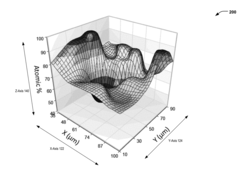
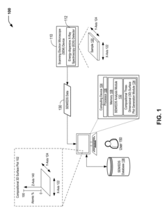
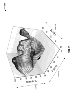
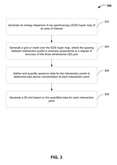
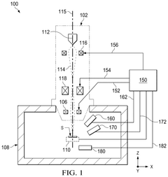
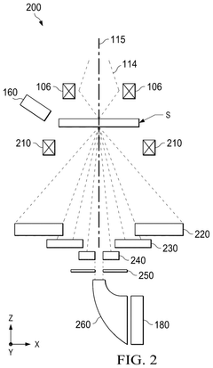
Compositional three-dimensional surface plots
PatentInactiveUS20170329936A1
Innovation
- A method and system that utilize SEM/EDS data to generate compositional three-dimensional surface plots, where the Z-axis represents atomic or weight percentage composition, enabling quantitative data visualization for each location of a sample, by receiving and processing data from a scanning electron microscope equipped with an EDS detector.
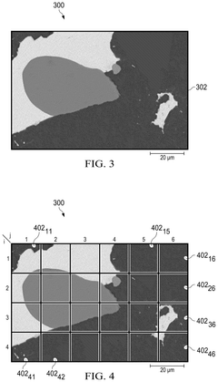
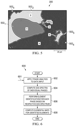
Elemental identification based on phase analysis
PatentPendingUS20250231127A1
Innovation
- Implementing phase analysis and multivariate statistical analysis to compute phase maps and elemental maps by binning pixelwise energy-dispersive X-ray spectroscopy spectra, allowing for live updates during data acquisition.
Standardization and Calibration Protocols for Low-kV Analysis
Standardization and calibration protocols are critical components for ensuring reliable and reproducible results in low-kV SEM-EDS microanalysis. The reduced accelerating voltage environment presents unique challenges that require specialized calibration approaches distinct from traditional high-voltage methodologies.
The foundation of effective low-kV analysis begins with instrument-specific calibration procedures. These must account for the increased influence of surface contamination, charging effects, and beam instability that become more pronounced at lower accelerating voltages. Calibration standards must be carefully selected to match the analytical conditions, with particular attention to standards that provide reliable L-line emissions in the energy range of interest.
Reference materials for low-kV calibration require specific characteristics including high purity, homogeneity at the nanoscale, and stability under electron beam exposure. Pure element standards, while useful for conventional analysis, often prove inadequate for low-kV work due to surface oxidation issues. Instead, stable compounds with well-characterized stoichiometry, such as carefully prepared oxides, silicates, and synthetic minerals, have demonstrated superior performance as calibration references.
Energy calibration protocols must be adapted specifically for the low-kV regime, with particular attention to peak shifts and resolution changes that occur at reduced accelerating voltages. The calibration procedure should include verification steps at multiple points across the energy spectrum, with special focus on the lower energy region where L-lines predominate and resolution challenges are most acute.
Quantification algorithms require significant modification for low-kV analysis. Traditional ZAF and φ(ρz) correction methods must be recalibrated to account for the altered interaction volume and increased significance of surface effects. This necessitates the development of specialized correction factors that accurately model electron scattering and X-ray generation processes under low-kV conditions.
Interlaboratory comparison studies have demonstrated that standardized protocols can significantly improve the consistency of low-kV analytical results across different instruments and operators. These protocols typically include detailed procedures for sample preparation, instrument setup, calibration verification, and data processing that are specifically optimized for low-kV work.
Quality assurance measures for low-kV analysis should include regular verification using secondary standards, drift monitoring, and systematic documentation of calibration parameters. The establishment of uncertainty budgets that account for the unique error sources in low-kV analysis is essential for meaningful interpretation of analytical results.
Environmental and Sample Preparation Factors in Microanalysis
Environmental factors and sample preparation techniques significantly impact the quality and reliability of SEM-EDS low-kV microanalysis. The vacuum environment within the SEM chamber must be carefully controlled to minimize contamination that can interfere with X-ray detection, particularly when working with low energy L-lines that are characteristic of low-kV analysis.
Sample cleanliness is paramount, as surface contaminants can dramatically alter analytical results. Even trace amounts of carbon, oxygen, or other light elements can create misleading spectral peaks or obscure genuine signals. This becomes especially critical when analyzing nanoscale features or thin films where surface sensitivity is heightened at low accelerating voltages.
Specimen preparation protocols must be tailored specifically for low-kV analysis. Traditional preparation methods often introduce artifacts that may be negligible at higher voltages but become significant interference factors at low-kV. Carbon coating, commonly used to enhance conductivity, must be applied with precise thickness control to avoid compromising the detection of light elements while still preventing charging effects.
The geometry of sample mounting affects the take-off angle for X-ray detection, which directly influences the detection efficiency of low-energy L-lines. Optimizing this geometry becomes crucial when working near detection limits, as improper positioning can result in signal attenuation and reduced analytical sensitivity.
Environmental monitoring systems within modern SEM instruments provide real-time feedback on chamber conditions, allowing operators to maintain optimal analytical parameters. Fluctuations in vacuum quality, temperature, or electromagnetic interference can all degrade spectral resolution and compromise detection limits.
Sample homogeneity presents another challenge, as surface roughness creates variable interaction volumes that complicate quantitative analysis. Polishing techniques must balance the need for a flat analytical surface against the risk of introducing preparation artifacts or altering the sample's chemical composition.
For beam-sensitive materials, special considerations include reduced beam current, shorter acquisition times, and cryogenic preparation techniques. These approaches help preserve sample integrity while still enabling the collection of meaningful analytical data at low accelerating voltages.
Standardization procedures for low-kV microanalysis require carefully prepared reference materials that match the matrix composition of the specimens under investigation. This matrix-matching becomes increasingly important as the accelerating voltage decreases and surface effects become more pronounced.
Unlock deeper insights with Patsnap Eureka Quick Research — get a full tech report to explore trends and direct your research. Try now!
Generate Your Research Report Instantly with AI Agent
Supercharge your innovation with Patsnap Eureka AI Agent Platform!