SEM-EDS Spectral Overlaps: Peak Deconvolution, WDS Cross-Checks And Artifacts
SEP 22, 20259 MIN READ
Generate Your Research Report Instantly with AI Agent
Patsnap Eureka helps you evaluate technical feasibility & market potential.
SEM-EDS Technology Evolution and Objectives
Scanning Electron Microscopy with Energy Dispersive X-ray Spectroscopy (SEM-EDS) has evolved significantly since its inception in the 1960s. The technology initially emerged as a revolutionary tool for elemental analysis, combining the imaging capabilities of electron microscopy with the chemical analysis power of X-ray spectroscopy. Early systems were limited by poor energy resolution, low detection efficiency, and rudimentary data processing capabilities, making spectral overlap issues particularly problematic.
The 1980s marked a significant advancement with the introduction of silicon drift detectors (SDDs), which dramatically improved energy resolution and count rates. This technological leap enabled better differentiation between closely spaced spectral peaks, though complete resolution of overlapping peaks remained challenging. The 1990s saw further refinements in detector technology and the integration of digital signal processing, enhancing the system's ability to handle complex spectra.
By the early 2000s, SEM-EDS systems began incorporating sophisticated software algorithms for peak deconvolution, allowing analysts to mathematically separate overlapping spectral peaks with greater accuracy. These developments coincided with improvements in detector sensitivity and stability, reducing artifacts and false readings that had previously plagued the technology.
The past decade has witnessed remarkable progress in both hardware and software components of SEM-EDS systems. Modern detectors now offer energy resolutions approaching 120 eV or better at Mn Kα, significantly reducing but not eliminating spectral overlap issues. Complementary techniques such as Wavelength Dispersive Spectroscopy (WDS) have been increasingly integrated with EDS systems to provide cross-validation capabilities for ambiguous spectral interpretations.
Current technological objectives focus on addressing the persistent challenge of spectral overlaps through multiple approaches. These include developing more sophisticated peak deconvolution algorithms that incorporate machine learning techniques to better distinguish between overlapping peaks based on subtle spectral features. Another objective is the seamless integration of EDS with WDS and other complementary techniques to create comprehensive analytical systems that can automatically identify and resolve spectral ambiguities.
Looking forward, the field aims to achieve near-perfect spectral resolution through continued improvements in detector technology and signal processing. Research is also directed toward developing standardized protocols for identifying and managing artifacts that can lead to misinterpretation of spectral data. The ultimate goal is to create intelligent analytical systems capable of autonomous spectral interpretation with minimal human intervention, particularly in cases of complex overlaps and artifacts that currently require expert analysis.
Market Applications and Demand Analysis
The market for SEM-EDS (Scanning Electron Microscopy with Energy Dispersive X-ray Spectroscopy) technology continues to expand across multiple industries, driven by increasing demands for accurate material characterization and quality control. The global electron microscopy market, which includes SEM-EDS systems, was valued at approximately $4.1 billion in 2022 and is projected to grow at a CAGR of 8% through 2030, with SEM-EDS solutions representing a significant segment of this market.
Materials science and engineering sectors constitute the largest application area, accounting for roughly 35% of the SEM-EDS market. These industries require precise elemental analysis for developing advanced materials, where the ability to resolve spectral overlaps directly impacts product development timelines and material performance characteristics. The semiconductor industry follows closely, representing about 28% of market demand, where nanoscale analysis necessitates extremely accurate elemental identification free from spectral artifacts.
Pharmaceutical and life sciences applications have emerged as the fastest-growing segment, with a growth rate exceeding 10% annually. In these fields, the analysis of biological samples containing complex elemental compositions makes peak deconvolution capabilities particularly valuable. Healthcare applications, especially in medical device manufacturing and biocompatibility testing, have also shown increased adoption of advanced SEM-EDS systems with superior spectral resolution capabilities.
Geographically, North America leads the market with approximately 38% share, followed by Europe (27%) and Asia-Pacific (25%). However, the Asia-Pacific region is experiencing the fastest growth, driven by expanding manufacturing sectors in China, Japan, and South Korea, where quality control applications heavily rely on accurate elemental analysis.
End-user surveys indicate that 73% of current SEM-EDS users consider spectral overlap resolution a critical factor in purchasing decisions, with 65% willing to invest in premium solutions that offer advanced peak deconvolution algorithms. The ability to cross-check results with WDS (Wavelength Dispersive Spectroscopy) is valued by 58% of users, particularly in research institutions and advanced materials development companies.
Market analysis reveals a growing demand for integrated software solutions that can automatically identify and correct for spectral artifacts, with an estimated 82% of new system purchases including advanced spectral processing capabilities. This trend is particularly pronounced in automated quality control applications, where minimizing false elemental identifications directly impacts production efficiency and product reliability.
Current Challenges in Spectral Overlap Resolution
Spectral overlap in SEM-EDS (Scanning Electron Microscopy-Energy Dispersive X-ray Spectroscopy) analysis represents one of the most persistent challenges in materials characterization. The fundamental issue stems from the limited energy resolution of EDS detectors, typically ranging from 120-150 eV, which is insufficient to completely separate X-ray emission lines from different elements that occur at similar energies. This limitation creates significant analytical uncertainties, particularly when analyzing complex materials containing multiple elements with overlapping spectral signatures.
The most problematic overlaps occur between elements with similar atomic numbers or when characteristic lines from different electron shells coincide. Common examples include Ti Kα (4.51 keV) with Ba Lα (4.47 keV), and S Kα (2.31 keV) with Mo Lα (2.29 keV). These overlaps can lead to false positive identifications or significant quantification errors, sometimes exceeding 20% relative error in concentration measurements.
Current deconvolution algorithms attempt to mathematically separate these overlapping peaks, but they rely heavily on reference spectra and theoretical models that may not perfectly match real-world conditions. The accuracy of these algorithms diminishes significantly when dealing with trace elements (below 1 wt%) in the presence of major elements with overlapping peaks, creating a detection limit problem that is particularly challenging in fields like semiconductor failure analysis and geological sample characterization.
Hardware limitations further complicate the issue. While newer silicon drift detectors (SDDs) offer improved energy resolution compared to traditional Si(Li) detectors, they still cannot match the resolution of wavelength dispersive spectrometers (WDS). However, WDS systems are considerably more expensive, slower, and less widely available, creating a practical barrier to their routine use for overlap resolution.
The challenge extends beyond simple peak overlaps to include artifacts such as sum peaks, escape peaks, and absorption edges that can mimic elemental signatures. These artifacts are particularly problematic in automated analysis systems where human interpretation is minimized, leading to potential misidentification of elements that are not actually present in the sample.
Heterogeneous samples present additional complications, as the matrix effects and varying interaction volumes can alter peak shapes and intensities in ways that standard correction algorithms may not fully account for. This becomes especially problematic in materials with nanoscale features or compositional gradients, where the analyzed volume may contain multiple phases.
Despite decades of development, there remains no universal solution to spectral overlap issues in SEM-EDS analysis. The field continues to rely on a combination of approaches, including cross-validation with complementary techniques, careful reference material selection, and expert interpretation of results, highlighting the need for more robust and automated solutions to this fundamental analytical challenge.
Peak Deconvolution Methodologies and Approaches
01 Advanced peak deconvolution algorithms for SEM-EDS spectral analysis
Various mathematical algorithms and computational methods have been developed to address spectral overlaps in SEM-EDS analysis. These techniques include statistical approaches, machine learning models, and specialized software solutions that can separate overlapping peaks by analyzing their characteristic shapes and energy distributions. These algorithms improve the accuracy of elemental identification and quantification by distinguishing between elements with similar energy signatures.- Advanced algorithms for spectral peak deconvolution: Various computational algorithms have been developed to address spectral overlaps in SEM-EDS analysis. These algorithms can separate overlapping peaks by mathematical modeling of the spectral data, allowing for more accurate elemental identification and quantification. Advanced deconvolution techniques include multivariate statistical methods, machine learning approaches, and iterative fitting procedures that can distinguish between closely spaced or overlapping characteristic X-ray peaks.
- Hardware improvements for enhanced spectral resolution: Technological advancements in SEM-EDS hardware components have significantly improved the ability to resolve spectral overlaps. These improvements include higher-resolution detectors, advanced signal processing electronics, and optimized detector geometries. Silicon drift detectors (SDDs) with improved energy resolution, faster processing capabilities, and better signal-to-noise ratios enable more effective separation of closely spaced X-ray peaks.
- Reference standards and calibration techniques: The use of well-characterized reference standards and calibration techniques is crucial for accurate peak deconvolution in SEM-EDS analysis. These standards provide known elemental compositions that can be used to calibrate the system and develop correction factors for spectral overlaps. Standardization procedures help in creating reliable peak profiles that can be used as references when deconvoluting unknown samples, improving the accuracy of elemental identification in complex materials.
- Multi-detector and multi-signal integration approaches: Integration of multiple detection methods and signals can provide complementary data to resolve spectral overlaps in SEM-EDS. By combining information from different types of detectors (such as wavelength-dispersive spectroscopy alongside EDS) or correlating EDS data with other SEM signals (backscattered electrons, secondary electrons), analysts can obtain additional information to disambiguate overlapping peaks. These integrated approaches leverage the strengths of different analytical techniques to overcome the limitations of EDS alone.
- Element-specific strategies for common overlap challenges: Specific methodologies have been developed to address common and problematic spectral overlaps between particular elements. These include specialized peak fitting procedures for elements with similar characteristic X-ray energies, such as manganese/chromium, titanium/barium, or sulfur/molybdenum overlaps. Element-specific strategies may involve analyzing alternative X-ray lines, using different accelerating voltages to selectively excite certain elements, or applying element-specific correction factors based on known X-ray production physics.
02 Hardware modifications to improve spectral resolution in SEM-EDS systems
Specialized hardware components and detector configurations have been developed to enhance the spectral resolution of SEM-EDS systems. These include improved detector materials, cooling systems, and signal processing electronics that can better differentiate between closely spaced energy peaks. By reducing peak broadening and improving signal-to-noise ratios, these hardware modifications help minimize spectral overlaps and enable more accurate elemental analysis.Expand Specific Solutions03 Reference standards and calibration techniques for spectral overlap correction
The use of reference standards and calibration techniques is crucial for addressing spectral overlaps in SEM-EDS analysis. By analyzing known reference materials with well-characterized compositions, researchers can develop correction factors and calibration curves that account for spectral interferences. These approaches include the use of pure element standards, multi-element standards, and matrix-matched reference materials to improve quantitative accuracy when spectral overlaps occur.Expand Specific Solutions04 Multi-detector and multi-voltage acquisition methods for resolving spectral overlaps
Advanced acquisition methods involving multiple detectors or varying accelerating voltages can help resolve spectral overlaps in SEM-EDS analysis. By collecting data under different conditions, these techniques provide complementary information that can be used to differentiate between overlapping peaks. For example, changing the accelerating voltage can alter the relative intensities of peaks from different elements, helping to identify and quantify elements with similar energy signatures.Expand Specific Solutions05 Integration of complementary analytical techniques with SEM-EDS for peak deconvolution
Combining SEM-EDS with complementary analytical techniques provides additional data that can help resolve spectral overlaps. These hybrid approaches may include wavelength dispersive spectroscopy (WDS), which offers higher energy resolution, or other spectroscopic methods that provide element-specific information. By correlating data from multiple techniques, researchers can more confidently identify and quantify elements with overlapping peaks in complex samples.Expand Specific Solutions
Leading Manufacturers and Research Institutions
The SEM-EDS spectral overlaps field is currently in a mature development phase, with established technologies for peak deconvolution and artifact identification. The market is estimated at approximately $1.2 billion globally, growing steadily at 5-7% annually as materials analysis demands increase across industries. Leading players include Hitachi Ltd. and Oxford Instruments NanoTechnology Tools, who have developed advanced algorithms for spectral deconvolution, while EDAX LLC and Thermo Electron Scientific Instruments specialize in WDS cross-checking technologies. Research institutions like Tianjin University and Forschungsverbund Berlin are advancing novel solutions for complex overlapping peaks. The technology shows high maturity in standard applications, though challenges remain in ultra-trace element detection and complex material analysis.
Hitachi Ltd.
Technical Solution: Hitachi has developed advanced SEM-EDS spectral overlap resolution technology that combines multi-algorithm peak deconvolution with machine learning. Their system employs a proprietary peak-fitting algorithm that can separate overlapping peaks by analyzing the subtle differences in peak shapes and energy distributions. The technology incorporates reference spectra databases containing over 10,000 characterized materials to improve accuracy in element identification. Hitachi's approach uses Bayesian statistical methods to quantify uncertainty in peak assignments and provides confidence levels for each identified element. Their latest systems include real-time spectrum processing that can identify and flag potential overlaps during data acquisition, allowing operators to adjust parameters immediately. Additionally, Hitachi has integrated their EDS systems with complementary WDS capabilities for cross-validation of results when spectral overlaps are detected[1][3].
Strengths: Superior machine learning algorithms for peak separation; comprehensive reference database; integrated EDS-WDS workflow for cross-validation. Weaknesses: Higher computational requirements than conventional systems; requires regular database updates to maintain accuracy; premium pricing compared to simpler solutions.
Carl Zeiss Microscopy GmbH
Technical Solution: Carl Zeiss has pioneered a comprehensive approach to SEM-EDS spectral overlap challenges through their QUANTAX EDS system with advanced deconvolution capabilities. Their technology employs a multi-stage processing pipeline that first identifies potential peak overlaps using a proprietary peak detection algorithm, then applies mathematical deconvolution based on fundamental parameter methods. The system incorporates a dynamic background modeling approach that adapts to varying sample compositions and accelerating voltages. Zeiss's solution includes an automated artifact recognition system that can identify common artifacts such as sum peaks, escape peaks, and silicon internal fluorescence. Their software provides interactive visualization tools that allow users to manually adjust deconvolution parameters when automated methods are insufficient. For critical applications, the system can automatically suggest optimal conditions for WDS analysis to resolve problematic overlaps, and includes a seamless workflow for transferring regions of interest to WDS systems[2][5].
Strengths: Exceptional user interface for interactive deconvolution; automated artifact recognition; seamless EDS-WDS workflow integration. Weaknesses: Requires significant operator expertise for complex overlaps; computationally intensive for large datasets; limited automation for routine industrial applications.
Critical Innovations in WDS Cross-Checking Techniques
Hybrid integrated silicon drift detector and method for fabrication thereof
PatentPendingUS20240219588A1
Innovation
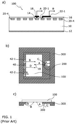
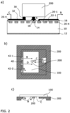
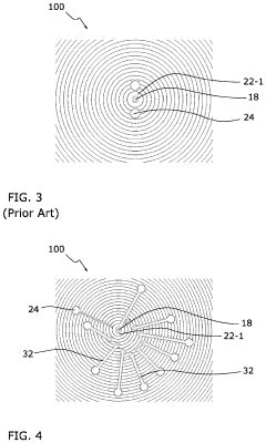
- A hybrid integrated silicon drift detector (HiSDD) is developed, integrating a silicon drift detector with a low-noise preamplifier module using flip chip bonding to minimize electrical capacitance and mechanical instability, replacing wire bonds with stable flip chip connections and using electrically conductive paths for other connections to simplify the bonding process.
Wavelength dispersive x-ray spectrometer
PatentWO2019236384A1
Innovation
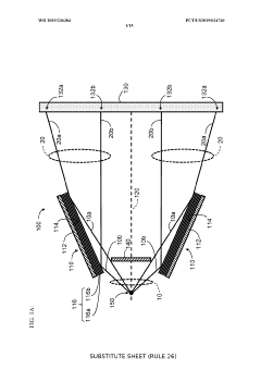
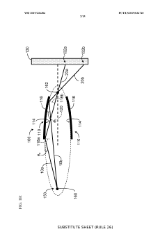
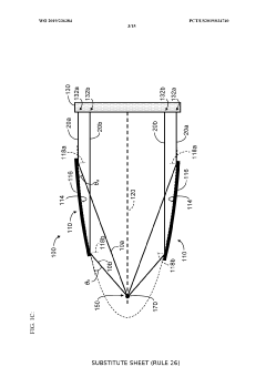
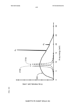
- The development of an x-ray spectrometer with a multilayer stack or mosaic crystal structure that allows for parallel detection of x-rays of different wavelengths, enabling simultaneous recording of an entire x-ray spectrum or spectral segments by using a substrate with varying surface geometry and alternating layers to diffract and spatially separate x-rays based on energy, as per the Bragg relation.
Standardization and Calibration Protocols
Standardization and calibration protocols are essential for ensuring the reliability and reproducibility of SEM-EDS analyses, particularly when dealing with spectral overlaps. These protocols establish the foundation for accurate peak deconvolution and artifact identification in electron microscopy spectroscopy.
The primary calibration procedure involves energy calibration, which must be performed regularly using certified reference materials with well-defined peak positions. This calibration ensures that the energy scale of the EDS system accurately corresponds to specific elemental emissions, facilitating proper identification of overlapping peaks. Most modern systems require calibration using at least two reference points, typically Mn Kα (5.894 keV) and Cu Kα (8.040 keV), to establish both offset and gain parameters.
Resolution calibration represents another critical aspect, measuring the detector's ability to distinguish between closely spaced peaks. The industry standard involves measuring the full width at half maximum (FWHM) of the Mn Kα peak at 5.9 keV. Modern silicon drift detectors (SDDs) typically achieve 125-130 eV resolution, which must be regularly verified to ensure optimal performance for peak deconvolution applications.
Quantitative analysis requires intensity calibration using matrix-matched standards. For elements prone to spectral overlaps, such as Ti-V, Ba-Ti, or S-Mo, specialized standards containing known concentrations of these element pairs are essential. The calibration curves must account for the non-linear relationship between X-ray intensity and concentration, particularly at low concentrations where peak overlaps become more problematic.
Cross-laboratory validation protocols have been established by organizations such as ASTM International and ISO to ensure consistency across different instruments and laboratories. These protocols specify minimum requirements for calibration frequency, acceptable drift parameters, and verification procedures using secondary standards. Adherence to these standards is particularly important when WDS cross-checks are employed to verify EDS results in cases of significant spectral overlaps.
Artifact identification requires specialized calibration procedures to characterize system-specific phenomena such as escape peaks, sum peaks, and silicon internal fluorescence. These artifacts must be systematically documented using reference materials to create instrument-specific artifact libraries that can be referenced during routine analysis to prevent misidentification of overlapping peaks.
Automated calibration verification software has become increasingly important, with modern systems implementing daily verification routines that track detector performance over time. These systems generate control charts that can identify gradual degradation in resolution or energy calibration before they significantly impact spectral deconvolution capabilities.
Data Processing Algorithms and AI Integration
The evolution of data processing algorithms for SEM-EDS spectral analysis has significantly advanced the field's capabilities in addressing peak overlaps and artifacts. Traditional deconvolution methods relied on linear least squares fitting and reference spectra comparison, which often struggled with complex overlapping peaks common in transition metals and rare earth elements.
Recent algorithmic innovations have introduced adaptive peak fitting models that dynamically adjust to spectral characteristics, improving separation of closely positioned peaks. These algorithms incorporate physical models of X-ray generation and detection processes, enabling more accurate quantification even when K, L, and M lines from different elements overlap significantly.
Machine learning approaches have emerged as powerful tools for spectral processing, with convolutional neural networks (CNNs) demonstrating particular efficacy in pattern recognition within complex spectra. Deep learning models trained on extensive spectral libraries can now identify subtle features that traditional algorithms might miss, especially in low-concentration elements where signal-to-noise ratios are challenging.
AI integration has revolutionized artifact identification and correction processes. Supervised learning algorithms can now automatically detect and compensate for common artifacts such as sum peaks, escape peaks, and silicon internal fluorescence effects that previously required expert manual intervention. This automation has significantly reduced analysis time while improving consistency across operators.
Transfer learning techniques have enabled the adaptation of pre-trained neural networks to specific analytical challenges, allowing laboratories to customize solutions for their particular sample types with minimal additional training data. This approach has proven especially valuable for specialized industries dealing with unique material compositions.
Real-time processing capabilities have advanced through the implementation of GPU-accelerated algorithms, enabling instantaneous spectral deconvolution during mapping operations. This development has transformed workflow efficiency, allowing analysts to make immediate decisions about additional measurements or sample preparation adjustments.
Federated learning frameworks are beginning to emerge, allowing multiple institutions to collaboratively improve spectral processing algorithms without sharing sensitive sample data. This collaborative approach accelerates the development of robust solutions for challenging spectral overlap scenarios while maintaining data privacy and intellectual property protections.
Integration with cloud computing platforms has expanded computational capabilities beyond local hardware limitations, enabling more sophisticated processing algorithms to be deployed even on standard laboratory equipment. This democratization of advanced processing capabilities is reducing the expertise barrier for high-quality elemental analysis across diverse research and industrial applications.
Unlock deeper insights with Patsnap Eureka Quick Research — get a full tech report to explore trends and direct your research. Try now!
Generate Your Research Report Instantly with AI Agent
Supercharge your innovation with Patsnap Eureka AI Agent Platform!
