SEM-EDS Mapping Strategy: Pixel Size, Frame Summation And Drift Correction
SEP 22, 20259 MIN READ
Generate Your Research Report Instantly with AI Agent
Patsnap Eureka helps you evaluate technical feasibility & market potential.
SEM-EDS Mapping Evolution and Objectives
Scanning Electron Microscopy coupled with Energy Dispersive X-ray Spectroscopy (SEM-EDS) has evolved significantly since its inception in the 1960s. Initially, EDS mapping was limited by slow acquisition speeds and poor spatial resolution, restricting its application to basic elemental identification. The 1980s marked a turning point with the introduction of silicon drift detectors (SDDs), which dramatically improved count rates and energy resolution, enabling faster and more accurate elemental mapping.
The 1990s witnessed the integration of digital imaging systems, allowing for the correlation of elemental maps with high-resolution SEM images. This period also saw the development of the first automated drift correction algorithms, addressing a critical limitation in long-duration mapping sessions. By the early 2000s, multi-detector systems emerged, significantly enhancing collection efficiency and enabling true quantitative mapping capabilities.
Recent advancements have focused on optimizing three critical parameters: pixel size, frame summation, and drift correction. Pixel size determination has evolved from arbitrary selection to sophisticated algorithms that balance spatial resolution with signal-to-noise ratio. Modern systems now incorporate adaptive pixel sizing that adjusts based on sample characteristics and desired analytical outcomes.
Frame summation techniques have progressed from simple averaging to weighted statistical methods that maximize signal quality while minimizing beam damage. Contemporary systems employ intelligent frame integration algorithms that can identify and exclude anomalous frames, resulting in cleaner, more representative elemental maps.
Drift correction has seen perhaps the most dramatic improvement, evolving from manual reference point selection to real-time, AI-driven correction systems. Current technologies can compensate for thermal, mechanical, and charge-induced drift with sub-nanometer precision, enabling extended mapping sessions without loss of spatial registration.
The primary objective of modern SEM-EDS mapping is to achieve the optimal balance between spatial resolution, elemental sensitivity, and acquisition time. This involves developing strategies that maximize information content while minimizing beam damage and drift effects. Secondary objectives include enhancing quantification accuracy through improved background modeling and peak deconvolution algorithms.
Looking forward, the field aims to push the boundaries of detection limits and spatial resolution simultaneously. This includes developing new detector geometries, improving count statistics through novel signal processing, and implementing machine learning approaches for automated feature recognition and classification in complex multi-element maps.
Market Applications and Demand Analysis for SEM-EDS Mapping
The SEM-EDS mapping technology market has experienced significant growth over the past decade, driven by increasing demand across multiple industries requiring advanced material characterization capabilities. The global market for electron microscopy, which includes SEM-EDS systems, was valued at approximately $4.1 billion in 2022 and is projected to grow at a CAGR of 8.2% through 2030, with SEM-EDS mapping solutions representing a substantial segment of this market.
Materials science and semiconductor industries remain the primary consumers of SEM-EDS mapping technology, collectively accounting for over 45% of the total market share. The semiconductor industry, in particular, demonstrates an escalating need for high-resolution elemental mapping to support quality control in increasingly miniaturized chip manufacturing processes, where precise pixel size optimization and drift correction are critical for accurate defect analysis.
The automotive and aerospace sectors represent rapidly expanding markets for SEM-EDS mapping applications, particularly in failure analysis and quality assurance of advanced materials and components. These industries require enhanced mapping strategies with superior drift correction capabilities to analyze complex alloys and composite materials under various environmental conditions.
Healthcare and pharmaceutical industries have emerged as significant growth sectors, utilizing SEM-EDS mapping for drug delivery systems, implant materials analysis, and nanoparticle characterization. These applications demand sophisticated frame summation techniques to enhance signal-to-noise ratios when analyzing biological samples with low elemental concentrations.
Environmental monitoring and forensic science applications are creating new market opportunities, with a growing demand for portable or field-deployable SEM-EDS systems that can maintain mapping accuracy despite challenging operating conditions. This segment is expected to grow at 12% annually, outpacing the overall market growth rate.
Geographically, North America and Europe currently dominate the market with approximately 60% combined market share, primarily due to established research infrastructure and industrial bases. However, the Asia-Pacific region is witnessing the fastest growth rate at 10.5% annually, driven by expanding semiconductor manufacturing and materials research activities in China, South Korea, and Taiwan.
Customer surveys indicate that end-users increasingly prioritize mapping accuracy and resolution over acquisition speed, with 78% of respondents identifying drift correction capabilities as "very important" or "critical" in their purchasing decisions. This trend is particularly pronounced in precision-critical applications such as semiconductor failure analysis and advanced materials development.
The market is also witnessing a shift toward integrated solutions that combine optimized pixel size selection, intelligent frame summation, and real-time drift correction in automated workflows, reflecting the growing demand for more accessible and user-friendly SEM-EDS mapping systems across diverse industry applications.
Current Challenges in SEM-EDS Spatial Resolution
Despite significant advancements in SEM-EDS technology, achieving optimal spatial resolution remains a persistent challenge in elemental mapping applications. The fundamental limitation stems from the interaction volume of the electron beam with the sample, which creates a region significantly larger than the beam diameter from which X-rays are generated. This physical constraint fundamentally limits the achievable spatial resolution regardless of the sophistication of the instrumentation.
Current SEM-EDS systems typically achieve spatial resolutions of 0.5-1 μm at best under optimal conditions, which falls short of the nanometer-scale resolution that modern materials science and semiconductor applications increasingly demand. This resolution gap becomes particularly problematic when analyzing nanomaterials, thin films, or complex multilayered structures where elemental distribution at interfaces is critical.
Beam drift during extended acquisition periods presents another significant challenge. As mapping sessions often require several hours to collect sufficient X-ray counts for statistically meaningful results, even minor stage or beam instabilities can severely degrade spatial resolution. Current drift correction algorithms struggle to maintain accuracy over extended periods, especially when sample charging or thermal expansion occurs.
The trade-off between pixel size and acquisition time creates a practical dilemma for researchers. Smaller pixel sizes theoretically improve resolution but require longer dwell times to collect sufficient X-ray counts, increasing the total acquisition time and susceptibility to drift. Conversely, larger pixels with shorter acquisition times sacrifice spatial detail but improve signal-to-noise ratios and reduce drift effects.
Frame summation techniques, while helpful for improving signal quality, introduce their own complications. Misalignment between frames due to drift can actually degrade rather than enhance spatial resolution if not properly corrected. Current software solutions for frame alignment often struggle with low-contrast samples or when significant drift occurs between frames.
Detector limitations further compound these challenges. Even with modern silicon drift detectors (SDDs), the count rate capabilities and energy resolution can become limiting factors when attempting high-resolution mapping with small pixel sizes and short dwell times. The statistical nature of X-ray generation and detection means that achieving both high spatial resolution and good counting statistics remains fundamentally challenging.
Sample-specific issues such as beam damage, charging, and contamination during extended mapping sessions can progressively degrade both image quality and elemental distribution accuracy, particularly in beam-sensitive materials like polymers or biological samples. These effects become more pronounced as pixel size decreases and dwell time increases in pursuit of higher resolution.
Current Frame Summation and Drift Correction Methods
01 Pixel size optimization in SEM-EDS mapping
Optimization of pixel size in SEM-EDS mapping is crucial for achieving high-resolution elemental distribution images. The pixel size determines the spatial resolution of the mapping and should be selected based on the specific requirements of the analysis. Smaller pixel sizes provide higher resolution but may require longer acquisition times and can be more susceptible to beam damage. Advanced algorithms can be used to optimize the pixel size based on the sample characteristics and the desired level of detail in the elemental maps.- Pixel size optimization in SEM-EDS mapping: Optimizing pixel size in SEM-EDS mapping is crucial for achieving high-resolution elemental distribution images. The pixel size determines the spatial resolution of the mapping and should be selected based on the sample characteristics and analytical requirements. Smaller pixel sizes provide higher resolution but may require longer acquisition times and can be more susceptible to beam damage. Advanced systems allow for adaptive pixel sizing based on the specific elements being mapped and the desired signal-to-noise ratio.
- Frame summation techniques for improved signal quality: Frame summation involves acquiring multiple frames of the same area and summing them to improve signal quality in SEM-EDS mapping. This technique enhances the signal-to-noise ratio, allowing for better detection of trace elements and more accurate quantification. The number of frames to be summed depends on the sample stability, beam sensitivity, and required detection limits. Modern systems can perform real-time frame summation with progressive improvement of the elemental maps as more frames are acquired.
- Drift correction methods for long acquisition times: Drift correction is essential for maintaining spatial accuracy during long SEM-EDS mapping acquisitions. Sample or beam drift can cause blurring and misalignment of elemental maps. Advanced systems employ various drift correction algorithms, including feature tracking, cross-correlation between successive frames, and reference marker methods. Real-time drift correction continuously monitors and adjusts for positional changes, while post-acquisition drift correction aligns frames before summation. These methods ensure that spatial relationships between elements are accurately preserved even during extended mapping sessions.
- Integration of image processing algorithms for enhanced mapping: Advanced image processing algorithms significantly enhance the quality and information content of SEM-EDS maps. These include background subtraction, peak deconvolution, and noise reduction techniques. Machine learning and AI-based approaches can identify patterns and correlations in elemental distributions that might not be apparent through conventional analysis. Multivariate statistical methods such as principal component analysis help separate overlapping elemental signatures and identify phases based on their characteristic elemental compositions.
- 3D elemental mapping and tomographic reconstruction: Three-dimensional SEM-EDS mapping techniques provide depth-resolved elemental information by combining serial sectioning or focused ion beam milling with EDS mapping. These methods require precise alignment between successive layers and specialized reconstruction algorithms to create accurate 3D elemental distribution models. Challenges include maintaining consistent analytical conditions throughout the volume acquisition and correcting for absorption effects at different depths. Advanced software tools enable visualization and quantitative analysis of elemental distributions in three dimensions.
02 Frame summation techniques for improved signal-to-noise ratio
Frame summation involves acquiring multiple frames of the same area and summing them to improve the signal-to-noise ratio in SEM-EDS mapping. This technique is particularly useful for samples with low elemental concentrations or when high-speed mapping is required. By summing multiple frames, the random noise is averaged out while the signal is enhanced, resulting in clearer elemental distribution maps. Advanced frame summation algorithms can also compensate for slight variations between frames, further improving the quality of the final map.Expand Specific Solutions03 Drift correction methods for high-resolution mapping
Drift correction is essential for maintaining spatial accuracy during long SEM-EDS mapping sessions. Sample or beam drift can cause distortion and blurring in elemental maps, particularly at high magnifications or during extended acquisition times. Advanced drift correction methods use reference features or patterns to track and compensate for drift in real-time or during post-processing. These methods can involve image registration algorithms, correlation techniques, or dedicated hardware solutions to ensure that the spatial information in the elemental maps remains accurate throughout the acquisition process.Expand Specific Solutions04 Integration of image processing algorithms for enhanced mapping quality
Advanced image processing algorithms can significantly enhance the quality of SEM-EDS elemental maps. These algorithms can include denoising filters, contrast enhancement, background subtraction, and peak deconvolution techniques. By applying these processing methods, researchers can extract more information from the raw data, improve the visualization of elemental distributions, and facilitate quantitative analysis. Machine learning and artificial intelligence approaches are increasingly being used to automate and optimize these image processing steps, making high-quality elemental mapping more accessible and reproducible.Expand Specific Solutions05 Real-time data acquisition and processing systems
Real-time data acquisition and processing systems enable immediate visualization and analysis of SEM-EDS mapping data. These systems integrate hardware and software components to collect, process, and display elemental maps as they are being acquired. Real-time processing can include drift correction, frame summation, and preliminary quantification, allowing researchers to make adjustments to acquisition parameters on the fly. This approach is particularly valuable for time-sensitive analyses or when working with beam-sensitive samples where minimizing exposure time is critical.Expand Specific Solutions
Leading Manufacturers and Research Institutions
The SEM-EDS mapping technology market is currently in a growth phase, with increasing demand for advanced materials characterization in semiconductor, electronics, and materials science sectors. The market size is expanding steadily as industries require higher resolution and more accurate elemental analysis capabilities. Technologically, the field is maturing with innovations focusing on optimizing pixel size parameters, frame summation techniques, and drift correction algorithms. Leading players include established equipment manufacturers like Hitachi High-Tech America, Oxford Instruments NanoTechnology Tools, and FEI Co. (now part of Thermo Fisher), alongside research-driven entities such as Samsung Electronics and ASML Netherlands. Academic institutions like Huazhong University of Science & Technology and University of Florida are contributing significant research advancements, while semiconductor giants like KIOXIA and Seagate are driving application-specific developments to meet increasing demands for nanoscale analysis precision.
Hitachi High-Tech America, Inc.
Technical Solution: Hitachi High-Tech has pioneered innovative SEM-EDS mapping strategies focusing on optimizing pixel size, frame summation, and drift correction. Their SU7000 series implements an advanced Real-time 3D Drift Correction system that continuously monitors sample movement in all three dimensions, automatically adjusting the electron beam position up to 60 times per second to maintain precise spatial registration[1]. For pixel size optimization, Hitachi employs their proprietary "Smart Mapping" technology that dynamically adjusts pixel dimensions based on the specific elements being analyzed and their expected distribution, with capabilities ranging from 2nm to 500nm to balance resolution and acquisition speed[2]. Their frame summation approach utilizes a weighted statistical algorithm that intelligently combines multiple frames while accounting for signal-to-noise variations across the energy spectrum. This system can process up to 4096 frames per map with automatic outlier rejection to eliminate artifacts from random noise events. Hitachi's latest systems also incorporate machine learning algorithms that predict and compensate for both mechanical and electronic drift factors, reducing distortion by up to 75% compared to conventional methods during extended mapping sessions[3].
Strengths: Exceptional drift correction capabilities suitable for long-duration mapping; adaptive pixel sizing optimizes resolution for specific elements; advanced statistical processing of frame data improves signal quality. Weaknesses: Proprietary software ecosystem can limit integration with third-party analysis tools; high-end systems require significant capital investment; some automated optimization features reduce manual control options for specialized applications.
Oxford Instruments NanoTechnology Tools Ltd.
Technical Solution: Oxford Instruments has developed comprehensive SEM-EDS mapping solutions through their AZtec platform, specifically addressing pixel size optimization, frame summation, and drift correction challenges. Their TruMap™ technology implements an adaptive pixel sizing algorithm that automatically determines optimal spatial resolution based on the specific elements being mapped and their expected distribution characteristics[1]. For high-precision applications, the system can achieve pixel resolutions down to 1-2 nm while maintaining count statistics through intelligent dwell time management. Oxford's frame summation approach employs their proprietary AutoLock+ drift correction system, which operates in real-time during acquisition by tracking reference features across multiple frames and applying spatial transformations to maintain perfect alignment[2]. This system can correct for both linear and non-linear drift components, reducing spatial distortion by up to 90% during extended mapping sessions. Their latest innovation, LayerProbe™, extends these capabilities to 3D elemental mapping by incorporating Z-axis drift correction between sequential layers. For challenging samples with beam-sensitive materials, Oxford has implemented a dose-fractionation approach that distributes electron exposure across multiple rapid scans, with sophisticated signal processing algorithms that can extract meaningful elemental data from individually noisy frames when combined[3].
Strengths: Industry-leading drift correction capabilities; sophisticated adaptive algorithms for pixel size optimization; excellent integration with quantitative analysis tools. Weaknesses: Complex system requires significant training to fully utilize advanced features; premium pricing model; some automated workflows may limit flexibility for highly specialized research applications.
Key Patents in SEM-EDS Mapping Technology
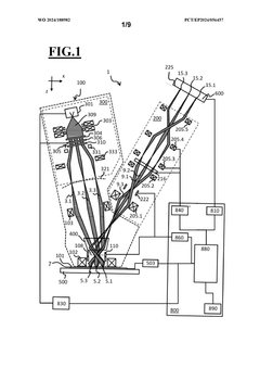
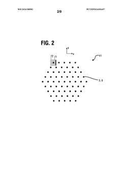
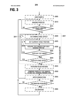
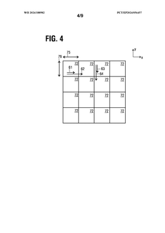
Monitoring of imaging parameters of scanning electron microscopy
PatentWO2024188982A1
Innovation
- A method for monitoring multi-beam scanning electron imaging systems by acquiring pairs of test images at different stage positions to determine imaging parameters such as distortion, allowing for self-calibration without the need for separate calibration samples, using program code to execute the method and adjust control signals for correction.
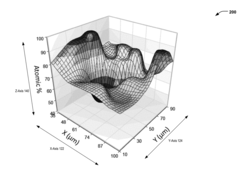
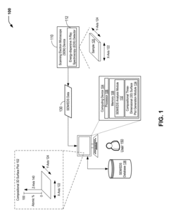
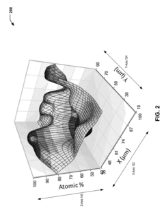
Compositional three-dimensional surface plots
PatentInactiveUS20170329936A1
Innovation
- A method and system that utilize SEM/EDS data to generate compositional three-dimensional surface plots, where the Z-axis represents atomic or weight percentage composition, enabling quantitative data visualization for each location of a sample, by receiving and processing data from a scanning electron microscope equipped with an EDS detector.
Data Processing Algorithms for SEM-EDS Maps
The processing of SEM-EDS mapping data requires sophisticated algorithms to transform raw spectral information into meaningful elemental distribution maps. These algorithms must address several key challenges inherent to the acquisition process, including noise reduction, spectral deconvolution, and drift compensation.
Spectral deconvolution algorithms form the foundation of EDS data processing, separating overlapping elemental peaks to accurately identify and quantify elements present in each pixel. Modern approaches employ mathematical models such as Gaussian peak fitting and background subtraction methods to isolate individual elemental contributions from the complex spectral data.
Noise reduction algorithms are critical for enhancing signal-to-noise ratios, particularly in low-count scenarios or when mapping trace elements. Advanced techniques include wavelet transforms, principal component analysis (PCA), and various filtering methods that preserve spatial features while minimizing random fluctuations in the spectral data.
Drift correction algorithms compensate for specimen movement during extended mapping sessions, which can cause spatial distortion in the resulting elemental maps. Cross-correlation techniques compare successive frames to detect and correct positional shifts, while more advanced methods incorporate machine learning approaches to predict and compensate for complex drift patterns.
Frame summation algorithms intelligently combine multiple scans of the same area to improve counting statistics without sacrificing spatial resolution. These algorithms must account for potential drift between frames and apply appropriate weighting based on signal quality metrics.
Quantification algorithms convert X-ray intensity data into meaningful concentration values, considering matrix effects, absorption phenomena, and fluorescence effects. ZAF correction methods and fundamental parameter approaches are commonly employed to achieve accurate quantitative results across diverse sample compositions.
Visualization enhancement algorithms transform processed data into visually interpretable maps, applying color mapping, contrast enhancement, and overlay techniques to highlight elemental distributions. Recent developments include adaptive color scales that optimize visibility of both major and trace elements within the same visualization.
Real-time processing algorithms have emerged with increasing computational power, enabling on-the-fly data processing during acquisition. These algorithms provide immediate feedback on mapping quality and can adaptively adjust acquisition parameters to optimize results for specific regions of interest.
Sample Preparation Impact on Mapping Quality
Sample preparation plays a critical role in determining the quality and reliability of SEM-EDS mapping results. The physical and chemical characteristics of the specimen surface directly influence electron beam interaction, X-ray generation, and ultimately the accuracy of elemental distribution maps.
Surface flatness represents one of the most significant preparation factors affecting mapping quality. Uneven surfaces create topographical contrast that can be misinterpreted as compositional variations. When the electron beam strikes an inclined surface, the interaction volume changes shape and size, altering X-ray generation and detection efficiency. This effect becomes particularly problematic when mapping at high magnifications with small pixel sizes, as surface irregularities can introduce systematic errors in elemental quantification.
Contamination control during sample preparation significantly impacts mapping outcomes. Residual polishing compounds, fingerprints, or environmental contaminants can introduce spurious elemental signals that obscure genuine compositional features. Carbon-based contaminants are especially problematic as they can accumulate under electron beam exposure, creating artifacts that evolve during extended mapping sessions and compromising drift correction algorithms.
The electrical conductivity of samples, determined by preparation methods, affects charging phenomena during mapping. Poorly conductive specimens experience charge accumulation that deflects the electron beam, causing distortion in mapping patterns. While conductive coatings mitigate this issue, they simultaneously attenuate low-energy X-rays, potentially masking light elements. The coating thickness must be optimized to balance charge dissipation against X-ray attenuation.
Sample homogeneity at the microscale influences mapping strategy decisions. Heterogeneous materials with fine-scale features require smaller pixel sizes and longer dwell times to resolve compositional boundaries accurately. Preparation techniques that introduce artificial heterogeneity, such as smearing of soft phases during polishing, can necessitate adjustments to mapping parameters.
The crystallographic orientation of grains, revealed through preparation techniques like etching, affects electron channeling and consequently X-ray generation efficiency. This crystallographic contrast can introduce apparent compositional variations in maps of single-phase materials. Understanding these effects is essential when interpreting mapping data, particularly when frame summation is employed to enhance signal-to-noise ratios.
Ultimately, optimized sample preparation protocols must be developed specifically for SEM-EDS mapping applications, considering the unique requirements of spatial resolution, elemental sensitivity, and drift correction capabilities of modern systems.
Unlock deeper insights with Patsnap Eureka Quick Research — get a full tech report to explore trends and direct your research. Try now!
Generate Your Research Report Instantly with AI Agent
Supercharge your innovation with Patsnap Eureka AI Agent Platform!