

Signal Integrity vs Via Structures
MAR 26, 20269 MIN READ
Generate Your Research Report Instantly with AI Agent
Patsnap Eureka helps you evaluate technical feasibility & market potential.
Signal Integrity Via Design Background and Objectives
Signal integrity has emerged as one of the most critical challenges in modern electronic design, particularly as digital systems continue to push the boundaries of speed, density, and performance. The exponential growth in data rates, from gigahertz to multi-gigahertz frequencies, has transformed what were once negligible parasitic effects into dominant factors that can make or break system functionality. In this high-speed digital landscape, every interconnect element becomes a potential source of signal degradation, timing uncertainty, and electromagnetic interference.
Via structures represent a fundamental yet often underestimated component in this signal integrity equation. As the essential vertical interconnects in multilayer printed circuit boards, vias serve as the critical pathways that enable signals to traverse between different routing layers. However, their seemingly simple cylindrical geometry belies a complex electromagnetic behavior that can introduce significant impedance discontinuities, crosstalk, and signal reflections when not properly designed and optimized.
The relationship between signal integrity and via structures has evolved from a secondary design consideration to a primary engineering constraint. Traditional via design approaches, which primarily focused on mechanical reliability and basic electrical connectivity, are no longer sufficient for contemporary high-speed applications. The parasitic inductance, capacitance, and resistance introduced by via structures can cause signal distortion, increased jitter, and reduced noise margins that directly impact system performance and reliability.
Modern electronic systems demand unprecedented levels of signal fidelity across increasingly complex routing architectures. Multi-gigabit serial interfaces, high-speed memory systems, and advanced processor interconnects all rely on via structures that must maintain signal integrity while accommodating dense routing requirements. The challenge is further compounded by the need to support differential signaling, minimize electromagnetic interference, and ensure robust performance across varying environmental conditions.
The primary objective of advanced via design methodologies is to develop comprehensive solutions that minimize signal integrity degradation while maintaining manufacturing feasibility and cost effectiveness. This involves creating via structures that exhibit controlled impedance characteristics, reduced parasitic effects, and optimized electromagnetic performance across the entire frequency spectrum of interest. Additionally, the design approach must address the complex interactions between via geometry, surrounding copper structures, and dielectric materials to achieve predictable and repeatable electrical behavior.
Market Demand for High-Speed PCB Via Solutions
The global electronics industry is experiencing unprecedented demand for high-speed PCB via solutions, driven by the exponential growth in data transmission requirements across multiple sectors. Consumer electronics, telecommunications infrastructure, automotive systems, and data center equipment are pushing the boundaries of signal integrity performance, creating substantial market opportunities for advanced via technologies.
5G network deployment represents one of the most significant demand drivers, requiring PCBs capable of handling frequencies exceeding 28 GHz while maintaining signal fidelity. Base stations, small cells, and mobile devices demand sophisticated via structures that minimize insertion loss and crosstalk. The automotive sector's transition toward autonomous vehicles and electric powertrains further amplifies this demand, as advanced driver assistance systems and high-speed communication networks require robust signal integrity solutions.
Data center modernization initiatives are creating substantial market pull for high-performance via technologies. Cloud computing providers and enterprise customers are upgrading infrastructure to support higher bandwidth applications, artificial intelligence workloads, and edge computing deployments. These applications demand PCBs with via structures capable of supporting multi-gigabit data rates while maintaining thermal stability and mechanical reliability.
The consumer electronics segment continues to drive volume demand, particularly in smartphones, tablets, and wearable devices where miniaturization constraints require innovative via solutions. High-resolution displays, advanced camera systems, and wireless charging capabilities necessitate PCBs with optimized via structures that balance performance with space efficiency.
Industrial automation and Internet of Things applications are emerging as significant growth areas, requiring reliable high-speed connectivity in harsh operating environments. Manufacturing equipment, robotics systems, and sensor networks demand via solutions that maintain signal integrity across extended temperature ranges and mechanical stress conditions.
Market dynamics indicate strong preference for via technologies that offer design flexibility, manufacturing scalability, and cost-effectiveness. Companies are increasingly seeking solutions that can accommodate multiple signal types, support dense routing requirements, and integrate seamlessly with existing manufacturing processes while delivering measurable improvements in signal integrity performance.
Current Via Structure SI Challenges and Limitations
Modern high-speed electronic systems face increasingly complex signal integrity challenges as via structures become critical bottlenecks in maintaining signal quality. Traditional through-hole vias, while providing reliable interconnection between PCB layers, introduce significant parasitic effects that severely impact signal transmission at frequencies above 10 GHz. The inherent inductance and capacitance of these structures create impedance discontinuities, leading to signal reflections, crosstalk, and power delivery network instabilities.
Stub resonance represents one of the most persistent challenges in current via designs. When signals traverse multi-layer PCBs, unused via segments below the target layer act as open-ended transmission lines, creating resonant frequencies that cause severe signal distortion. These stub effects become particularly problematic in high-speed digital applications where signal rise times approach picosecond ranges, making traditional via structures inadequate for next-generation systems operating beyond 25 Gbps data rates.
Impedance control difficulties plague conventional via structures due to their cylindrical geometry and surrounding dielectric variations. The transition from planar transmission lines to three-dimensional via structures creates unavoidable impedance mismatches, typically ranging from 30-60 ohms compared to the standard 50-ohm characteristic impedance. This mismatch becomes more pronounced as via aspect ratios increase, particularly in thick PCB stackups required for complex multilayer designs.
Manufacturing limitations further constrain via performance optimization. Current PCB fabrication processes struggle to maintain consistent via barrel plating thickness, leading to impedance variations across production lots. The minimum achievable via diameter and drill accuracy limitations prevent the implementation of optimal via geometries that could minimize parasitic effects. Additionally, the inability to precisely control dielectric properties around via structures introduces unpredictable variations in signal propagation characteristics.
Crosstalk mitigation remains inadequately addressed in conventional via designs. Dense via fields required for high pin-count components create electromagnetic coupling between adjacent signal paths, resulting in near-end and far-end crosstalk that degrades signal integrity margins. Current shielding techniques using ground vias provide limited effectiveness while consuming valuable routing resources and increasing manufacturing complexity.
Power delivery network integrity suffers from via-induced voltage fluctuations and ground bounce effects. The parasitic inductance of power and ground vias creates impedance paths that cannot adequately suppress high-frequency switching noise, leading to simultaneous switching noise and power supply voltage variations that affect overall system performance and electromagnetic compatibility.
Existing Via Structure Solutions for SI Optimization
01 Via structure design and geometry optimization
Optimizing the physical design and geometry of via structures is critical for maintaining signal integrity. This includes controlling via diameter, aspect ratio, pad size, and anti-pad dimensions to minimize impedance discontinuities and reduce signal reflections. Proper via geometry helps maintain controlled impedance throughout the signal path and reduces parasitic capacitance and inductance that can degrade signal quality.- Via structure design and geometry optimization: Optimizing the physical design and geometry of via structures is crucial for maintaining signal integrity. This includes controlling via diameter, length, pad size, and anti-pad dimensions to minimize impedance discontinuities and reduce signal reflections. Proper via geometry helps maintain controlled impedance throughout the signal path and reduces parasitic capacitance and inductance that can degrade signal quality.
- Via stub reduction and back-drilling techniques: Via stubs can cause signal reflections and resonance issues at high frequencies, degrading signal integrity. Techniques such as back-drilling, blind vias, and buried vias are employed to minimize or eliminate stub lengths. These methods help reduce impedance mismatches and improve signal transmission quality, particularly in high-speed digital applications where stub resonances can significantly impact performance.
- Via shielding and ground via placement: Strategic placement of ground vias around signal vias provides electromagnetic shielding and reduces crosstalk between adjacent signal paths. Ground via fencing creates a low-impedance return path and helps contain electromagnetic fields, preventing interference. This technique is particularly important in high-density interconnect designs where multiple signal vias are in close proximity and mutual coupling can degrade signal integrity.
- Differential via pair design and symmetry: For differential signaling applications, maintaining symmetry and matched characteristics between via pairs is essential for preserving signal integrity. This includes ensuring equal via lengths, matched impedances, and symmetric routing to minimize skew and common-mode noise. Proper differential via design helps maintain the benefits of differential signaling, including improved noise immunity and reduced electromagnetic interference.
- Via transition modeling and simulation: Accurate electromagnetic modeling and simulation of via transitions is critical for predicting and optimizing signal integrity performance. This involves using electromagnetic field solvers to analyze via structures, extract equivalent circuit models, and predict their impact on signal transmission. Simulation enables designers to identify potential signal integrity issues early in the design process and optimize via structures before fabrication, reducing design iterations and improving overall performance.
02 Via stub reduction and back-drilling techniques
Via stubs act as resonant structures that can cause signal reflections and degrade high-frequency signal integrity. Techniques such as back-drilling, blind vias, and buried vias are employed to minimize or eliminate stub lengths. These methods remove unused portions of the via barrel below the last connected layer, thereby reducing resonance effects and improving signal transmission characteristics at high frequencies.Expand Specific Solutions03 Ground via placement and shielding structures
Strategic placement of ground vias adjacent to signal vias provides return path continuity and electromagnetic shielding. Ground via fencing and coaxial via structures help contain electromagnetic fields, reduce crosstalk between adjacent signal paths, and minimize electromagnetic interference. Proper ground via distribution ensures low-impedance return paths and improves overall signal integrity by reducing ground bounce and simultaneous switching noise.Expand Specific Solutions04 Via transition impedance matching
Impedance discontinuities at via transitions can cause signal reflections and power loss. Techniques for impedance matching include adjusting anti-pad sizes, using tapered vias, implementing via pads with specific dimensions, and employing compensation structures. These methods ensure smooth impedance transitions between transmission lines and vias, maintaining signal integrity across layer transitions and minimizing return loss at high frequencies.Expand Specific Solutions05 Via array and differential pair via configurations
For high-speed differential signaling and dense interconnect requirements, specialized via configurations are employed. This includes symmetrical via placement for differential pairs to maintain balanced signal propagation, via arrays for power delivery with reduced inductance, and optimized via spacing to minimize crosstalk. These configurations ensure signal integrity in complex multi-layer printed circuit boards while supporting high data rates and maintaining electromagnetic compatibility.Expand Specific Solutions
Key Players in PCB Via and SI Industry
The signal integrity versus via structures technology landscape represents a mature yet rapidly evolving sector driven by increasing demand for high-speed electronic systems and advanced packaging solutions. The market demonstrates substantial growth potential, particularly in 5G infrastructure, data centers, and high-performance computing applications. Technology maturity varies significantly across market participants, with established semiconductor leaders like Intel, Samsung Electronics, Taiwan Semiconductor Manufacturing, and MediaTek driving advanced via design innovations for next-generation processors. Network infrastructure companies including Huawei, Ericsson, and Cisco Technology focus on optimizing signal integrity for telecommunications equipment. Manufacturing specialists such as Hon Hai Precision Industry and Sanmina provide implementation expertise, while emerging players like BOE Technology Group and Chinese firms including Inspur contribute specialized solutions. The competitive landscape reflects a mix of mature technologies in traditional applications and cutting-edge developments in emerging high-frequency domains.
Xilinx, Inc.
Technical Solution: Xilinx addresses signal integrity challenges in via structures through FPGA packaging and PCB design methodologies. Their approach focuses on optimizing via transitions for high-speed differential signals commonly used in FPGA applications. Xilinx implements controlled impedance via design techniques to maintain signal integrity across multiple PCB layers, utilizing electromagnetic simulation tools to model via behavior at gigahertz frequencies. They employ via optimization strategies including proper via placement relative to reference planes and implementation of via fencing techniques to reduce crosstalk between adjacent signal paths. Xilinx's methodology includes comprehensive design rules for via aspect ratios, pad sizes, and anti-pad dimensions to minimize parasitic effects. Their signal integrity approach incorporates advanced packaging technologies with optimized via structures in BGA substrates, ensuring reliable signal transmission from die to PCB level through carefully designed via transitions.
Strengths: Deep expertise in high-speed digital design, strong FPGA application knowledge, comprehensive design tools. Weaknesses: Solutions primarily focused on FPGA applications, may not cover broader signal integrity challenges.
Huawei Technologies Co., Ltd.
Technical Solution: Huawei has developed sophisticated signal integrity solutions for via structures in telecommunications and networking equipment. Their methodology encompasses multi-layer PCB design optimization with focus on via placement strategies to minimize signal degradation in high-speed digital circuits. Huawei implements differential via routing techniques with controlled impedance matching to maintain signal quality across layer transitions. They employ advanced simulation tools for electromagnetic field analysis to predict via behavior at frequencies up to several gigahertz. Their approach includes via stitching techniques for improved ground plane continuity and reduced electromagnetic interference. Huawei's signal integrity design incorporates via optimization algorithms that consider factors such as via diameter, drill depth, and pad sizes to minimize reflections and crosstalk. They utilize blind and buried via technologies in multilayer designs to reduce signal path lengths and improve overall system performance.
Strengths: Extensive experience in high-frequency telecommunications, strong simulation capabilities, comprehensive system-level approach. Weaknesses: Solutions may be proprietary and less accessible to external customers.
Core Innovations in Via Design for Signal Integrity
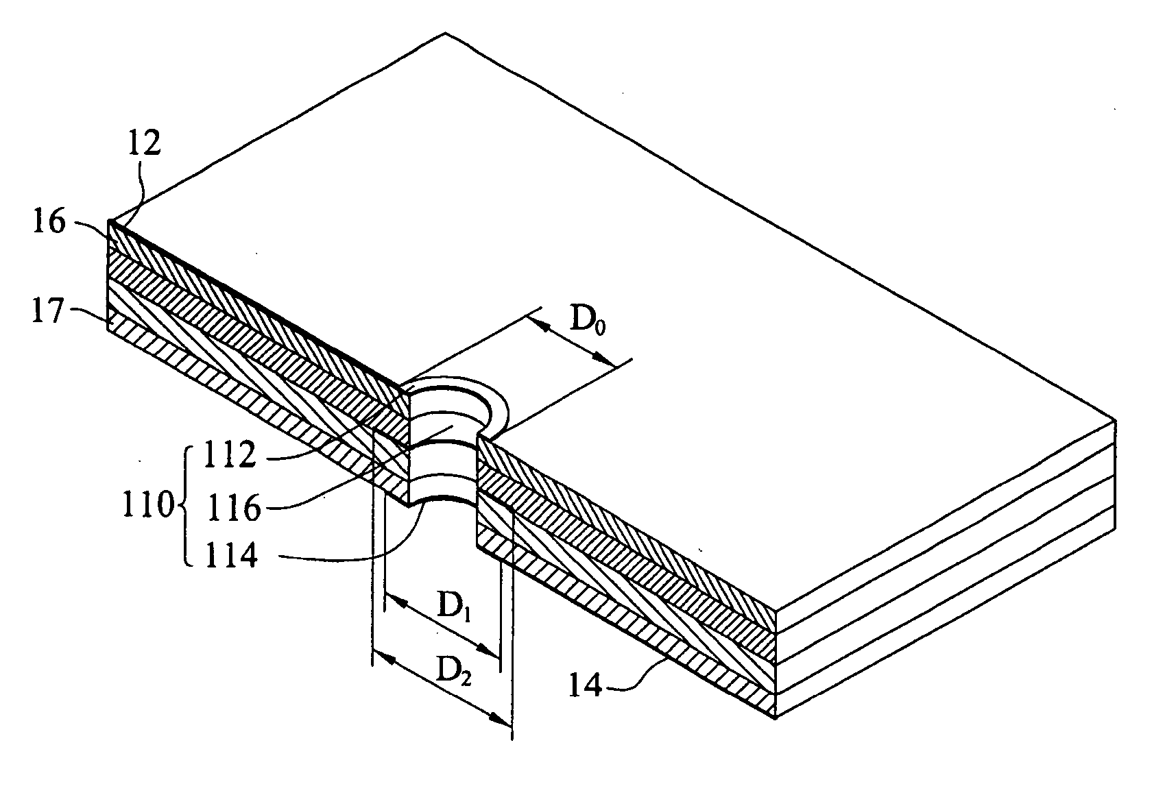
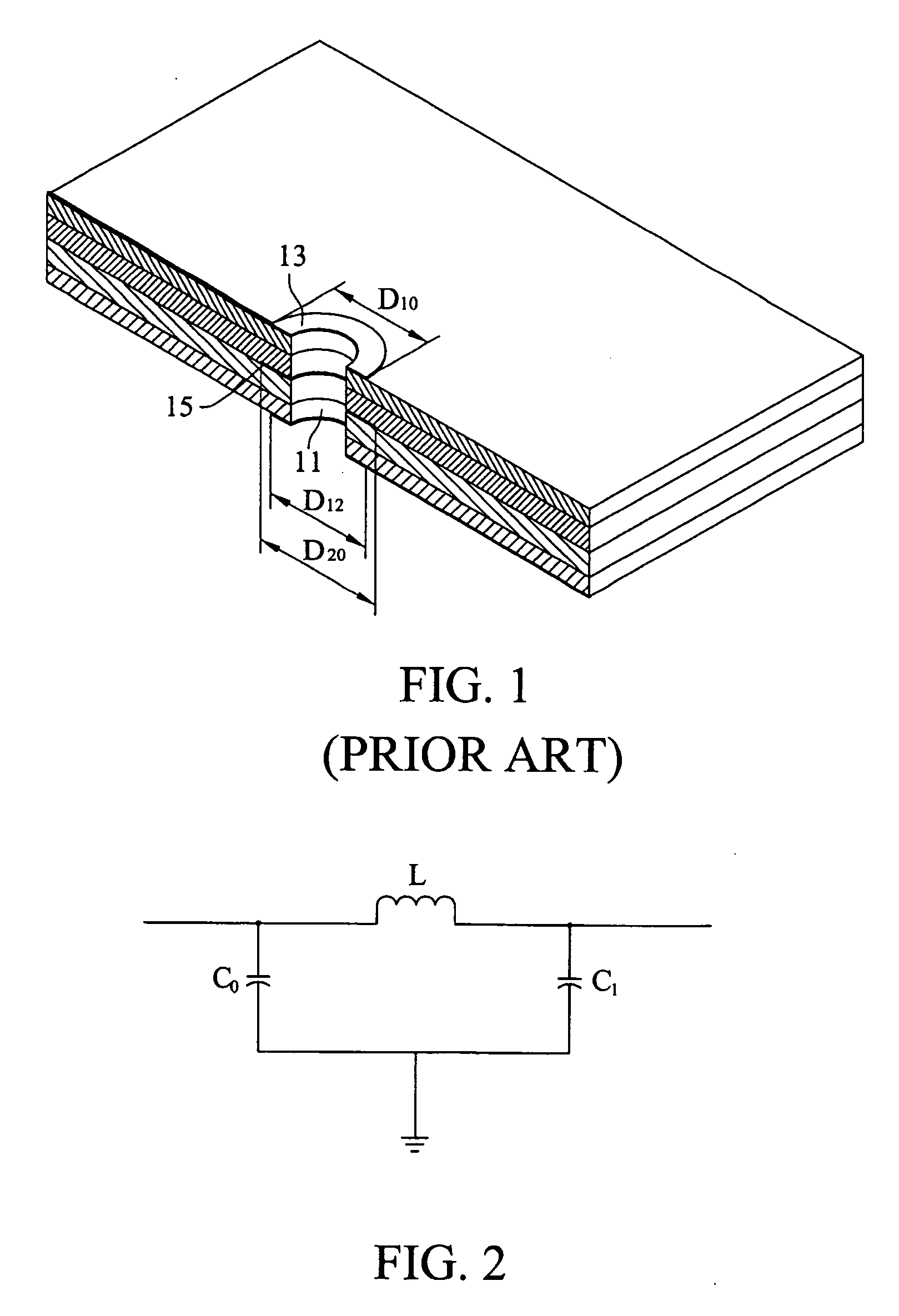
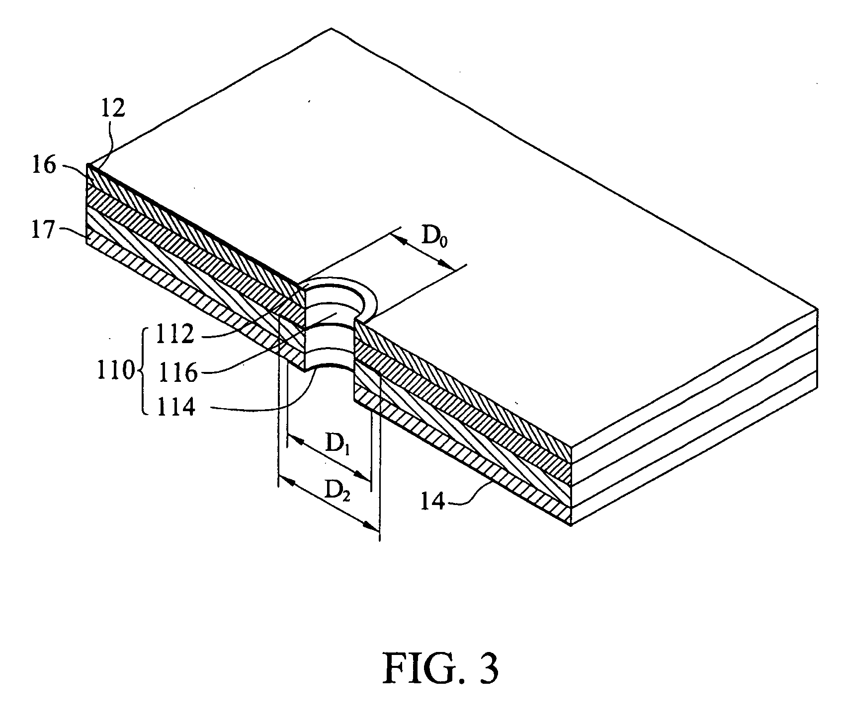
Coupled via structure, circuit board having the coupled via structure and method of manufacturing the circuit board
PatentActiveUS20200178386A1
Innovation
- A coupled via structure with facing plates that can adjust gap distance and width to match the characteristic impedance of coupled signal lines, comprising a plate via penetrating through the board body with a contact pad and connection line, allowing for precise control of impedance by varying the shape parameters.


Printed circuit board having vias
PatentInactiveUS20070000691A1
Innovation
- A via design with a smaller outer diameter for the pad connected to the input signal line and an unaltered or larger outer diameter for the pad connected to the output signal line, reducing the overall via capacitance and increasing impedance matching with the input signal line to minimize signal reflections.

Manufacturing Standards for High-Speed Via Design
Manufacturing standards for high-speed via design have evolved significantly to address the critical relationship between signal integrity and via structures in modern electronic systems. The establishment of comprehensive manufacturing guidelines ensures consistent production quality while maintaining the electrical performance characteristics essential for high-frequency applications.
Industry standards such as IPC-2221 and IPC-6012 provide fundamental frameworks for via manufacturing, specifying dimensional tolerances, aspect ratios, and plating requirements. These standards define critical parameters including via diameter consistency, typically maintaining tolerances within ±0.025mm for high-speed applications, and copper plating thickness uniformity to ensure reliable signal transmission paths.
Advanced manufacturing standards specifically address microvias and HDI (High Density Interconnect) structures, which are increasingly prevalent in high-speed designs. IPC-2315 establishes guidelines for microvia formation, including laser drilling parameters, aspect ratio limitations typically not exceeding 1:1 for reliability, and sequential lamination processes that maintain structural integrity while preserving electrical characteristics.
Quality control standards encompass comprehensive testing protocols including cross-sectional analysis, impedance verification, and time-domain reflectometry measurements. Manufacturing facilities must implement statistical process control methods to monitor via formation consistency, with acceptance criteria typically requiring 99.7% conformance to specified dimensional and electrical parameters.
Emerging standards address next-generation requirements such as glass-core substrates and advanced materials integration. These evolving guidelines incorporate new drilling technologies, alternative plating chemistries, and enhanced inspection methodologies using automated optical inspection and X-ray analysis to detect potential defects that could compromise signal integrity.
The integration of Design for Manufacturing (DFM) principles within these standards ensures that via structures can be reliably produced at scale while meeting increasingly stringent electrical performance requirements for applications operating at frequencies exceeding 25 GHz.
Cost-Performance Trade-offs in Via Structure Design
The cost-performance trade-offs in via structure design represent one of the most critical decision-making challenges in modern PCB development. Engineers must balance signal integrity requirements against manufacturing costs, production complexity, and design constraints. These trade-offs become increasingly complex as signal frequencies rise and board densities increase, forcing designers to make strategic compromises between optimal electrical performance and economic feasibility.
Manufacturing costs vary significantly across different via technologies. Through-hole vias remain the most cost-effective option for low-frequency applications, requiring standard drilling processes and conventional plating techniques. Blind and buried vias introduce substantial cost premiums due to sequential lamination processes and specialized drilling equipment, typically increasing manufacturing costs by 30-50%. Microvias, while offering superior electrical performance, can double or triple production costs due to laser drilling requirements and tighter process controls.
Performance benefits often justify higher costs in high-speed applications. Microvias provide reduced parasitic inductance and capacitance, enabling signal integrity improvements that can eliminate the need for expensive signal conditioning components. The shorter current return paths in microvia structures reduce electromagnetic interference, potentially allowing designers to use fewer ground planes and reduce overall board layer count, partially offsetting the increased via costs.
Design complexity introduces additional cost considerations beyond direct manufacturing expenses. Advanced via structures require sophisticated design tools, extended simulation cycles, and more experienced engineering resources. The increased design time and validation requirements can add 20-40% to development costs, particularly for first-time implementations of advanced via technologies.
Volume production economics significantly influence cost-performance decisions. High-volume consumer electronics can amortize advanced via costs across millions of units, making premium technologies economically viable. Conversely, low-volume industrial applications may require designers to accept performance compromises to maintain cost targets, leading to alternative solutions such as optimized routing strategies or component placement modifications.
Reliability considerations add another dimension to cost-performance analysis. While advanced via structures may increase initial costs, their improved reliability characteristics can reduce field failure rates and warranty expenses. The total cost of ownership calculation must include these long-term reliability benefits when evaluating via structure alternatives for mission-critical applications.
Unlock deeper insights with Patsnap Eureka Quick Research — get a full tech report to explore trends and direct your research. Try now!
Generate Your Research Report Instantly with AI Agent
Supercharge your innovation with Patsnap Eureka AI Agent Platform!