

Signal Integrity vs Noise Sources
MAR 26, 20269 MIN READ
Generate Your Research Report Instantly with AI Agent
PatSnap Eureka helps you evaluate technical feasibility & market potential.
Signal Integrity Background and Design Objectives
Signal integrity has emerged as one of the most critical challenges in modern electronic system design, fundamentally driven by the relentless pursuit of higher data rates, increased circuit density, and enhanced system performance. As digital systems continue to evolve toward multi-gigabit communication speeds and beyond, the preservation of signal quality throughout the transmission path has become paramount to ensuring reliable system operation.
The historical evolution of signal integrity concerns parallels the advancement of semiconductor technology and system complexity. In early digital systems operating at relatively low frequencies, signal integrity issues were often negligible or manageable through simple design practices. However, as clock frequencies increased from megahertz to gigahertz ranges and rise times decreased to picosecond levels, previously insignificant parasitic effects began to dominate system behavior, transforming signal integrity from a secondary consideration into a primary design constraint.
Contemporary electronic systems face unprecedented challenges in maintaining signal fidelity across increasingly complex interconnect networks. High-speed digital circuits, advanced packaging technologies, and dense printed circuit board layouts create environments where multiple noise sources can simultaneously degrade signal quality. These noise sources include crosstalk from adjacent signal lines, power delivery network fluctuations, electromagnetic interference, reflections from impedance discontinuities, and ground bounce phenomena.
The primary objective of signal integrity design is to ensure that digital signals maintain sufficient quality to enable reliable data transmission and system functionality. This encompasses maintaining appropriate signal amplitude levels, minimizing timing uncertainties, reducing noise coupling between circuits, and preserving signal edge quality throughout the transmission medium. Achieving these objectives requires comprehensive understanding of electromagnetic principles, transmission line theory, and noise coupling mechanisms.
Modern signal integrity design objectives extend beyond basic functionality to encompass system-level performance optimization. Engineers must balance competing requirements including power consumption, electromagnetic compatibility, manufacturing cost, and physical design constraints while maintaining robust signal quality. The integration of high-speed analog and digital circuits on common substrates further complicates these objectives, requiring sophisticated noise isolation and signal routing strategies.
The ultimate goal involves creating design methodologies and verification processes that can predict and mitigate signal integrity issues early in the development cycle, enabling first-pass design success while meeting increasingly stringent performance, cost, and time-to-market requirements in competitive technology markets.
Market Demand for High-Speed Signal Design Solutions
The global electronics industry is experiencing unprecedented demand for high-speed signal design solutions as digital transformation accelerates across multiple sectors. Modern electronic systems require increasingly sophisticated signal integrity management to handle higher data rates, reduced power consumption, and miniaturized form factors. This demand is particularly pronounced in telecommunications infrastructure, data centers, automotive electronics, and consumer devices where signal speeds continue to escalate.
Data center modernization represents one of the most significant growth drivers for high-speed signal design solutions. Cloud computing expansion and artificial intelligence workloads necessitate advanced interconnect technologies capable of managing multi-gigabit data transmission while minimizing electromagnetic interference. Server manufacturers and network equipment providers are actively seeking comprehensive signal integrity solutions that can address crosstalk, power delivery noise, and timing synchronization challenges simultaneously.
The automotive sector presents another substantial market opportunity as vehicles transition toward electric and autonomous systems. Advanced driver assistance systems, infotainment platforms, and electric vehicle power management systems require robust signal design solutions to ensure reliable operation in harsh electromagnetic environments. Automotive electronics manufacturers are increasingly prioritizing signal integrity tools that can handle both high-frequency digital signals and high-power switching noise sources.
Telecommunications infrastructure modernization, particularly the ongoing deployment of advanced wireless networks, continues to drive demand for sophisticated signal design capabilities. Network equipment manufacturers require solutions that can manage complex multi-layer circuit boards with mixed-signal environments, where high-speed digital processing coexists with sensitive analog radio frequency circuits.
Consumer electronics manufacturers face mounting pressure to deliver higher performance devices in increasingly compact packages. Mobile device designers, gaming console manufacturers, and wearable technology companies are seeking integrated signal integrity solutions that can address power delivery network optimization, electromagnetic compatibility, and thermal management within constrained design spaces.
The market demand extends beyond traditional hardware design to encompass comprehensive simulation and analysis tools. Engineering teams require advanced modeling capabilities that can predict signal behavior, identify potential noise sources, and optimize circuit performance before physical prototyping. This trend reflects the industry's shift toward simulation-driven design methodologies to reduce development costs and accelerate time-to-market.
Current SI Challenges and Noise Source Limitations
Signal integrity challenges in modern electronic systems have intensified dramatically as operating frequencies continue to escalate and device geometries shrink. High-speed digital circuits operating at multi-gigahertz frequencies face severe timing uncertainties, with jitter accumulation becoming a critical bottleneck. Advanced packaging technologies, including 2.5D and 3D integration, introduce complex electromagnetic coupling effects that traditional design methodologies struggle to predict and mitigate.
Power delivery networks represent another significant challenge area, where simultaneous switching noise (SSN) can cause voltage fluctuations exceeding acceptable thresholds. The increasing current demands of modern processors, combined with tighter voltage margins, create scenarios where even minor power supply variations can trigger logic errors or performance degradation.
Crosstalk between adjacent signal traces has evolved beyond simple capacitive and inductive coupling. In high-density interconnect environments, far-end crosstalk can approach signal amplitudes comparable to the intended signal, particularly in differential pair configurations where skew mismatches exacerbate the problem. Multi-aggressor scenarios, where multiple switching signals simultaneously affect a victim trace, present analysis complexities that exceed traditional worst-case modeling approaches.
Electromagnetic interference sources have proliferated with the integration of mixed-signal components on single substrates. Switching power supplies, clock distribution networks, and high-frequency digital circuits generate broadband noise spectra that can couple through substrate, package, and board-level pathways. The challenge intensifies in automotive and industrial applications where external electromagnetic environments add unpredictable interference sources.
Return path discontinuities in multilayer printed circuit boards create current loops that generate both radiated emissions and susceptibility issues. Via transitions between layer pairs, particularly in high-speed differential signaling, introduce impedance discontinuities that manifest as reflection-induced noise. These effects become more pronounced as signal rise times decrease below 100 picoseconds.
Thermal noise limitations in sensitive analog circuits, combined with increased digital switching activity, create signal-to-noise ratio challenges that impact overall system performance. The proximity of high-power digital processing units to sensitive RF front-ends compounds these issues, requiring sophisticated isolation and filtering strategies that often conflict with miniaturization objectives.
Existing Noise Mitigation and SI Enhancement Solutions
01 Signal integrity analysis and testing methods
Various methods and systems are employed to analyze and test signal integrity in electronic circuits and systems. These approaches include measurement techniques, simulation tools, and testing equipment designed to evaluate signal quality, detect distortions, and identify potential issues in signal transmission. Advanced analysis methods help engineers assess signal degradation, timing issues, and electromagnetic interference effects on signal paths.- Signal integrity analysis and testing methods: Various methods and systems are employed to analyze and test signal integrity in electronic circuits and systems. These approaches include measurement techniques, simulation tools, and testing methodologies to evaluate signal quality, identify potential issues, and ensure proper signal transmission. The methods encompass both time-domain and frequency-domain analysis to characterize signal behavior and detect anomalies such as reflections, crosstalk, and noise.
- Impedance matching and transmission line design: Proper impedance matching and transmission line design are critical for maintaining signal integrity in high-speed circuits. Techniques include optimizing trace geometry, implementing controlled impedance structures, and designing termination schemes to minimize signal reflections and distortions. These approaches ensure that signals propagate efficiently through interconnects without degradation, particularly important in printed circuit boards and high-frequency applications.
- Crosstalk reduction and electromagnetic interference mitigation: Methods for reducing crosstalk and electromagnetic interference are essential for preserving signal integrity in densely packed electronic systems. Techniques include physical separation of signal traces, implementation of shielding structures, use of differential signaling, and optimization of ground plane configurations. These approaches minimize unwanted coupling between adjacent signals and reduce susceptibility to external electromagnetic disturbances.
- Equalization and signal conditioning techniques: Equalization and signal conditioning techniques are employed to compensate for signal degradation in high-speed data transmission. These methods include pre-emphasis, de-emphasis, continuous-time linear equalization, and decision feedback equalization to restore signal quality after transmission through lossy channels. Such techniques are particularly important in modern communication systems where data rates continue to increase and signal integrity challenges become more pronounced.
- Power integrity and supply noise management: Power integrity management is closely related to signal integrity, focusing on maintaining stable power delivery and minimizing supply noise that can affect signal quality. Techniques include decoupling capacitor placement, power distribution network optimization, and simultaneous switching noise reduction. Proper power integrity design ensures that voltage fluctuations and ground bounce do not compromise signal integrity in high-performance electronic systems.
02 Signal integrity improvement through circuit design optimization
Circuit design techniques are utilized to enhance signal integrity by optimizing trace routing, impedance matching, and component placement. These design methodologies focus on minimizing signal reflections, crosstalk, and electromagnetic interference. Design considerations include proper termination schemes, controlled impedance structures, and strategic placement of decoupling capacitors to maintain signal quality throughout the transmission path.Expand Specific Solutions03 High-speed signal transmission and interconnect technologies
Technologies and structures for high-speed signal transmission address challenges in maintaining signal integrity at elevated data rates. These solutions encompass advanced interconnect designs, differential signaling techniques, and specialized transmission line structures. Implementation strategies focus on reducing signal loss, managing timing skew, and ensuring reliable data transmission in high-frequency applications.Expand Specific Solutions04 Signal integrity monitoring and compensation systems
Monitoring and compensation systems are implemented to maintain signal integrity in real-time operations. These systems include adaptive equalization circuits, signal conditioning mechanisms, and feedback control loops that dynamically adjust signal parameters. The technologies enable continuous monitoring of signal quality and automatic correction of degradation effects to ensure reliable data transmission.Expand Specific Solutions05 Signal integrity in packaging and board-level integration
Packaging and board-level integration techniques address signal integrity challenges in multi-layer structures and complex assemblies. These approaches include advanced substrate materials, via design optimization, and power distribution network design. Solutions focus on minimizing parasitic effects, reducing ground bounce, and maintaining signal quality across different packaging levels and interconnection interfaces.Expand Specific Solutions
Key Players in SI Analysis and EDA Tool Industry
The signal integrity versus noise sources technology landscape represents a mature yet rapidly evolving market driven by increasing demand for high-speed digital communications and advanced semiconductor applications. Major semiconductor leaders including Intel, Texas Instruments, QUALCOMM, and NVIDIA dominate the competitive landscape through comprehensive signal integrity solutions spanning processors, analog circuits, and specialized chipsets. The technology has reached commercial maturity with established players like Agilent Technologies and Rambus providing sophisticated measurement tools and interface architectures. Emerging applications in 5G, automotive electronics, and AI accelerators are driving continued innovation, with companies like MediaTek, NXP, and Broadcom (Avago) developing next-generation solutions. The market demonstrates strong consolidation among tier-one suppliers while maintaining robust growth potential across telecommunications, consumer electronics, and industrial segments.
Texas Instruments Incorporated
Technical Solution: TI provides comprehensive signal integrity solutions through their high-performance analog and mixed-signal portfolio. Their approach focuses on low-noise amplifiers, precision voltage references, and advanced power management ICs that minimize electromagnetic interference. TI's signal conditioning products feature integrated shielding techniques and differential signaling architectures to combat common noise sources including power supply ripple, crosstalk, and ground bounce. Their ISO7741 digital isolators achieve >100dB common-mode transient immunity while maintaining signal fidelity across isolation barriers.
Strengths: Extensive analog expertise, proven low-noise designs, comprehensive product portfolio. Weaknesses: Higher cost compared to discrete solutions, limited customization for specialized applications.
Intel Corp.
Technical Solution: Intel addresses signal integrity challenges through advanced packaging technologies and on-die noise mitigation techniques. Their approach includes embedded decoupling capacitors, power delivery network optimization, and simultaneous switching noise reduction through controlled impedance design. Intel's processors incorporate dedicated power islands and clock gating to minimize switching noise impact on sensitive analog circuits. Their chipset designs feature advanced EMI shielding and ground plane optimization to maintain signal quality in high-speed digital environments with frequencies exceeding 5GHz.
Strengths: Leading-edge process technology, integrated system-level solutions, extensive R&D resources. Weaknesses: Focus primarily on digital applications, limited standalone analog signal integrity products.
Core Innovations in SI Modeling and Noise Control
DFE implementation for wireline applications
PatentPendingUS20240121139A1
Innovation
- The implementation of a decision feedback equalizer (DFE) that estimates and subtracts inter-symbol-interference from received signals using a least mean squares (LMS) error algorithm, combined with parallel and pseudo-static dynamic architectures to reduce computational complexity and meet high data throughput requirements.


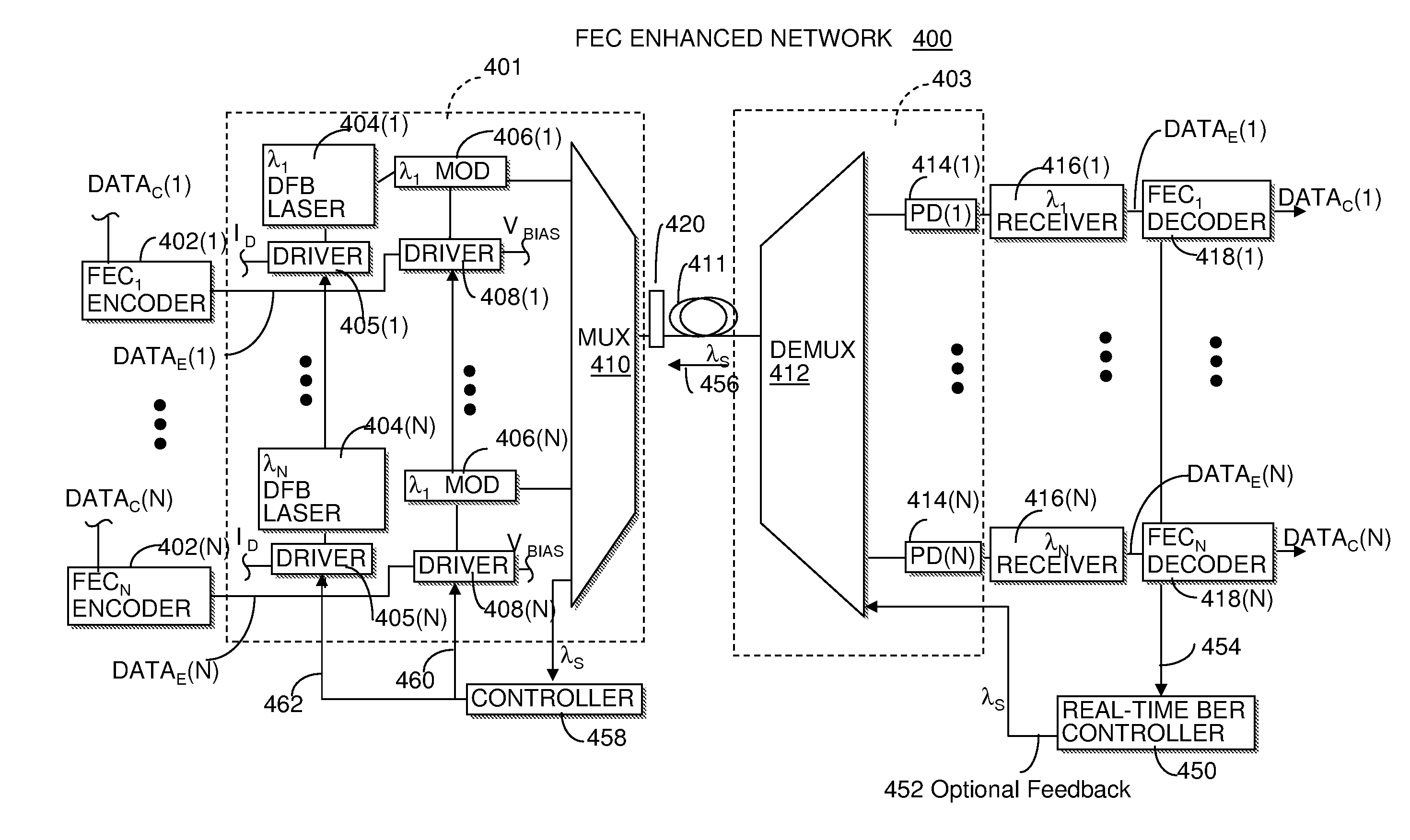
Forward error correction (FEC) enabled photonic integrated circuit (PICs) chips with multiple signal channels
PatentInactiveUS7734191B1
Innovation
- The implementation of forward error correction (FEC) in combination with multi-channel PICs, which allows for relaxed operating parameter specifications, wider design choices in channel count and spacing, and compensation for transmission penalties such as relative intensity noise and dispersion penalties, enabling the transmission of distorted channel signals with FEC encoding to improve BER performance.

EMC Compliance Standards for Signal Integrity
Electromagnetic Compatibility (EMC) compliance standards serve as the fundamental framework for ensuring signal integrity in electronic systems by establishing mandatory requirements for electromagnetic emissions and immunity. These standards define acceptable limits for conducted and radiated emissions while specifying minimum immunity levels that electronic devices must withstand when exposed to electromagnetic disturbances.
The International Electrotechnical Commission (IEC) and Federal Communications Commission (FCC) represent the primary regulatory bodies establishing global EMC standards. IEC 61000 series standards provide comprehensive guidelines for electromagnetic compatibility, with specific focus on signal integrity requirements for different product categories. FCC Part 15 regulations govern electromagnetic emissions for digital devices in the United States, establishing strict limits on unintentional radiators that could interfere with licensed radio services.
CISPR (International Special Committee on Radio Interference) standards complement IEC requirements by addressing specific emission limits for information technology equipment and multimedia devices. CISPR 32 establishes emission requirements for multimedia equipment, while CISPR 35 defines immunity requirements, both directly impacting signal integrity design considerations. These standards mandate specific measurement procedures and limit values that electronic systems must meet to ensure minimal electromagnetic interference.
Military and aerospace applications require adherence to more stringent standards such as MIL-STD-461, which establishes electromagnetic interference and compatibility requirements for defense systems. This standard addresses both conducted and radiated emissions with significantly lower limit values compared to commercial standards, reflecting the critical nature of signal integrity in defense applications.
Automotive EMC standards, particularly ISO 11452 and CISPR 25, address the unique electromagnetic environment within vehicles where multiple electronic systems operate in close proximity. These standards establish specific test methods for bulk current injection, radiated immunity, and conducted transients that directly affect automotive signal integrity performance.
Compliance verification requires systematic testing using standardized measurement procedures, calibrated equipment, and accredited test facilities. Pre-compliance testing during design phases enables early identification of signal integrity issues, while final compliance testing validates that production units meet all applicable EMC requirements before market introduction.
AI-Driven SI Optimization and Predictive Analysis
The integration of artificial intelligence into signal integrity optimization represents a paradigm shift from traditional reactive design approaches to proactive, predictive methodologies. Machine learning algorithms are increasingly being deployed to analyze complex electromagnetic interactions and predict signal degradation patterns before physical prototyping stages. These AI-driven systems leverage vast datasets of simulation results, measurement data, and design parameters to establish correlations between design choices and signal integrity outcomes.
Deep learning neural networks have demonstrated remarkable capability in identifying subtle patterns within high-frequency signal behavior that conventional analysis methods often overlook. Convolutional neural networks excel at processing S-parameter data and eye diagram patterns, while recurrent neural networks prove effective in analyzing time-domain signal characteristics. These models can predict crosstalk levels, impedance discontinuities, and timing violations with accuracy rates exceeding 95% in controlled environments.
Predictive analysis frameworks now incorporate real-time design rule checking, automatically flagging potential signal integrity violations during the layout phase. Advanced algorithms analyze trace routing, via placement, and component positioning to forecast signal quality metrics before electromagnetic simulation. This proactive approach significantly reduces design iteration cycles and accelerates time-to-market for high-speed digital products.
Reinforcement learning techniques are emerging as powerful tools for automated PCB optimization, where AI agents learn optimal routing strategies through iterative design exploration. These systems can simultaneously optimize multiple objectives including signal integrity, electromagnetic compatibility, and thermal management. The agents develop sophisticated understanding of design trade-offs, often discovering non-intuitive solutions that human designers might overlook.
Cloud-based AI platforms are democratizing access to advanced signal integrity optimization tools, enabling smaller design teams to leverage enterprise-level predictive capabilities. These platforms continuously learn from global design databases, improving prediction accuracy and expanding their knowledge base across diverse application domains and technology nodes.
Unlock deeper insights with PatSnap Eureka Quick Research — get a full tech report to explore trends and direct your research. Try now!
Generate Your Research Report Instantly with AI Agent
Supercharge your innovation with PatSnap Eureka AI Agent Platform!